EP2953216B1 - Éclateur doté d'un dispositif d'amortissement et/ou de refroidissement - Google Patents
Éclateur doté d'un dispositif d'amortissement et/ou de refroidissement Download PDFInfo
- Publication number
- EP2953216B1 EP2953216B1 EP15170367.5A EP15170367A EP2953216B1 EP 2953216 B1 EP2953216 B1 EP 2953216B1 EP 15170367 A EP15170367 A EP 15170367A EP 2953216 B1 EP2953216 B1 EP 2953216B1
- Authority
- EP
- European Patent Office
- Prior art keywords
- spark gap
- electrode
- discs
- auxiliary ignition
- spark
- Prior art date
- Legal status (The legal status is an assumption and is not a legal conclusion. Google has not performed a legal analysis and makes no representation as to the accuracy of the status listed.)
- Active
Links
Images


Classifications
-
- H—ELECTRICITY
- H01—ELECTRIC ELEMENTS
- H01T—SPARK GAPS; OVERVOLTAGE ARRESTERS USING SPARK GAPS; SPARKING PLUGS; CORONA DEVICES; GENERATING IONS TO BE INTRODUCED INTO NON-ENCLOSED GASES
- H01T2/00—Spark gaps comprising auxiliary triggering means
- H01T2/02—Spark gaps comprising auxiliary triggering means comprising a trigger electrode or an auxiliary spark gap
-
- H—ELECTRICITY
- H01—ELECTRIC ELEMENTS
- H01T—SPARK GAPS; OVERVOLTAGE ARRESTERS USING SPARK GAPS; SPARKING PLUGS; CORONA DEVICES; GENERATING IONS TO BE INTRODUCED INTO NON-ENCLOSED GASES
- H01T1/00—Details of spark gaps
- H01T1/02—Means for extinguishing arc
-
- H—ELECTRICITY
- H01—ELECTRIC ELEMENTS
- H01T—SPARK GAPS; OVERVOLTAGE ARRESTERS USING SPARK GAPS; SPARKING PLUGS; CORONA DEVICES; GENERATING IONS TO BE INTRODUCED INTO NON-ENCLOSED GASES
- H01T1/00—Details of spark gaps
- H01T1/02—Means for extinguishing arc
- H01T1/08—Means for extinguishing arc using flow of arc-extinguishing fluid
- H01T1/10—Means for extinguishing arc using flow of arc-extinguishing fluid with extinguishing fluid evolved from solid material by heat of arc
-
- H—ELECTRICITY
- H01—ELECTRIC ELEMENTS
- H01T—SPARK GAPS; OVERVOLTAGE ARRESTERS USING SPARK GAPS; SPARKING PLUGS; CORONA DEVICES; GENERATING IONS TO BE INTRODUCED INTO NON-ENCLOSED GASES
- H01T1/00—Details of spark gaps
- H01T1/15—Details of spark gaps for protection against excessive pressure
-
- H—ELECTRICITY
- H01—ELECTRIC ELEMENTS
- H01T—SPARK GAPS; OVERVOLTAGE ARRESTERS USING SPARK GAPS; SPARKING PLUGS; CORONA DEVICES; GENERATING IONS TO BE INTRODUCED INTO NON-ENCLOSED GASES
- H01T4/00—Overvoltage arresters using spark gaps
- H01T4/16—Overvoltage arresters using spark gaps having a plurality of gaps arranged in series
Definitions
- the invention relates to a spark gap with cooling and / or damping device.
- spark gaps Numerous arrangements for spark gaps are known in the prior art. It should be noted that spark gaps are not trivial arrangements, but for a reliable ignition and for the cooling of the resulting plasma arc a not to be underestimated effort must be driven. Previous spark gaps were characterized by a specific to be taken pulse energy.
- EP 1 542 323 A2 shows a spark gap with a starting aid with a voltage-switching element.
- FIGS. 1 and 2 show a first arrangement according to embodiments of the invention in two different states.
- the spark gap 1 an adaptive cooling and / or damping device, which will be explained in more detail below.
- the spark gap 1 has at least a first spark gap electrode FS 1 and a second spark gap electrode FS 2.
- the spark gap can also have further electrodes for different purposes.
- measuring electrodes may be provided to measure, for example, the degradation of insulating components within the spark gap in a capacitive, inductive or resistive manner.
- the spark gap 1 has at least one auxiliary ignition electrode ZE for connection to an ignition circuit.
- auxiliary ignition electrode ZE is spatially adjacent to the first spark gap electrode FS 1 and spaced from the second spark gap electrode FS 2 .
- Ignition auxiliary electrode ZE based on the direction of the first spark gap electrode FS 1 and second spark gap electrode FS 2 arranged laterally to this direction.
- a low-conductivity material BRZ is introduced for ignition assistance. That is, in the event of an overvoltage, ionization will first take place via the auxiliary starting electrode and the first spark gap electrode FS 1 , and then the main spark gap between the first spark gap electrode FS 1 and the second spark gap electrode FS 2 will be ignited.
- a plurality of slices S 1 , S 2 ,... S n are now introduced between the auxiliary starting electrode ZE and the second spark gap electrode FS 2 .
- These plurality of disks S 1 , S 2 ,... S n are electrically insulated from the auxiliary starting electrode ZE and the first spark gap electrode FS 1 by means of an electrical insulator ISO 1 .
- the slices S 1 , S 2 , ... S n each have an opening, wherein the openings of the slices S 1 , S 2 , ... S n are arranged so that they form an arc channel between the second spark gap electrode FS second and the first spark gap electrode FS 1 .
- These plurality of disks S 1 , S 2 , ... S n serve as cooling and / or damping device.
- FIG. 1 In the case of FIG. 1 is the spark gap in the off state, ie the spark gap 1 does not conduct electricity. If there is now a current flow, ie the spark gap ignites, then an arc plasma is formed.
- the spark gap 1 can now adjust to the event.
- the arc plasma will build up a correspondingly higher heat and pressure, so that now through the pressure effect the disks in the lateral direction as in FIG. 2 shown can be pushed apart. This extends on the one hand the spark gap channel, because at the same time.
- the arc plasma and the resulting heat to the environment can be derived according to the arrows in the interstices of the discs. Since now at least a portion of the ionized gas is removed from the spark gap channel, the conductivity of the arc plasma decreases. Since energy is needed to move the disks and at least a portion of the pressure escapes when the disks are pushed apart, the pressure increase is damped.
- the spark gap electrodes may be made of WCu or other preferably arc-resistant materials.
- discs S 1 , S 2 , ... S n are made of a suitable material.
- the slices S 1 , S 2 ,... S n from a hard-gasifying material such as polyoxymethylene (POM) or from polyetheretherketone (PEEK), the slices S 1 , S 2 , n preferably made of an arc-resistant material such as WCu (tungsten-copper), so that usually a variety of pulse events can be derived.
- a hard-gasifying material such as polyoxymethylene (POM) or from polyetheretherketone (PEEK)
- PEEK polyetheretherketone
- At least part of the plurality of slices S 1 , S 2 ,... S n may comprise an electrically conductive material.
- the heat capacity for the Selection should be a criterion.
- the disks may comprise copper or tungsten or compounds thereof.
- At least a portion of the plurality of slices S 1 , S 2 ,... S n may comprise an electrically nonconductive material.
- heat capacity for the selection can be a criterion.
- the discs may have ceramic.
- the plurality of electrically conductive panes S 1 , S 2 ,... S n can have a more or less temperature-resistant material.
- At least a portion of the plurality of slices S 1, S 2, ... S n grooves or electrically conductive / non-conductive spacers have R as shown in FIG. 4 shown.
- one or more of the (electrically conductive or electrically insulating) disks S 1 , S 2 ,... S n have a porous material.
- a porous or sintered material may be used.
- An essential aspect of a porous material is that this material forms channels, so that a plasma of the spark gap can be derived attenuated.
- porous material may include (sintered) sand (resulting in a solid shape), and / or spheres made of, for example, steel, POM, ceramic and / or flux or fibers, for example of ceramic material.
- Both the grooves and the spacers as well as the grooves R allow plasma to escape directly at the beginning of an impulse event. If a stronger pulse event occurs, then the slices S 1 , S 2 ,... S n can be pushed apart in order to further assist the outflow under the influence of the further increasing pressure. However, this is not absolutely necessary.
- the spacers or grooves R in the individual panes can be introduced into the surface, for example, by stamping, pressing or embossing. If several discs are stacked, depending on the position of the spacers or grooves to each other a free volume between the discs are generated. The plasma has the possibility to flow outward through this free volume. The same applies to spacers which can be applied to the surface of the slices S 1 , S 2 ,... S n alternatively or additionally.
- a hard gas insulating material is not mandatory for insulation ISO 1 adjacent to the first spark gap electrode FS 1 , it is advantageous for effective cooling of the arc plasma because hard gas materials have the property of narrowing the arc channel.
- the low-conductive material BRZ and / or the auxiliary ignition electrode ZE may have an annular opening, wherein the openings of the slices S 1 , S 2 , ... S n are arranged so that they form an arc channel between the second spark gap electrode FS 2 and the form the first spark gap electrode FS 1 .
- the spark gap channel can now also be designed in the connecting direction from the first spark gap electrode to the second spark gap electrode.
- a cylindrical channel for example, a slightly eccentric opening arranged as in Fig. 3
- On the right side shown in the discs cause that at a certain angular displacement of the discs to each other results in a helical path.
- a slot-like opening as in FIG. 3 can be reached on the left side.
- the openings can in principle take all possible forms. It is also possible to use a part of the disks in one mold and another part in another mold.
- the individual elements are held only by their own weight, in which case it is expedient to provide guide devices so that the individual elements return to their previous position after being pushed apart.
- the adaptive property can only be used once, e.g. in that the elements are suitably pressure-releasably connected.
- the elements are suitably pressure-releasably connected.
- a suitable adhesive or a solder e.g.
- the spark gap 1 has an elastic element D, so that the spark gap electrodes FS 1 , FS 2 and the slices S 1 , S 2 , ... S n are held.
- an elastic element D may be a pressurization by means of a spring or a circumferential elastic element, for example, of an elastomer similar to a rubber band or the like.
- the spark gap 1 may also have a encompassing housing G.
- the housing G can also combine the function of the elastic element.
- an outflow is now either possible only in the intermediate regions of the disks or, as far as the housing G has openings, plasma can continue to escape into the environment.
- arc diaphragm ISO 2 In order to direct the arc plasma targeted can also be provided that between the slices S 1 , S 2 , ... S n and the auxiliary ignition electrode ZE an arc diaphragm ISO 2 is attached.
- the spark gap has an elastic element D, so that the spark gap electrodes FS 1 , FS 2 and the disks S 1 , S 2 , ... S n (pressure-displaceable) are held and that the electrically conductive disks S 1 , S 2 , ... S n can be displaced in the direction of the first spark gap electrode and the second spark gap electrode.
- the spark gap according to the invention can also be used in a spark gap arrangement with an ignition circuit, the ignition circuit connecting the second spark gap electrode FS 2 and the auxiliary ignition electrode ZE via a voltage-switching and / or voltage-limiting element.
- the ignition circuit connecting the second spark gap electrode FS 2 and the auxiliary ignition electrode ZE via a voltage-switching and / or voltage-limiting element.
- this can be done as in FIG. 1 and 2 a varistor and a gas discharge tube may be provided.
- the second spark gap electrode FS 2 is contacted with the auxiliary ignition electrode ZE by a voltage-switching element and / or a voltage-limiting element (for example a varistor), whereby a continuous current flow through the ignition circuit can be prevented.
- a voltage-switching element and / or a voltage-limiting element for example a varistor
- the upper potential is conducted to the auxiliary starting electrode ZE via the voltage-switching and / or the voltage-limiting element.
- the low-conductivity material BRZ At least part of the surface burns to the first spark gap electrode FS 1 and ionizes the combustion channel.
- the plasma creates a main discharge between the two spark gap electrodes.
- Insulation material ISO 1 or ISO 2 gasifies and cools the arc.
- the temperature and the pressure increase. From a certain threshold value of the pressure, the disks S 1 , S 2 , ... S n are pressed apart and thus form several large blow-off volumes, through which the ionized gas can escape.
- the plasma can be strongly cooled by the large surfaces between the discs.
- the structure thus forms a self-regulating system, since the pressure build-up and the pressure reduction depend on each other and simultaneously counteract each other.
- the distance between the discs is dimensioned so that the flow of the plasma is inhibited so much that outside the arrangement no or only very small amounts of ionized gas escape.
- the spacing of the cooling surfaces can be achieved by insulating or non-insulating and resistive, as well as a combination of insulating as non-insulating and resistive spacers.
- the invention makes it possible to adjust the outflow area adaptively to different requirements by means of different pulse energies.
- the arrangement according to the invention is simple to realize mechanically.
- the invention allows to provide a high discharge capacity by a large thermal mass.
- the high thermal mass also has a large surface, resulting in a high energy absorption.
- the plasma channel can be deionized and thus the conductivity of the plasma can be reduced.
- Other cooling mechanisms can be used to achieve efficient cooling and removal of the plasma.
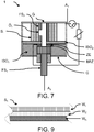
- FIG. 5 is another illustrative embodiment, which is not part of the invention shown. This differs initially only in the shape of the disc S. 1
- the disc of FIG. 5 and FIG. 6 is not a disk of solid material but rather resembles (in plan view) a snail.
- Suitable screws - indicated in FIG. 6 - Can be made of sheet-metal material wound (particularly simple and inexpensive production) or milled from solid material or produced as such, for example by casting-like process.
- the properties of the winding ie the number of windings and the geometry of the channel created thereby, the properties such as flow behavior and cooling behavior can be specifically influenced.
- the material may be insulating or electrically conductive.
- a channel through the plasma of an arc can escape steamed. If the screw is constructed of a suitable material, then this can be used in addition to the cooling. In this case, the channel may be both uniform and irregular, such as in FIG. 6 indicated.
- the walls of the screw S 1 can run parallel to each other over the entire length, converge toward one another or diverge.
- the material in a worm shape S 1 may consist of one or more layers and different materials.
- material in a worm shape S 1 may comprise a conductive material such as copper or non-conductive material such as ceramic (as a flux or as a solid material).
- a layer structure may be comprised of one or more layers of ceramic and / or metal adjacent to an outgassing material, such as e.g. Polyoxymethylene (POM) be constructed.
- an outgassing material such as e.g. Polyoxymethylene (POM) be constructed.
- openings may also be provided in the other layers, which are either given by the material property itself and / or are particularly provided. Is e.g. the outgassing material is arranged in a (coarse) porous ceramic or in a wire-like grid is given a good access to the outgassing material with simultaneous stability.
- the number of openings can be distributed differently, so that, for example, in order to realize a smaller material removal in the multilayer material in a screw shape S 1 , the openings can be selectively attached, for example to minimize outgassing close to the spark gap.
- the number of holes (voids) increases with respect to the length of the channel.
- the (electrically conductive) material in a screw shape S 1 forms an opening, wherein the openings are arranged so that it forms an arc channel between the second spark gap electrode FS 2 and the first spark gap electrode FS 1 .
- the (electrically conductive) material S 1 can also be embodied as part of the second spark gap electrode FS 2 .
- the material S 1 is usually made in one piece and electrically conductive with the spark gap electrode FS 2 .
- the (electrically conductive) material S 1 is a separate component, then it may, if necessary, also be configured in such a way that, under the pressure of a plasma, an expansion of the channel formed can also take place. Ie similar to the Embodiment before, the spiral configuration can change their properties depending on the pressure.
- the housing G may have areas in which plasma could also escape to the outside. These areas are shown, for example, as a dotted housing G.
- FIG. 5 only a single disc S 1 is shown, it is obvious to the person skilled in the art that a plurality of discs can also be mounted one above the other in a corresponding arrangement. In this case, mixed forms can also be used. For example, individual discs can be used accordingly FIG. 6 be executed while other discs according to Figures 3 or 4 are executed.
- FIG. 5 may be provided that in the material in a worm shape S 1 further openings ⁇ 1 are provided so that plasma of the ignited spark gap can enter at more than one point in the channel.
- the second spark gap electrode FS 2 has at least one further opening ⁇ 1 , so that plasma can enter laterally into the channel formed by the material in a screw shape S 1 .
- FIG. 8 A possible sectional view through the second spark gap electrode FS and the material in a screw shape S 1 is shown in FIG FIG. 8 shown.
- the present invention provides a large thermal mass and surface in which the plasma has the opportunity to cool.
- the spiral shape and the imperfections to the partition wall dampening the plasma flow, resulting in a reduction of the thermal energy.
- a back pressure is generated, so that during the high-current phase, the conductivity in the combustion chamber is increased and the energy conversion in the spark gap decreases.
- the back pressure and the conductivity in the spark gap decrease.
- a higher arc burn voltage is produced, resulting in improved line follow current extinguishing capability.
- the material described above in a worm shape S 1 may comprise a conductive material and / or a non-conductive material.
- an inner wall W I and an outer wall W A can be made of a rather massive material with holes or a net-like material, which together include a porous material W Z located therebetween.
- porous material may include (sintered) sand (resulting in a solid shape), and / or spheres made of, for example, steel, POM, ceramic and / or flux or fibers, for example of ceramic material.
- low-conductivity material BRZ it may be any suitable material.
- the low conductivity material BRZ may be made of, for example, FR4, a material used for printed circuit boards consisting of an epoxy resin-filled glass fiber fabric, with a suitable surface coating such as graphite.
- any material made of plastic or ceramic is suitable, which has a certain conductivity, be it that the respective material corresponding conductive materials such as electrically conductive ceramics or graphite (embedded) or coated with these is.
Landscapes
- Plasma Technology (AREA)
Claims (13)
- Eclateur (1) comportant un dispositif de refroidissement et/ou d'amortissement, présentant• au moins une première électrode d'éclateur (FS1) et une seconde électrode d'éclateur (FS2),• au moins une électrode d'allumage auxiliaire (ZE) pour relier avec un circuit d'allumage, dans lequel l'électrode d'allumage auxiliaire (ZE) est disposée en étant voisine spatialement de la première électrode d'éclateur (FS1) et espacée de la deuxième électrode d'éclateur (FS2), dans lequel l'électrode d'allumage auxiliaire (ZE), par rapport à la direction de la première électrode d'éclateur et de la deuxième électrode d'éclateur est disposée latéralement à celles-ci,• dans lequel entre l'électrode d'allumage auxiliaire (ZE) et la deuxième électrode d'éclateur (FS2) une pluralité de plaquette (S1,S2,...,Sn) isolées (ISO1) par rapport à l'électrode d'allumage auxiliaire (ZE) et la première électrode d'éclateur (FS1) sont montées,caractérisé en ce que les plaquettes (S1, S2,...,Sn) présentent des ouvertures, dans lequel les ouvertures des plaquettes sont disposées de telle sorte qu'elles forment un canal d'arc électrique entre la deuxième électrode d'éclateur (FS2) et la première électrode d'éclateur (FS1) et en ce que entre l'électrode d'allumage auxiliaire (ZE) et la première électrode d'éclateur (FS1) un matériau le moins conducteur possible (BRZ) pour l'assistance à l'allumage est inséré et en ce que la pluralité de plaquettes (S1, S2,...,Sn) peuvent être coulissées en s'écartant les unes des autres sous l'effet de la pression.
- Eclateur selon la revendication 1, caractérisé en ce que au moins une partie de la pluralité de plaquettes (S1, S2, ..., Sn) présentent des stries ou des écarteurs électriquement conducteurs/non conducteurs, qui servent d'écarteurs.
- Eclateur selon une des revendications précédentes, caractérisé en ce que l'éclateur présente un élément élastique (D) de sorte que les électrodes d'éclateur (FS1, FS2) et les plaquettes (S1, S2, ..., Sn) soient maintenues.
- Eclateur selon une des revendications précédentes, caractérisé en ce que au moins une de la pluralité de plaquettes (S1, S2, ..., Sn) présente un matériau conducteur et/ou un matériau non conducteur.
- Eclateur selon une des revendications précédentes, caractérisé en ce que l'isolation (ISO1) présente un matériau résistant aux gaz à proximité de la première électrode d'éclateur (FS1).
- Eclateur selon une des revendications précédentes, caractérisé en ce que au moins une pluralité de plaquettes (S1, S2, ..., Sn) présentent un matériau résistant à un arc électrique.
- Eclateur selon une des revendications précédentes, caractérisé en ce que le matériau le moins conducteur possible (BRZ) et/ou l'électrode d'allumage auxiliaire (ZE) présentent une ouverture annulaire, dans lequel les ouvertures sont disposées dans les plaquettes (S1, S2, ..., Sn) de telle sorte qu'elles forment un canal d'arc électrique entre la deuxième électrode d'éclateur (FS2) et la première électrode d'éclateur (FS1).
- Eclateur selon une des revendications précédentes, caractérisé en ce que au moins une de la pluralité de plaquettes (S1, S2, ... Sn) présente un matériau résistant aux températures.
- Eclateur selon une des revendications précédentes, caractérisé en ce que le canal d'arc électrique présente un façonnage cylindrique ou hélicoïdal en forme d'alésage oblong ou elliptique.
- Eclateur selon une des revendications précédentes, caractérisé en ce que les capteurs présente un élément élastique (D), de sorte que les électrodes d'éclateur (FS1, FS2) et/ou les plaquettes (S1, S2, ..., Sn) soient maintenues.
- Eclateur selon une des revendications précédentes, caractérisé en ce que entre une de la pluralité de plaquettes (S1, S2, ..., Sn) et l'électrode d'allumage auxiliaire (ZE) un écran d'arc électrique (ISO2) est monté.
- Dispositif d'éclateur comportant un éclateur selon une des revendications précédentes, caractérisé en ce que un circuit d'allumage est en outre fourni, qui relie la deuxième électrode d'éclateur (FS2) et l'électrode d'allumage auxiliaire (ZE) par l'intermédiaire d'un élément commutateur de tension et/ou un élément limitateur de tension.
- Eclateur selon une des revendications précédentes, caractérisé en ce que l'éclateur présente un boîtier enveloppant (G).
Priority Applications (1)
| Application Number | Priority Date | Filing Date | Title |
|---|---|---|---|
| EP16186267.7A EP3118951B1 (fr) | 2014-06-03 | 2015-06-03 | Éclateur dote d'un dispositif d'amortissement et/ou de refroidissement |
Applications Claiming Priority (2)
| Application Number | Priority Date | Filing Date | Title |
|---|---|---|---|
| DE102014210516.1A DE102014210516C5 (de) | 2014-06-03 | 2014-06-03 | Funkenstrecke |
| DE202015100397.8U DE202015100397U1 (de) | 2015-01-28 | 2015-01-28 | Funkenstrecke mit adaptiver Kühl- und/oder Dämpfungseinrichtung |
Related Child Applications (2)
| Application Number | Title | Priority Date | Filing Date |
|---|---|---|---|
| EP16186267.7A Division-Into EP3118951B1 (fr) | 2014-06-03 | 2015-06-03 | Éclateur dote d'un dispositif d'amortissement et/ou de refroidissement |
| EP16186267.7A Division EP3118951B1 (fr) | 2014-06-03 | 2015-06-03 | Éclateur dote d'un dispositif d'amortissement et/ou de refroidissement |
Publications (3)
| Publication Number | Publication Date |
|---|---|
| EP2953216A2 EP2953216A2 (fr) | 2015-12-09 |
| EP2953216A3 EP2953216A3 (fr) | 2016-03-16 |
| EP2953216B1 true EP2953216B1 (fr) | 2019-07-31 |
Family
ID=53298209
Family Applications (2)
| Application Number | Title | Priority Date | Filing Date |
|---|---|---|---|
| EP16186267.7A Active EP3118951B1 (fr) | 2014-06-03 | 2015-06-03 | Éclateur dote d'un dispositif d'amortissement et/ou de refroidissement |
| EP15170367.5A Active EP2953216B1 (fr) | 2014-06-03 | 2015-06-03 | Éclateur doté d'un dispositif d'amortissement et/ou de refroidissement |
Family Applications Before (1)
| Application Number | Title | Priority Date | Filing Date |
|---|---|---|---|
| EP16186267.7A Active EP3118951B1 (fr) | 2014-06-03 | 2015-06-03 | Éclateur dote d'un dispositif d'amortissement et/ou de refroidissement |
Country Status (2)
| Country | Link |
|---|---|
| EP (2) | EP3118951B1 (fr) |
| CN (1) | CN105281202B (fr) |
Families Citing this family (5)
| Publication number | Priority date | Publication date | Assignee | Title |
|---|---|---|---|---|
| DE19524810B4 (de) | 1995-07-07 | 2005-06-16 | Ina-Schaeffler Kg | Anordnung zum Verschließen von Bohrungen in einer Führungsschiene |
| DE102017119288B4 (de) * | 2017-05-10 | 2023-03-23 | Dehn Se | Gekapselter Überspannungsableiter auf Funkenstreckenbasis |
| CN107394586B (zh) * | 2017-06-09 | 2022-03-29 | 武汉水院电气有限责任公司 | 平板型多腔室间隙放电电极 |
| CN110662338B (zh) * | 2019-09-27 | 2022-12-02 | 四川铁匠科技有限公司 | 一种长弧等离子体束发生器电弧通道结构 |
| DE102022110330A1 (de) * | 2022-04-28 | 2023-11-02 | Phoenix Contact Gmbh & Co. Kg | Mehrfachfunkenstrecke |
Family Cites Families (7)
| Publication number | Priority date | Publication date | Assignee | Title |
|---|---|---|---|---|
| CH303804A (de) * | 1952-09-10 | 1954-12-15 | Oerlikon Maschf | Uberspannungsableiter. |
| GB788224A (en) * | 1953-09-02 | 1957-12-23 | Allmanna Svenska Eiektriska Ak | Spark gap device |
| SU788246A1 (ru) * | 1979-02-22 | 1980-12-15 | Научно-Исследовательский Институт Высоких Напряжений При Томском Ордена Октябрьской Революции И Ордена Трудового Красного Знамени Политехническом Институте Им. С.М.Кирова | Искровой разр дник |
| CN86205482U (zh) * | 1986-07-31 | 1987-07-22 | 黑龙江省牡丹江电子技术研究所 | 每米30分立通道火花开关 |
| ATE361567T1 (de) | 2001-09-02 | 2007-05-15 | Phoenix Contact Gmbh & Co | Überspannungsschutzeinrichtung |
| SE522144C2 (sv) * | 2002-05-13 | 2004-01-20 | Abb Ab | Elektisk anordning och förfarande |
| DE102004006988B4 (de) * | 2003-11-28 | 2014-02-06 | Dehn + Söhne Gmbh + Co. Kg | Überspannungsschutzeinrichtung auf Funkenstreckenbasis, umfassend mindestens zwei in einem druckdichten Gehäuse befindliche Hauptelektroden |
-
2015
- 2015-06-03 CN CN201510296447.2A patent/CN105281202B/zh not_active Expired - Fee Related
- 2015-06-03 EP EP16186267.7A patent/EP3118951B1/fr active Active
- 2015-06-03 EP EP15170367.5A patent/EP2953216B1/fr active Active
Non-Patent Citations (1)
| Title |
|---|
| None * |
Also Published As
| Publication number | Publication date |
|---|---|
| EP2953216A2 (fr) | 2015-12-09 |
| EP3118951A1 (fr) | 2017-01-18 |
| EP2953216A3 (fr) | 2016-03-16 |
| EP3118951B1 (fr) | 2020-08-19 |
| CN105281202B (zh) | 2017-06-06 |
| CN105281202A (zh) | 2016-01-27 |
Similar Documents
| Publication | Publication Date | Title |
|---|---|---|
| EP2953216B1 (fr) | Éclateur doté d'un dispositif d'amortissement et/ou de refroidissement | |
| EP2630707B1 (fr) | Éclateur doté de plusieurs éclateurs individuels montés en série et empilés | |
| EP1911134B1 (fr) | Eclateur | |
| EP1542323A2 (fr) | Dispositif de protection contre les surtensions, utilisant un éclateur, comprenant au moins deux électrodes principales enfermées dans un boítier étanche | |
| DE19856939A1 (de) | Schaltungsanordnung zum Schutz von elektrischen Installationen gegen Überspannungsereignisse | |
| DE102007002429B4 (de) | Gekapselter, druckfest ausgeführter blitzstromtragfähiger Überspannungsableiter mit Netzfolgestromlöschvermögen | |
| DE202015100397U1 (de) | Funkenstrecke mit adaptiver Kühl- und/oder Dämpfungseinrichtung | |
| DE102014210516B4 (de) | Funkenstrecke | |
| DE102006051166A1 (de) | Abtrennanordnung und Verfahren zum Betätigen einer Abtrennanordnung | |
| DE102008038486A1 (de) | Überspannungsschutzeinrichtung | |
| EP3622595B1 (fr) | Parasurtenseur encapsulé à éclateur | |
| DE102017114383B4 (de) | Überspannungsableiter | |
| DE102014102065B4 (de) | Zündelement zur Verwendung bei einem Überspannungsschutzelement, Überspannungsschutzelement und Verfahren zur Herstellung eines Zündelements | |
| DE10118210B4 (de) | Gekapselter Überspannungsableiter mit einer Funkenstreckenanordnung | |
| WO2017012740A1 (fr) | Composant de la technique énergétique, en particulier tube commutateur à vide | |
| DE102015115550B4 (de) | Überspannungsableiter | |
| EP1833130B1 (fr) | Dérivateur de surtensions encapsulé | |
| DE2913767C2 (de) | Schalteranordnung mit Überspannungsableiter | |
| DE102014015612B4 (de) | Überspannungsableiter | |
| DE2120214A1 (fr) | ||
| DE102014015610B4 (de) | Überspannungsableiter | |
| EP3127199B1 (fr) | Parafoudre | |
| EP1419565B1 (fr) | Dechargeur encapsule limitant le courant de suite de secteur con u sous forme d'eclateur a etincelle | |
| EP3149814A1 (fr) | Parafoudre | |
| DE102018133389A1 (de) | Überspannungsableiter |
Legal Events
| Date | Code | Title | Description |
|---|---|---|---|
| PUAI | Public reference made under article 153(3) epc to a published international application that has entered the european phase |
Free format text: ORIGINAL CODE: 0009012 |
|
| AK | Designated contracting states |
Kind code of ref document: A2 Designated state(s): AL AT BE BG CH CY CZ DE DK EE ES FI FR GB GR HR HU IE IS IT LI LT LU LV MC MK MT NL NO PL PT RO RS SE SI SK SM TR |
|
| AX | Request for extension of the european patent |
Extension state: BA ME |
|
| PUAL | Search report despatched |
Free format text: ORIGINAL CODE: 0009013 |
|
| AK | Designated contracting states |
Kind code of ref document: A3 Designated state(s): AL AT BE BG CH CY CZ DE DK EE ES FI FR GB GR HR HU IE IS IT LI LT LU LV MC MK MT NL NO PL PT RO RS SE SI SK SM TR |
|
| AX | Request for extension of the european patent |
Extension state: BA ME |
|
| RIC1 | Information provided on ipc code assigned before grant |
Ipc: H01T 4/20 20060101ALI20160211BHEP Ipc: H01T 1/10 20060101ALI20160211BHEP Ipc: H01T 2/02 20060101ALI20160211BHEP Ipc: H01T 1/02 20060101AFI20160211BHEP Ipc: H01T 1/15 20060101ALI20160211BHEP |
|
| STAA | Information on the status of an ep patent application or granted ep patent |
Free format text: STATUS: REQUEST FOR EXAMINATION WAS MADE |
|
| 17P | Request for examination filed |
Effective date: 20161104 |
|
| RBV | Designated contracting states (corrected) |
Designated state(s): AL AT BE BG CH CY CZ DE DK EE ES FI FR GB GR HR HU IE IS IT LI LT LU LV MC MK MT NL NO PL PT RO RS SE SI SK SM TR |
|
| RIN1 | Information on inventor provided before grant (corrected) |
Inventor name: SCHMUTZ, JAN-ERIK Inventor name: DURTH, RAINER Inventor name: OKEL, VIKTOR |
|
| RIC1 | Information provided on ipc code assigned before grant |
Ipc: H01T 2/02 20060101ALI20190402BHEP Ipc: H01T 1/15 20060101ALI20190402BHEP Ipc: H01T 1/02 20060101AFI20190402BHEP Ipc: H01T 4/16 20060101ALI20190402BHEP Ipc: H01T 1/10 20060101ALI20190402BHEP |
|
| GRAP | Despatch of communication of intention to grant a patent |
Free format text: ORIGINAL CODE: EPIDOSNIGR1 |
|
| STAA | Information on the status of an ep patent application or granted ep patent |
Free format text: STATUS: GRANT OF PATENT IS INTENDED |
|
| INTG | Intention to grant announced |
Effective date: 20190513 |
|
| GRAS | Grant fee paid |
Free format text: ORIGINAL CODE: EPIDOSNIGR3 |
|
| GRAA | (expected) grant |
Free format text: ORIGINAL CODE: 0009210 |
|
| STAA | Information on the status of an ep patent application or granted ep patent |
Free format text: STATUS: THE PATENT HAS BEEN GRANTED |
|
| AK | Designated contracting states |
Kind code of ref document: B1 Designated state(s): AL AT BE BG CH CY CZ DE DK EE ES FI FR GB GR HR HU IE IS IT LI LT LU LV MC MK MT NL NO PL PT RO RS SE SI SK SM TR |
|
| REG | Reference to a national code |
Ref country code: CH Ref legal event code: EP Ref country code: GB Ref legal event code: FG4D Free format text: NOT ENGLISH |
|
| REG | Reference to a national code |
Ref country code: AT Ref legal event code: REF Ref document number: 1161941 Country of ref document: AT Kind code of ref document: T Effective date: 20190815 |
|
| REG | Reference to a national code |
Ref country code: IE Ref legal event code: FG4D Free format text: LANGUAGE OF EP DOCUMENT: GERMAN |
|
| REG | Reference to a national code |
Ref country code: DE Ref legal event code: R096 Ref document number: 502015009797 Country of ref document: DE |
|
| REG | Reference to a national code |
Ref country code: NL Ref legal event code: MP Effective date: 20190731 |
|
| REG | Reference to a national code |
Ref country code: LT Ref legal event code: MG4D |
|
| PG25 | Lapsed in a contracting state [announced via postgrant information from national office to epo] |
Ref country code: NO Free format text: LAPSE BECAUSE OF FAILURE TO SUBMIT A TRANSLATION OF THE DESCRIPTION OR TO PAY THE FEE WITHIN THE PRESCRIBED TIME-LIMIT Effective date: 20191031 Ref country code: SE Free format text: LAPSE BECAUSE OF FAILURE TO SUBMIT A TRANSLATION OF THE DESCRIPTION OR TO PAY THE FEE WITHIN THE PRESCRIBED TIME-LIMIT Effective date: 20190731 Ref country code: FI Free format text: LAPSE BECAUSE OF FAILURE TO SUBMIT A TRANSLATION OF THE DESCRIPTION OR TO PAY THE FEE WITHIN THE PRESCRIBED TIME-LIMIT Effective date: 20190731 Ref country code: HR Free format text: LAPSE BECAUSE OF FAILURE TO SUBMIT A TRANSLATION OF THE DESCRIPTION OR TO PAY THE FEE WITHIN THE PRESCRIBED TIME-LIMIT Effective date: 20190731 Ref country code: PT Free format text: LAPSE BECAUSE OF FAILURE TO SUBMIT A TRANSLATION OF THE DESCRIPTION OR TO PAY THE FEE WITHIN THE PRESCRIBED TIME-LIMIT Effective date: 20191202 Ref country code: LT Free format text: LAPSE BECAUSE OF FAILURE TO SUBMIT A TRANSLATION OF THE DESCRIPTION OR TO PAY THE FEE WITHIN THE PRESCRIBED TIME-LIMIT Effective date: 20190731 Ref country code: BG Free format text: LAPSE BECAUSE OF FAILURE TO SUBMIT A TRANSLATION OF THE DESCRIPTION OR TO PAY THE FEE WITHIN THE PRESCRIBED TIME-LIMIT Effective date: 20191031 Ref country code: NL Free format text: LAPSE BECAUSE OF FAILURE TO SUBMIT A TRANSLATION OF THE DESCRIPTION OR TO PAY THE FEE WITHIN THE PRESCRIBED TIME-LIMIT Effective date: 20190731 |
|
| PG25 | Lapsed in a contracting state [announced via postgrant information from national office to epo] |
Ref country code: GR Free format text: LAPSE BECAUSE OF FAILURE TO SUBMIT A TRANSLATION OF THE DESCRIPTION OR TO PAY THE FEE WITHIN THE PRESCRIBED TIME-LIMIT Effective date: 20191101 Ref country code: AL Free format text: LAPSE BECAUSE OF FAILURE TO SUBMIT A TRANSLATION OF THE DESCRIPTION OR TO PAY THE FEE WITHIN THE PRESCRIBED TIME-LIMIT Effective date: 20190731 Ref country code: ES Free format text: LAPSE BECAUSE OF FAILURE TO SUBMIT A TRANSLATION OF THE DESCRIPTION OR TO PAY THE FEE WITHIN THE PRESCRIBED TIME-LIMIT Effective date: 20190731 Ref country code: LV Free format text: LAPSE BECAUSE OF FAILURE TO SUBMIT A TRANSLATION OF THE DESCRIPTION OR TO PAY THE FEE WITHIN THE PRESCRIBED TIME-LIMIT Effective date: 20190731 Ref country code: RS Free format text: LAPSE BECAUSE OF FAILURE TO SUBMIT A TRANSLATION OF THE DESCRIPTION OR TO PAY THE FEE WITHIN THE PRESCRIBED TIME-LIMIT Effective date: 20190731 Ref country code: IS Free format text: LAPSE BECAUSE OF FAILURE TO SUBMIT A TRANSLATION OF THE DESCRIPTION OR TO PAY THE FEE WITHIN THE PRESCRIBED TIME-LIMIT Effective date: 20191130 |
|
| PG25 | Lapsed in a contracting state [announced via postgrant information from national office to epo] |
Ref country code: TR Free format text: LAPSE BECAUSE OF FAILURE TO SUBMIT A TRANSLATION OF THE DESCRIPTION OR TO PAY THE FEE WITHIN THE PRESCRIBED TIME-LIMIT Effective date: 20190731 |
|
| PG25 | Lapsed in a contracting state [announced via postgrant information from national office to epo] |
Ref country code: RO Free format text: LAPSE BECAUSE OF FAILURE TO SUBMIT A TRANSLATION OF THE DESCRIPTION OR TO PAY THE FEE WITHIN THE PRESCRIBED TIME-LIMIT Effective date: 20190731 Ref country code: PL Free format text: LAPSE BECAUSE OF FAILURE TO SUBMIT A TRANSLATION OF THE DESCRIPTION OR TO PAY THE FEE WITHIN THE PRESCRIBED TIME-LIMIT Effective date: 20190731 Ref country code: EE Free format text: LAPSE BECAUSE OF FAILURE TO SUBMIT A TRANSLATION OF THE DESCRIPTION OR TO PAY THE FEE WITHIN THE PRESCRIBED TIME-LIMIT Effective date: 20190731 Ref country code: DK Free format text: LAPSE BECAUSE OF FAILURE TO SUBMIT A TRANSLATION OF THE DESCRIPTION OR TO PAY THE FEE WITHIN THE PRESCRIBED TIME-LIMIT Effective date: 20190731 Ref country code: IT Free format text: LAPSE BECAUSE OF FAILURE TO SUBMIT A TRANSLATION OF THE DESCRIPTION OR TO PAY THE FEE WITHIN THE PRESCRIBED TIME-LIMIT Effective date: 20190731 |
|
| PG25 | Lapsed in a contracting state [announced via postgrant information from national office to epo] |
Ref country code: CZ Free format text: LAPSE BECAUSE OF FAILURE TO SUBMIT A TRANSLATION OF THE DESCRIPTION OR TO PAY THE FEE WITHIN THE PRESCRIBED TIME-LIMIT Effective date: 20190731 Ref country code: SM Free format text: LAPSE BECAUSE OF FAILURE TO SUBMIT A TRANSLATION OF THE DESCRIPTION OR TO PAY THE FEE WITHIN THE PRESCRIBED TIME-LIMIT Effective date: 20190731 Ref country code: SK Free format text: LAPSE BECAUSE OF FAILURE TO SUBMIT A TRANSLATION OF THE DESCRIPTION OR TO PAY THE FEE WITHIN THE PRESCRIBED TIME-LIMIT Effective date: 20190731 Ref country code: IS Free format text: LAPSE BECAUSE OF FAILURE TO SUBMIT A TRANSLATION OF THE DESCRIPTION OR TO PAY THE FEE WITHIN THE PRESCRIBED TIME-LIMIT Effective date: 20200224 |
|
| REG | Reference to a national code |
Ref country code: DE Ref legal event code: R097 Ref document number: 502015009797 Country of ref document: DE |
|
| PLBE | No opposition filed within time limit |
Free format text: ORIGINAL CODE: 0009261 |
|
| STAA | Information on the status of an ep patent application or granted ep patent |
Free format text: STATUS: NO OPPOSITION FILED WITHIN TIME LIMIT |
|
| PG2D | Information on lapse in contracting state deleted |
Ref country code: IS |
|
| PG25 | Lapsed in a contracting state [announced via postgrant information from national office to epo] |
Ref country code: IS Free format text: LAPSE BECAUSE OF FAILURE TO SUBMIT A TRANSLATION OF THE DESCRIPTION OR TO PAY THE FEE WITHIN THE PRESCRIBED TIME-LIMIT Effective date: 20191030 |
|
| PGFP | Annual fee paid to national office [announced via postgrant information from national office to epo] |
Ref country code: FR Payment date: 20200626 Year of fee payment: 6 |
|
| 26N | No opposition filed |
Effective date: 20200603 |
|
| PG25 | Lapsed in a contracting state [announced via postgrant information from national office to epo] |
Ref country code: SI Free format text: LAPSE BECAUSE OF FAILURE TO SUBMIT A TRANSLATION OF THE DESCRIPTION OR TO PAY THE FEE WITHIN THE PRESCRIBED TIME-LIMIT Effective date: 20190731 |
|
| PG25 | Lapsed in a contracting state [announced via postgrant information from national office to epo] |
Ref country code: MC Free format text: LAPSE BECAUSE OF FAILURE TO SUBMIT A TRANSLATION OF THE DESCRIPTION OR TO PAY THE FEE WITHIN THE PRESCRIBED TIME-LIMIT Effective date: 20190731 |
|
| REG | Reference to a national code |
Ref country code: CH Ref legal event code: PL |
|
| GBPC | Gb: european patent ceased through non-payment of renewal fee |
Effective date: 20200603 |
|
| PG25 | Lapsed in a contracting state [announced via postgrant information from national office to epo] |
Ref country code: LU Free format text: LAPSE BECAUSE OF NON-PAYMENT OF DUE FEES Effective date: 20200603 |
|
| REG | Reference to a national code |
Ref country code: BE Ref legal event code: MM Effective date: 20200630 |
|
| PG25 | Lapsed in a contracting state [announced via postgrant information from national office to epo] |
Ref country code: LI Free format text: LAPSE BECAUSE OF NON-PAYMENT OF DUE FEES Effective date: 20200630 Ref country code: GB Free format text: LAPSE BECAUSE OF NON-PAYMENT OF DUE FEES Effective date: 20200603 Ref country code: IE Free format text: LAPSE BECAUSE OF NON-PAYMENT OF DUE FEES Effective date: 20200603 Ref country code: CH Free format text: LAPSE BECAUSE OF NON-PAYMENT OF DUE FEES Effective date: 20200630 |
|
| PG25 | Lapsed in a contracting state [announced via postgrant information from national office to epo] |
Ref country code: BE Free format text: LAPSE BECAUSE OF NON-PAYMENT OF DUE FEES Effective date: 20200630 |
|
| REG | Reference to a national code |
Ref country code: AT Ref legal event code: MM01 Ref document number: 1161941 Country of ref document: AT Kind code of ref document: T Effective date: 20200603 |
|
| PG25 | Lapsed in a contracting state [announced via postgrant information from national office to epo] |
Ref country code: AT Free format text: LAPSE BECAUSE OF NON-PAYMENT OF DUE FEES Effective date: 20200603 |
|
| PG25 | Lapsed in a contracting state [announced via postgrant information from national office to epo] |
Ref country code: MT Free format text: LAPSE BECAUSE OF FAILURE TO SUBMIT A TRANSLATION OF THE DESCRIPTION OR TO PAY THE FEE WITHIN THE PRESCRIBED TIME-LIMIT Effective date: 20190731 Ref country code: FR Free format text: LAPSE BECAUSE OF NON-PAYMENT OF DUE FEES Effective date: 20210630 Ref country code: CY Free format text: LAPSE BECAUSE OF FAILURE TO SUBMIT A TRANSLATION OF THE DESCRIPTION OR TO PAY THE FEE WITHIN THE PRESCRIBED TIME-LIMIT Effective date: 20190731 |
|
| PG25 | Lapsed in a contracting state [announced via postgrant information from national office to epo] |
Ref country code: MK Free format text: LAPSE BECAUSE OF FAILURE TO SUBMIT A TRANSLATION OF THE DESCRIPTION OR TO PAY THE FEE WITHIN THE PRESCRIBED TIME-LIMIT Effective date: 20190731 |
|
| P01 | Opt-out of the competence of the unified patent court (upc) registered |
Effective date: 20230424 |
|
| PGFP | Annual fee paid to national office [announced via postgrant information from national office to epo] |
Ref country code: DE Payment date: 20250827 Year of fee payment: 11 |