EP2966754A1 - Alimentation sans coupure et procédé de fonctionnement - Google Patents
Alimentation sans coupure et procédé de fonctionnement Download PDFInfo
- Publication number
- EP2966754A1 EP2966754A1 EP15174632.8A EP15174632A EP2966754A1 EP 2966754 A1 EP2966754 A1 EP 2966754A1 EP 15174632 A EP15174632 A EP 15174632A EP 2966754 A1 EP2966754 A1 EP 2966754A1
- Authority
- EP
- European Patent Office
- Prior art keywords
- rectifier
- leg
- link
- voltage
- ups
- Prior art date
- Legal status (The legal status is an assumption and is not a legal conclusion. Google has not performed a legal analysis and makes no representation as to the accuracy of the status listed.)
- Granted
Links
Images


Classifications
-
- H—ELECTRICITY
- H02—GENERATION; CONVERSION OR DISTRIBUTION OF ELECTRIC POWER
- H02M—APPARATUS FOR CONVERSION BETWEEN AC AND AC, BETWEEN AC AND DC, OR BETWEEN DC AND DC, AND FOR USE WITH MAINS OR SIMILAR POWER SUPPLY SYSTEMS; CONVERSION OF DC OR AC INPUT POWER INTO SURGE OUTPUT POWER; CONTROL OR REGULATION THEREOF
- H02M5/00—Conversion of AC power input into AC power output, e.g. for change of voltage, for change of frequency, for change of number of phases
- H02M5/40—Conversion of AC power input into AC power output, e.g. for change of voltage, for change of frequency, for change of number of phases with intermediate conversion into DC
- H02M5/42—Conversion of AC power input into AC power output, e.g. for change of voltage, for change of frequency, for change of number of phases with intermediate conversion into DC by static converters
- H02M5/44—Conversion of AC power input into AC power output, e.g. for change of voltage, for change of frequency, for change of number of phases with intermediate conversion into DC by static converters using discharge tubes or semiconductor devices to convert the intermediate DC into AC
- H02M5/453—Conversion of AC power input into AC power output, e.g. for change of voltage, for change of frequency, for change of number of phases with intermediate conversion into DC by static converters using discharge tubes or semiconductor devices to convert the intermediate DC into AC using devices of a triode or transistor type requiring continuous application of a control signal
- H02M5/458—Conversion of AC power input into AC power output, e.g. for change of voltage, for change of frequency, for change of number of phases with intermediate conversion into DC by static converters using discharge tubes or semiconductor devices to convert the intermediate DC into AC using devices of a triode or transistor type requiring continuous application of a control signal using semiconductor devices only
-
- H—ELECTRICITY
- H02—GENERATION; CONVERSION OR DISTRIBUTION OF ELECTRIC POWER
- H02J—ELECTRIC POWER NETWORKS; CIRCUIT ARRANGEMENTS OR SYSTEMS FOR SUPPLYING OR DISTRIBUTING ELECTRIC POWER; SYSTEMS FOR STORING ELECTRIC ENERGY
- H02J9/00—Circuit arrangements for emergency or stand-by power supply, e.g. for emergency lighting
- H02J9/04—Circuit arrangements for emergency or stand-by power supply, e.g. for emergency lighting in which the distribution system is disconnected from the normal source and connected to a standby source
- H02J9/06—Circuit arrangements for emergency or stand-by power supply, e.g. for emergency lighting in which the distribution system is disconnected from the normal source and connected to a standby source with automatic change-over, e.g. UPS systems
- H02J9/062—Circuit arrangements for emergency or stand-by power supply, e.g. for emergency lighting in which the distribution system is disconnected from the normal source and connected to a standby source with automatic change-over, e.g. UPS systems for AC powered loads
- H02J9/063—Common neutral, e.g. AC input neutral line connected to AC output neutral line and DC middle point
-
- H—ELECTRICITY
- H02—GENERATION; CONVERSION OR DISTRIBUTION OF ELECTRIC POWER
- H02M—APPARATUS FOR CONVERSION BETWEEN AC AND AC, BETWEEN AC AND DC, OR BETWEEN DC AND DC, AND FOR USE WITH MAINS OR SIMILAR POWER SUPPLY SYSTEMS; CONVERSION OF DC OR AC INPUT POWER INTO SURGE OUTPUT POWER; CONTROL OR REGULATION THEREOF
- H02M7/00—Conversion of AC power input into DC power output; Conversion of DC power input into AC power output
- H02M7/42—Conversion of DC power input into AC power output without possibility of reversal
- H02M7/44—Conversion of DC power input into AC power output without possibility of reversal by static converters
- H02M7/48—Conversion of DC power input into AC power output without possibility of reversal by static converters using discharge tubes with control electrode or semiconductor devices with control electrode
- H02M7/483—Converters with outputs that each can have more than two voltages levels
- H02M7/487—Neutral point clamped inverters
Definitions
- the field of the invention relates generally to power supplies, and more particularly, to an uninterruptible power supplies (UPS) and methods of operation.
- UPS uninterruptible power supplies
- At least some UPS systems typically include a front-end rectifier, a direct current (DC) link with a capacitor and an energy storage device, and an inverter.
- UPS systems use the front-end rectifier to convert source alternating current (AC) power into DC power that may be supplied to the DC link.
- the DC link then provides the DC power to the capacitor, the energy storage device, and the inverter.
- the inverter converts the DC power back to AC power, which is then used to power a load. If the AC power input into the front-end rectifier becomes unavailable, the energy storage device acts as a DC battery for the inverter, so the inverter can continue to provide AC power to the load. In this manner, the UPS provides uninterrupted power to loads when its input AC power source becomes unavailable.
- the front-end rectifier Under balanced load conditions, a constant power may be drawn from the input AC power source by the front-end rectifier, thereby providing for balanced three-phase source currents from the input AC power source.
- the output of the front-end rectifier is a steady state DC voltage.
- the rectifier In at least some known UPS systems, the rectifier is switched OFF whenever the input utility is outside of given tolerances, even for single-phase events and single leg failures. In case the input utility experiences frequent events, the UPS systems would switch off the rectifier frequently.
- the rectifier ON/OFF cycle causes stress on the converter. Additionally, the inverter draws power from the battery when the rectifier is OFF. Repeated discharge cycles may reduce battery life and/or reduce battery autonomy.
- an uninterruptible power supply includes a split direct current (DC) link having a first capacitor coupled between a positive DC link terminal and a first node, and a second capacitor coupled between the first node and a negative DC link terminal.
- the UPS also includes a rectifier coupled to an input of the split DC link and a controller coupled to the rectifier.
- the rectifier includes first, second, and third legs, wherein each leg is configured to convert a first alternating current (AC) voltage received from an AC source into a DC voltage to be provided to the split DC link, and a fourth leg configured to balance DC link voltages of the first and second capacitors.
- the controller is configured to maintain functionality of the rectifier during at least one of a partial utility power outage, a full utility outage, and a failure of at least one of the first, second, third, and fourth legs.
- a method of operating an uninterruptible power supply includes providing a split direct current (DC) link including a first capacitor coupled between a positive DC link terminal and a first node, and a second capacitor coupled between the first node and a negative DC link terminal.
- the method also includes converting an alternating current (AC) voltage received from an AC source into a DC voltage to be provided to the split DC link, the AC voltage converted using at least one of a first leg, a second leg, and a third leg of a rectifier coupled to an input of the split DC link.
- the method also includes balancing DC link voltages of the first and second capacitors using a fourth leg of the rectifier.
- the method further includes maintaining, by a controller coupled to the rectifier, functionality of the rectifier during at least one of a partial utility power outage, a full utility power outage, and a failure of at least one of the first, second, third, and fourth legs.
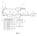
- Fig. 1 is block diagram of an exemplary uninterruptible power supply (UPS) system 10.
- UPS system 10 includes a bypass feed path 12 coupled in parallel to an inverter feed path 14 such that each path may provide power to a load 16.
- bypass feed path 12 and inverter feed path 14 are coupled to one or more power sources (not shown).
- the power source may be a utility power source or some other alternating current (AC) power source.
- bypass feed path 12 includes a Static Switch Module (not shown) implemented as a pair of anti-parallel thyristors per phase.
- Inverter feed path 14 includes a rectifier 26, an energy storage device 28, and an inverter 30.
- Rectifier 26 receives AC voltage from the power source and converts it into DC voltage.
- Inverter 30 receives the DC voltage from rectifier 26 or energy storage device 28, which may also output a DC voltage, and converts the DC voltage into an AC voltage, which is fed to load 16.
- UPS system 10 feeds load 16 using inverter feed path 14.
- UPS system 10 operates in the normal mode by closing switch (K7) 32 such that an inverter current is delivered to load 16 from the power source.
- UPS system 10 operates in bypass mode by opening switch (K7) 32 and closing the bypass static switch.
- Bypass path 12 is not ON (closed) at all times.
- UPS system 10 may also include disconnect switches (K4) 36, (K6) 38, and (Q1) 40, which may provide additional protection and/or control for UPS system 10.
- disconnect switches (K4) 36, (K6) 38, and (Q1) 40 include manual disconnects.
- energy storage device 28 is configured to bridge UPS system 10 through power interruptions.
- Energy storage device 28 may be connected directly to the DC link (in transformer-based units) or may be connected through a DC-DC (buck/boost) converter taking care of voltage adaptation.
- Energy storage device 28 is a battery or any other known form of energy storage connected to the DC link either directly or through a DC-DC conversion stage.
- UPS system 10 includes a controller 42.
- Controller 42 includes a communication component 44, a processor 46, a memory 48, storage 50, input/output (I/O) ports 52, and the like.
- Communication component 44 is a wireless or wired communication component that facilitates communication between various components (e.g., switches, rectifier, inverter) within UPS system 10.
- Processor 46 is any type of computer processor or microprocessor capable of executing computer-executable code.
- Memory 48 and storage 50 are any suitable articles of manufacture that can serve as media to store processor-executable code. These articles of manufacture represent computer-readable media (i.e., any suitable form of memory or storage) that may store the processor-executable code used by processor 46 to perform the embodiments described herein.
- controller 42 receives data related to inverter bridge currents, inverter load currents, an output AC voltage signal, bypass load currents, and bypass input voltages from any sensor suitable for the intended purpose. Using the received data, controller 42 analyzes UPS system 10 and determines whether to control rectifier 26 maintain functionality of rectifier 26 during at least one of a partial utility power outage, a full utility outage, and a failure of at least one of the rectifier legs. During normal operation, controller 42 sends signals to various components (e.g., rectifier 26, inverter 30) within UPS system 10 such that rectifier 26 converts power received from power source 20 to regulated DC power to charge energy storage device 28 as well as supply DC power to inverter 30.
- various components e.g., rectifier 26, inverter 30
- Inverter 30 may then convert the DC power to a frequency regulated (i.e., controllable) AC voltage. If at any time power source 20 fails to provide power to rectifier 26, inverter 30 may draw DC power from energy storage device 28 and may continue to supply output power to load 16.
- a frequency regulated (i.e., controllable) AC voltage If at any time power source 20 fails to provide power to rectifier 26, inverter 30 may draw DC power from energy storage device 28 and may continue to supply output power to load 16.
- Fig. 1 depicts UPS system 10 in a one-line diagram form
- the UPS system 10 may have multiple phases, such as three phases.
- the output AC power provided to the load 16 may include any number of phases (e.g., u1, u2, u3).
- any reference made herein to a current or a voltage in one phase is intended to be a reference to the current and voltage of each phase.
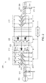
- Fig. 2 is a circuit diagram of an exemplary uninterrupted power supply (UPS) 200.
- UPS 200 is UPS system 10 (shown in Fig. 1 ).
- UPS 200 is coupled to an alternating current (AC) input source 202 that supplies three-phase power via lines 204, 206, and 208.
- AC input source 202 may represent, for example, utility power from an electrical grid or a local or remote generator.
- UPS 200 includes an input filter 210, a rectifier 212, a fourth leg 214, an inverter 216, an output filter 218, and a controller 220. Controller 220 controls operation of rectifier 212 such that rectifier 212 provides direct current (DC) power to inverter 216.
- DC direct current
- Rectifier 212 converts the three-phase AC power from AC input source 202 into DC power on a DC link 222.
- DC link 222 is a split DC link 222 and includes an upper capacitor 224 and a lower capacitor 226.
- Upper and lower capacitors 224 and 226 are coupled between positive and negative terminals of DC link 222 and filter residual AC components of the DC power on DC link 222.
- fourth leg 214 stabilizes and balances DC link 222 voltage.
- An energy storage device 228 is coupled between the positive and negative terminals of DC link 222 for storing DC power.
- DC power may be provided to inverter 216 via rectifier 212 and fourth leg 214 when AC input source 202 is ON, or via energy storage device 228 when AC input source 202 is OFF.
- Inverter 216 subsequently converts the DC power on DC link 222 into three-phase AC power on lines 230, 232, and 234. The three-phase AC power is then output to load 236.
- controller 220 is substantially similar to controller 42 (shown in Fig. 1 ) and controls operation of rectifier 212 using a processor operably coupled to memory and/or storage.
- the processor and/or other data processing circuitry may carry out instructions stored on any suitable article of manufacture having one or more tangible, machine-readable media at least collectively storing such instructions.
- the memory and/or storage may represent such articles of manufacture.
- the memory and/or the storage may represent random-access memory, read-only memory, rewriteable memory, a hard drive, or optical discs.
- controller 220 may include a field programmable gate array (FPGA) or an application-specific integrated circuit (ASIC) that has been programmed to carry out the techniques discussed herein or to support the processor (e.g., by assisting in communication).
- FPGA field programmable gate array
- ASIC application-specific integrated circuit
- controller 220 controls how rectifier 212 converts the AC power from AC input source 202 into DC power for DC link 222 by sending switching signals to a number of switches, for example, Insulated Gate Bipolar Transistors (IGBT), included within rectifier 212.
- IGBT Insulated Gate Bipolar Transistors
- controller 220 controls the amount of current passing through each of a first leg 238, a second leg 240, and a third leg 242 of rectifier 212, which in turn, controls the amount of current drawn from each phase of AC input source 202 on lines 204, 206, and 208.
- fourth leg 214 maintains a balance of DC link 222 voltage.
- Controller 220 sends switching signals to rectifier 212 at regular intervals such that each leg 238, 240, 242 of rectifier 212 draws an equal amount of current from AC input source 202, thereby providing for balanced three-phase input currents.
- controller 220 is configured to maintain functionality of rectifier 212.
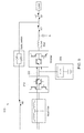
- Fig. 3 is a block diagram of an exemplary control algorithm 300 for compensating an unbalance in DC link 222 (shown in Fig. 2 ) when a component failure affects fourth leg 214 (shown in Fig. 2 ) and utility power is present.
- controller 220 (shown in Fig. 2 ) implements control algorithm 300 to control operation of rectifier 212 (shown in Fig. 2 ) to compensate for any unbalance in DC link 222 voltage in case of component failure affecting fourth leg 214 by drawing a DC component from AC input 202.
- UPS 200 shown in Fig. 2
- UPS 200 has a split DC capacitor implementation, it is important to maintain a balance of the voltage on the two-capacitor bank.
- UPS 200 is transformerless, so the DC component would be fed to the load. Because the load is connected to an AC system, it cannot be expected to handle a DC component, and such a component may disrupt the load operation causing a loss of function or even damage.
- controller 220 receives voltage measurements for upper and lower capacitors 224 and 226, and calculates a difference between the voltage measurements at a first summing junction 302. The calculated difference is input into a Udc balancing block 304.
- Rectifier 212 also performs its normal regulation of the DC link voltage.
- the voltage measurements for upper and lower capacitors 224 and 226 are summed at a second summing junction 306 to calculate a measured Udc, which represents the actual DC link voltage.
- the Udc is subtracted from a reference Udc at a third summing junction 308.
- the resultant value is applied to a Udc regulation block 310, which generates a rectifier current reference signal Iref.
- the output of Udc balancing block 304 is then summed with reference current Iref at a fourth summing junction 312 to substantially offset reference current Iref.
- the result is input to a current control block 314, which controls the draw of the DC component to be pulled from the utility power.
- Fig. 4 is an exemplary circuit diagram showing operation of first leg 238 (shown in Fig. 2 ) of rectifier 212 (shown in Fig. 2 ) when a component failure affects fourth leg 214 (shown in Fig. 2 ) and utility power is not present. If there is no utility power, rectifier 212 cannot pull DC current from the utility. When there is a power outage, or when the input voltage goes beyond a tolerance, switch (K4) 36 (shown in Fig. 1 ) of rectifier 212 is opened to isolate rectifier 212 from the utility side when the utility voltage is out of the tolerance range. By isolating rectifier 212 from the utility, the DC balancing function is assumed by one or more of rectifier legs 238, 240, and 242.
- Rectifier legs 238, 240, and 242 operate effectively as a voltage balancing circuit in the same way as fourth leg 214.
- Each of rectifier legs 238, 240, and 242 operates in substantially similar fashion, so only first rectifier leg 238 is described herein.
- first rectifier leg 238 includes an upper switch (T1) 400 and an associated antiparallel diode (D1) 402, a lower switch (T2) 404 and an associated antiparallel diode (D2) 406, a pair of antiparallel switches (T3+T4), upper capacitor 224 and lower capacitor 226 of split DC link 222 (shown in Fig. 2 ).
- First rectifier leg 238 is coupled to inductor (L2) 410 and input capacitor (Cin) 412 of input filter 210 (shown in Fig. 2 ).
- Input capacitor (Cin) 412 is positioned between upper and lower capacitors 224 and 226, and becomes charged during the energy transfer from upper capacitor 224 to lower capacitor 226.
- switch (T3) 408 is switched ON, effectively closing a path P3.
- Input capacitor (Cin) 412 then discharges, enabling another cycle to occur.
- Fig. 5 is a block diagram showing operation of an exemplary UPS 200 (shown in Fig. 2 ) having an extended rectifier input voltage range.
- controller 220 shown in Fig. 2
- controller 220 is configured to extend an input voltage tolerance range of rectifier 212 to enable rectifier 212 to operate at a lower input voltage.
- rectifier 212 can drive a higher current in low input voltage conditions.
- rectifier 212 operates at a nominal voltage with a tolerance window of +/- 15%. When voltage goes beyond the tolerance, rectifier 212 typically shuts off.
- the rectifier is a boost rectifier that boosts the input voltage to create a DC link voltage around 800V or 900V, splitting about 400V or 450V in each capacitor 224 and 226.
- Rectifier 212 regulates the DC link voltage while receiving low input voltages. Rectifier 212 operates even when the input voltage is less than -15% with respect to nominal voltage. Typical tolerances for rectifier operation are +/-10% or +/-15% with respect to nominal voltage. Rectifier 212 operates as constant power load, thereby drawing higher input current at lower voltage levels.
- rectifier 212 will hit its peak current limit at some point, and this is what determines the input voltage lower bound.
- the input voltage may be extended so that rectifier 212 can tolerate a drop of 30-40% with respect to nominal.
- rectifier 212 if rectifier 212 reaches its current limit or the power capability of rectifier 212 is insufficient, the missing energy is taken from energy storage device 228 (i.e., a battery).
- Energy storage device 228 is coupled in parallel to rectifier 212 and is configured to supplement rectifier 212 in providing energy when rectifier 212 reaches a predefined current limit.
- AC input utility and energy storage device 228 act as separate energy sources paralleled on DC link 222.
- UPS 200 By maintaining rectifier 212 operational when input voltage is lower than the tolerance, UPS 200 is prevented from reverting to battery 228 operation. However, if UPS 200 does revert to battery 228 operation, any power that from the input voltage reduces the amount of power drawn from battery 228, resulting in extended battery autonomy.
- Fig. 6 is a circuit diagram of rectifier 212 (shown in Fig. 2 ) in the event of a single-phase power outage and/or a component failure affecting a single rectifier leg. Because rectifier 212 has multiple legs 238, 240, 242, rectifier 212 can still be operational with a subset of legs 238, 240, 242 at a reduced power capability. Rectifier 212 can remain operational if one of legs 238, 240, or 242 fails or an event occurs on the input voltage that affects only one of the three phases.
- controller 220 (shown in Fig. 2 ) is configured to draw power from the remaining phases by operating second and third rectifier legs 240 and 242 as single-phase rectifiers in a four-wire distribution configuration.
- controller 220 (shown in Fig. 2 ) is configured to draw power from the remaining phases by operating second and third rectifier legs 240 and 242 as a line-to-line rectifier in a three-wire distribution configuration.
- rectifier 212 if rectifier 212 reaches its current limit or the power capability of rectifier 212 is insufficient, the missing energy is taken from energy storage device 228 (i.e., a battery).
- Energy storage device 228 is coupled in parallel to rectifier 212 and is configured to supplement rectifier 212 in providing energy when rectifier 212 reaches a predefined current limit.
- AC input utility and energy storage device 228 act as separate energy sources paralleled on DC link 222.
- rectifier 212 given the flexibility to operate rectifier 212 as three separate single-phase converters, this same principle could be used to improve efficiency by implementing adaptive capacity control. If the power requirement does not require all of the rectifier legs to be switched ON, any unnecessary rectifier legs 238, 240, and/or 242 are switched OFF to reduce losses and increase operational efficiency of rectifier 212.
- a technical effect of the systems and methods described herein includes at least one of: (a) providing a split direct current (DC) link including a first capacitor coupled between a positive DC link terminal and a first node, and a second capacitor coupled between the first node and a negative DC link terminal; (b) converting an AC voltage received from an AC source into a DC voltage to be provided to the split DC link, the AC voltage converted using at least one of a first leg, a second leg, and a third leg of a rectifier coupled to an input of the split DC link; (c) balancing the DC link voltages of the first and second capacitors using a fourth leg of the rectifier; and (d) maintaining, by a controller coupled to the rectifier, functionality of the rectifier during at least one of a partial utility power outage, a full utility power outage, and a failure of at least one of the first, second, third, and fourth legs.
- DC direct current
- the systems and methods described herein enable a four-leg rectifier to remain operational during a partial utility outage (not affecting all phases) or under failure of one converter leg.
- the systems and methods also enable extending the voltage tolerances for the rectifier operation.
- the systems and methods also enable the implementation of adaptive capacity control schemes to increase the rectifier efficiency in low-load conditions.
- the disclosed embodiments reduce stress on the rectifier and on the energy storage.
Landscapes
- Engineering & Computer Science (AREA)
- Power Engineering (AREA)
- Business, Economics & Management (AREA)
- Emergency Management (AREA)
- Stand-By Power Supply Arrangements (AREA)
- Rectifiers (AREA)
Applications Claiming Priority (1)
| Application Number | Priority Date | Filing Date | Title |
|---|---|---|---|
| US14/327,171 US10958184B2 (en) | 2014-07-09 | 2014-07-09 | Uninterruptible power supply and method of operation |
Publications (2)
| Publication Number | Publication Date |
|---|---|
| EP2966754A1 true EP2966754A1 (fr) | 2016-01-13 |
| EP2966754B1 EP2966754B1 (fr) | 2017-10-25 |
Family
ID=53496556
Family Applications (1)
| Application Number | Title | Priority Date | Filing Date |
|---|---|---|---|
| EP15174632.8A Active EP2966754B1 (fr) | 2014-07-09 | 2015-06-30 | Alimentation sans coupure et procédé de fonctionnement |
Country Status (3)
| Country | Link |
|---|---|
| US (2) | US10958184B2 (fr) |
| EP (1) | EP2966754B1 (fr) |
| CN (1) | CN105305598B (fr) |
Cited By (4)
| Publication number | Priority date | Publication date | Assignee | Title |
|---|---|---|---|---|
| EP3557745A1 (fr) * | 2018-04-17 | 2019-10-23 | ABB Schweiz AG | Procédé et système de commande permettant de compenser le courant homopolaire pour réduire le courant de masse |
| WO2020176073A1 (fr) * | 2019-02-25 | 2020-09-03 | Hewlett-Packard Development Company, L.P. | Stockage d'énergie et combinateurs de puissance à courant alternatif |
| CN113454897A (zh) * | 2019-03-27 | 2021-09-28 | Abb瑞士股份有限公司 | 模块化dc互连设备及其系统 |
| EP3989427A1 (fr) * | 2020-10-23 | 2022-04-27 | ABB Schweiz AG | Circuit de convertisseur d'alimentation électrique sans coupure |
Families Citing this family (11)
| Publication number | Priority date | Publication date | Assignee | Title |
|---|---|---|---|---|
| US10958184B2 (en) | 2014-07-09 | 2021-03-23 | Abb Schweiz Ag | Uninterruptible power supply and method of operation |
| US20160190867A1 (en) * | 2014-12-29 | 2016-06-30 | Antonio Efrain Ginart | Scalable hybrid backup energy storage system with integrated control for extended operational life |
| US10502470B2 (en) | 2016-03-22 | 2019-12-10 | Vertiv Corporation | System and method to maintain evaporator superheat during pumped refrigerant economizer operation |
| US10637279B2 (en) | 2017-02-22 | 2020-04-28 | Vertiv Corporation | Method of mitigating effects of AC input voltage surge in a transformer-less rectifier uninterruptible power supply system |
| DE102017211351A1 (de) * | 2017-07-04 | 2019-01-10 | Siemens Aktiengesellschaft | Unterbrechungsfreie Stromversorgung |
| KR101996834B1 (ko) * | 2017-09-20 | 2019-07-05 | 엘에스산전 주식회사 | 에너지 저장 시스템 |
| US11075540B2 (en) * | 2018-07-23 | 2021-07-27 | Toshiba Mitsubishi-Electric Industrial Systems Corporation | Uninterruptible power supply device |
| RU187091U1 (ru) * | 2018-12-20 | 2019-02-19 | Федеральное государственное бюджетное образовательное учреждение высшего образования "Национальный исследовательский Мордовский государственный университет им. Н.П. Огарёва" | Устройство управления трехфазным выпрямительно-инверторным модулем |
| EP4128468A1 (fr) * | 2020-05-20 | 2023-02-08 | Siemens Energy Global GmbH & Co. KG | Dispositif et procédé pour stabiliser un réseau de tension alternative |
| DE102020122458B3 (de) * | 2020-08-27 | 2022-02-03 | Keba Industrial Automation Germany Gmbh | Vorrichtung und Verfahren für den Betrieb eines Drei- oder Mehrpunktumrichters |
| CN115765389A (zh) * | 2022-10-29 | 2023-03-07 | 华为数字能源技术有限公司 | 功率变换器及其控制方法 |
Citations (3)
| Publication number | Priority date | Publication date | Assignee | Title |
|---|---|---|---|---|
| US20070228837A1 (en) * | 2006-03-31 | 2007-10-04 | American Power Conversion Corporation | Apparatus for and methods of polyphase power conversion |
| US20130258725A1 (en) * | 2012-03-29 | 2013-10-03 | General Electric Company | Systems and Methods for Balancing UPS Source Currents During Unbalanced Load Transient Conditions |
| EP2693627A2 (fr) * | 2012-07-31 | 2014-02-05 | General Electric Company | Dispositif et procédé pour un ajustage adaptif de la gradation d'un onduleur NPC dans une alimentation sans coupure sans transformateur |
Family Cites Families (14)
| Publication number | Priority date | Publication date | Assignee | Title |
|---|---|---|---|---|
| US5343079A (en) | 1991-02-25 | 1994-08-30 | Regents Of The University Of Minnesota | Standby power supply with load-current harmonics neutralizer |
| US6404655B1 (en) | 1999-12-07 | 2002-06-11 | Semikron, Inc. | Transformerless 3 phase power inverter |
| US6879053B1 (en) | 2002-10-22 | 2005-04-12 | Youtility, Inc. | Transformerless, load adaptive speed controller |
| US6950321B2 (en) | 2003-09-24 | 2005-09-27 | General Motors Corporation | Active damping control for L-C output filters in three phase four-leg inverters |
| US6924993B2 (en) | 2003-09-24 | 2005-08-02 | General Motors Corporation | Method and apparatus for controlling a stand-alone 4-leg voltage source inverter |
| FR2875970B1 (fr) * | 2004-09-27 | 2008-01-18 | Schneider Electric Ind Sas | Dispositif et procede de commande d'un convertisseur d'energie electrique et convertisseur comportant un tel dispositif |
| FR2880215B1 (fr) | 2004-12-23 | 2007-02-09 | Schneider Electric Ind Sas | Dispositif et procede de commande d'un convertisseur d'energie electrique et convertisseur comportant un tel dispositif |
| CN101001051B (zh) | 2006-01-12 | 2010-10-20 | 力博特公司 | 无输出变压器的ups |
| WO2008137276A1 (fr) * | 2007-05-08 | 2008-11-13 | Johnson Controls Technology Company | Variateur de vitesse |
| US8093746B2 (en) | 2009-12-16 | 2012-01-10 | General Electric Company | Control of four-leg transformerless uninterruptible power supply |
| US8294306B2 (en) | 2010-03-16 | 2012-10-23 | Indian Institute Of Technology Madras | DC capacitor balancing |
| US8587975B2 (en) | 2010-04-01 | 2013-11-19 | Arizona Board Of Regents For And On Behalf Of Arizona State University | PWM control of dual active bridge converters |
| CN102405588B (zh) * | 2010-05-24 | 2014-01-22 | 华为技术有限公司 | 电源方法及装置 |
| US10958184B2 (en) | 2014-07-09 | 2021-03-23 | Abb Schweiz Ag | Uninterruptible power supply and method of operation |
-
2014
- 2014-07-09 US US14/327,171 patent/US10958184B2/en active Active
-
2015
- 2015-06-30 EP EP15174632.8A patent/EP2966754B1/fr active Active
- 2015-07-09 CN CN201510400658.6A patent/CN105305598B/zh active Active
-
2021
- 2021-03-23 US US17/209,429 patent/US11539303B2/en active Active
Patent Citations (3)
| Publication number | Priority date | Publication date | Assignee | Title |
|---|---|---|---|---|
| US20070228837A1 (en) * | 2006-03-31 | 2007-10-04 | American Power Conversion Corporation | Apparatus for and methods of polyphase power conversion |
| US20130258725A1 (en) * | 2012-03-29 | 2013-10-03 | General Electric Company | Systems and Methods for Balancing UPS Source Currents During Unbalanced Load Transient Conditions |
| EP2693627A2 (fr) * | 2012-07-31 | 2014-02-05 | General Electric Company | Dispositif et procédé pour un ajustage adaptif de la gradation d'un onduleur NPC dans une alimentation sans coupure sans transformateur |
Cited By (7)
| Publication number | Priority date | Publication date | Assignee | Title |
|---|---|---|---|---|
| EP3557745A1 (fr) * | 2018-04-17 | 2019-10-23 | ABB Schweiz AG | Procédé et système de commande permettant de compenser le courant homopolaire pour réduire le courant de masse |
| US10826381B2 (en) | 2018-04-17 | 2020-11-03 | Abb Schweiz Ag | Method and control system for zero-sequence current compensation for ground current reduction |
| WO2020176073A1 (fr) * | 2019-02-25 | 2020-09-03 | Hewlett-Packard Development Company, L.P. | Stockage d'énergie et combinateurs de puissance à courant alternatif |
| CN113454897A (zh) * | 2019-03-27 | 2021-09-28 | Abb瑞士股份有限公司 | 模块化dc互连设备及其系统 |
| EP3989427A1 (fr) * | 2020-10-23 | 2022-04-27 | ABB Schweiz AG | Circuit de convertisseur d'alimentation électrique sans coupure |
| WO2022084277A1 (fr) * | 2020-10-23 | 2022-04-28 | Abb Schweiz Ag | Circuit convertisseur d'alimentation électrique sans coupure |
| US12249864B2 (en) * | 2020-10-23 | 2025-03-11 | Abb Schweiz Ag | Uninterruptible power supply converter circuit |
Also Published As
| Publication number | Publication date |
|---|---|
| US10958184B2 (en) | 2021-03-23 |
| CN105305598B (zh) | 2020-02-11 |
| CN105305598A (zh) | 2016-02-03 |
| US11539303B2 (en) | 2022-12-27 |
| US20210336551A1 (en) | 2021-10-28 |
| US20160013728A1 (en) | 2016-01-14 |
| EP2966754B1 (fr) | 2017-10-25 |
Similar Documents
| Publication | Publication Date | Title |
|---|---|---|
| US11539303B2 (en) | Uninterruptible power supply and method of operation | |
| US11929620B2 (en) | Maximizing power in a photovoltaic distributed power system | |
| US9425704B2 (en) | Power inverter with multi-fed on-board power supply for supplying a controller | |
| CN106549486A (zh) | 用于操作不间断电源的系统和方法 | |
| AU2019204315A1 (en) | DC Voltage Control In Renewable Energy Based Multilevel Power Converter | |
| US11342786B2 (en) | 3-wire multiphase UPS with bypass | |
| Zhang et al. | Interlinking modular multilevel converter of hybrid AC-DC distribution system with integrated battery energy storage | |
| US20160344233A1 (en) | Uninterruptable power supply with balancing buck/boost converter | |
| KR101027988B1 (ko) | 직렬 보상 정류기 및 이를 포함하는 직렬 보상 무정전 전원장치 | |
| US20180212471A1 (en) | An integrated multi-source ipt system | |
| Xu et al. | Evolution of single-phase power converter topologies underlining power decoupling | |
| US20190312527A1 (en) | Dc-ac converter and method of dc-ac conversion | |
| KR101647202B1 (ko) | 단상 라인 인터액티브 무정전 전원장치 | |
| Batista et al. | Proposal of three-phase two-level unidirectional SEPIC PWM rectifiers with high power factor | |
| Mastromauro et al. | DC multibus based on a single-star bridge cells modular multilevel cascade converter for dc smart grids | |
| Sousa et al. | Single-phase shunt active power filter with UPS operation using a bidirectional Dc-Dc converter for energy storage interface | |
| US20250183664A1 (en) | Systems and methods for unified power flow controller implementation | |
| RU2316875C1 (ru) | Устройство для компенсации отклонений напряжения и реактивной мощности трансформаторной подстанции | |
| Bascopé et al. | Proposal of transformerless UPS employing three state switching cell based converters | |
| Panda et al. | Modified boost inverter topology for compensation of unbalanced and nonlinear loads in three phase system | |
| Bascopé et al. | Three-phase 15kVA UPS system with power factor correction and high frequency transformer isolation | |
| Peterson et al. | Voltage sag mitigation for a high frequency multistage power conversion system | |
| Johnny | Shore supply for train maintenance using a PWM inverter in bi-directional mode | |
| WO2015198057A1 (fr) | Commande de puissance |
Legal Events
| Date | Code | Title | Description |
|---|---|---|---|
| PUAI | Public reference made under article 153(3) epc to a published international application that has entered the european phase |
Free format text: ORIGINAL CODE: 0009012 |
|
| AK | Designated contracting states |
Kind code of ref document: A1 Designated state(s): AL AT BE BG CH CY CZ DE DK EE ES FI FR GB GR HR HU IE IS IT LI LT LU LV MC MK MT NL NO PL PT RO RS SE SI SK SM TR |
|
| AX | Request for extension of the european patent |
Extension state: BA ME |
|
| 17P | Request for examination filed |
Effective date: 20160713 |
|
| RBV | Designated contracting states (corrected) |
Designated state(s): AL AT BE BG CH CY CZ DE DK EE ES FI FR GB GR HR HU IE IS IT LI LT LU LV MC MK MT NL NO PL PT RO RS SE SI SK SM TR |
|
| REG | Reference to a national code |
Ref country code: DE Ref legal event code: R079 Ref document number: 602015005532 Country of ref document: DE Free format text: PREVIOUS MAIN CLASS: H02J0009060000 Ipc: H02M0005458000 |
|
| RIC1 | Information provided on ipc code assigned before grant |
Ipc: H02J 9/06 20060101ALI20170331BHEP Ipc: H02M 7/487 20070101ALI20170331BHEP Ipc: H02M 5/458 20060101AFI20170331BHEP |
|
| GRAP | Despatch of communication of intention to grant a patent |
Free format text: ORIGINAL CODE: EPIDOSNIGR1 |
|
| INTG | Intention to grant announced |
Effective date: 20170516 |
|
| GRAS | Grant fee paid |
Free format text: ORIGINAL CODE: EPIDOSNIGR3 |
|
| GRAA | (expected) grant |
Free format text: ORIGINAL CODE: 0009210 |
|
| AK | Designated contracting states |
Kind code of ref document: B1 Designated state(s): AL AT BE BG CH CY CZ DE DK EE ES FI FR GB GR HR HU IE IS IT LI LT LU LV MC MK MT NL NO PL PT RO RS SE SI SK SM TR |
|
| REG | Reference to a national code |
Ref country code: GB Ref legal event code: FG4D |
|
| REG | Reference to a national code |
Ref country code: CH Ref legal event code: EP |
|
| REG | Reference to a national code |
Ref country code: AT Ref legal event code: REF Ref document number: 940778 Country of ref document: AT Kind code of ref document: T Effective date: 20171115 |
|
| REG | Reference to a national code |
Ref country code: IE Ref legal event code: FG4D |
|
| REG | Reference to a national code |
Ref country code: DE Ref legal event code: R096 Ref document number: 602015005532 Country of ref document: DE |
|
| REG | Reference to a national code |
Ref country code: NL Ref legal event code: MP Effective date: 20171025 |
|
| REG | Reference to a national code |
Ref country code: LT Ref legal event code: MG4D |
|
| REG | Reference to a national code |
Ref country code: AT Ref legal event code: MK05 Ref document number: 940778 Country of ref document: AT Kind code of ref document: T Effective date: 20171025 |
|
| PG25 | Lapsed in a contracting state [announced via postgrant information from national office to epo] |
Ref country code: NL Free format text: LAPSE BECAUSE OF FAILURE TO SUBMIT A TRANSLATION OF THE DESCRIPTION OR TO PAY THE FEE WITHIN THE PRESCRIBED TIME-LIMIT Effective date: 20171025 |
|
| PG25 | Lapsed in a contracting state [announced via postgrant information from national office to epo] |
Ref country code: LT Free format text: LAPSE BECAUSE OF FAILURE TO SUBMIT A TRANSLATION OF THE DESCRIPTION OR TO PAY THE FEE WITHIN THE PRESCRIBED TIME-LIMIT Effective date: 20171025 Ref country code: FI Free format text: LAPSE BECAUSE OF FAILURE TO SUBMIT A TRANSLATION OF THE DESCRIPTION OR TO PAY THE FEE WITHIN THE PRESCRIBED TIME-LIMIT Effective date: 20171025 Ref country code: SE Free format text: LAPSE BECAUSE OF FAILURE TO SUBMIT A TRANSLATION OF THE DESCRIPTION OR TO PAY THE FEE WITHIN THE PRESCRIBED TIME-LIMIT Effective date: 20171025 Ref country code: ES Free format text: LAPSE BECAUSE OF FAILURE TO SUBMIT A TRANSLATION OF THE DESCRIPTION OR TO PAY THE FEE WITHIN THE PRESCRIBED TIME-LIMIT Effective date: 20171025 Ref country code: NO Free format text: LAPSE BECAUSE OF FAILURE TO SUBMIT A TRANSLATION OF THE DESCRIPTION OR TO PAY THE FEE WITHIN THE PRESCRIBED TIME-LIMIT Effective date: 20180125 |
|
| PG25 | Lapsed in a contracting state [announced via postgrant information from national office to epo] |
Ref country code: IS Free format text: LAPSE BECAUSE OF FAILURE TO SUBMIT A TRANSLATION OF THE DESCRIPTION OR TO PAY THE FEE WITHIN THE PRESCRIBED TIME-LIMIT Effective date: 20180225 Ref country code: AT Free format text: LAPSE BECAUSE OF FAILURE TO SUBMIT A TRANSLATION OF THE DESCRIPTION OR TO PAY THE FEE WITHIN THE PRESCRIBED TIME-LIMIT Effective date: 20171025 Ref country code: RS Free format text: LAPSE BECAUSE OF FAILURE TO SUBMIT A TRANSLATION OF THE DESCRIPTION OR TO PAY THE FEE WITHIN THE PRESCRIBED TIME-LIMIT Effective date: 20171025 Ref country code: HR Free format text: LAPSE BECAUSE OF FAILURE TO SUBMIT A TRANSLATION OF THE DESCRIPTION OR TO PAY THE FEE WITHIN THE PRESCRIBED TIME-LIMIT Effective date: 20171025 Ref country code: BG Free format text: LAPSE BECAUSE OF FAILURE TO SUBMIT A TRANSLATION OF THE DESCRIPTION OR TO PAY THE FEE WITHIN THE PRESCRIBED TIME-LIMIT Effective date: 20180125 Ref country code: GR Free format text: LAPSE BECAUSE OF FAILURE TO SUBMIT A TRANSLATION OF THE DESCRIPTION OR TO PAY THE FEE WITHIN THE PRESCRIBED TIME-LIMIT Effective date: 20180126 Ref country code: LV Free format text: LAPSE BECAUSE OF FAILURE TO SUBMIT A TRANSLATION OF THE DESCRIPTION OR TO PAY THE FEE WITHIN THE PRESCRIBED TIME-LIMIT Effective date: 20171025 |
|
| REG | Reference to a national code |
Ref country code: FR Ref legal event code: PLFP Year of fee payment: 4 |
|
| REG | Reference to a national code |
Ref country code: DE Ref legal event code: R097 Ref document number: 602015005532 Country of ref document: DE |
|
| PG25 | Lapsed in a contracting state [announced via postgrant information from national office to epo] |
Ref country code: SK Free format text: LAPSE BECAUSE OF FAILURE TO SUBMIT A TRANSLATION OF THE DESCRIPTION OR TO PAY THE FEE WITHIN THE PRESCRIBED TIME-LIMIT Effective date: 20171025 Ref country code: EE Free format text: LAPSE BECAUSE OF FAILURE TO SUBMIT A TRANSLATION OF THE DESCRIPTION OR TO PAY THE FEE WITHIN THE PRESCRIBED TIME-LIMIT Effective date: 20171025 Ref country code: CY Free format text: LAPSE BECAUSE OF FAILURE TO SUBMIT A TRANSLATION OF THE DESCRIPTION OR TO PAY THE FEE WITHIN THE PRESCRIBED TIME-LIMIT Effective date: 20171025 Ref country code: DK Free format text: LAPSE BECAUSE OF FAILURE TO SUBMIT A TRANSLATION OF THE DESCRIPTION OR TO PAY THE FEE WITHIN THE PRESCRIBED TIME-LIMIT Effective date: 20171025 Ref country code: CZ Free format text: LAPSE BECAUSE OF FAILURE TO SUBMIT A TRANSLATION OF THE DESCRIPTION OR TO PAY THE FEE WITHIN THE PRESCRIBED TIME-LIMIT Effective date: 20171025 |
|
| PG25 | Lapsed in a contracting state [announced via postgrant information from national office to epo] |
Ref country code: SM Free format text: LAPSE BECAUSE OF FAILURE TO SUBMIT A TRANSLATION OF THE DESCRIPTION OR TO PAY THE FEE WITHIN THE PRESCRIBED TIME-LIMIT Effective date: 20171025 Ref country code: PL Free format text: LAPSE BECAUSE OF FAILURE TO SUBMIT A TRANSLATION OF THE DESCRIPTION OR TO PAY THE FEE WITHIN THE PRESCRIBED TIME-LIMIT Effective date: 20171025 Ref country code: IT Free format text: LAPSE BECAUSE OF FAILURE TO SUBMIT A TRANSLATION OF THE DESCRIPTION OR TO PAY THE FEE WITHIN THE PRESCRIBED TIME-LIMIT Effective date: 20171025 Ref country code: RO Free format text: LAPSE BECAUSE OF FAILURE TO SUBMIT A TRANSLATION OF THE DESCRIPTION OR TO PAY THE FEE WITHIN THE PRESCRIBED TIME-LIMIT Effective date: 20171025 |
|
| PLBE | No opposition filed within time limit |
Free format text: ORIGINAL CODE: 0009261 |
|
| STAA | Information on the status of an ep patent application or granted ep patent |
Free format text: STATUS: NO OPPOSITION FILED WITHIN TIME LIMIT |
|
| 26N | No opposition filed |
Effective date: 20180726 |
|
| PG25 | Lapsed in a contracting state [announced via postgrant information from national office to epo] |
Ref country code: SI Free format text: LAPSE BECAUSE OF FAILURE TO SUBMIT A TRANSLATION OF THE DESCRIPTION OR TO PAY THE FEE WITHIN THE PRESCRIBED TIME-LIMIT Effective date: 20171025 |
|
| REG | Reference to a national code |
Ref country code: BE Ref legal event code: MM Effective date: 20180630 |
|
| PG25 | Lapsed in a contracting state [announced via postgrant information from national office to epo] |
Ref country code: LU Free format text: LAPSE BECAUSE OF NON-PAYMENT OF DUE FEES Effective date: 20180630 Ref country code: MC Free format text: LAPSE BECAUSE OF FAILURE TO SUBMIT A TRANSLATION OF THE DESCRIPTION OR TO PAY THE FEE WITHIN THE PRESCRIBED TIME-LIMIT Effective date: 20171025 |
|
| REG | Reference to a national code |
Ref country code: IE Ref legal event code: MM4A |
|
| PG25 | Lapsed in a contracting state [announced via postgrant information from national office to epo] |
Ref country code: IE Free format text: LAPSE BECAUSE OF NON-PAYMENT OF DUE FEES Effective date: 20180630 |
|
| PG25 | Lapsed in a contracting state [announced via postgrant information from national office to epo] |
Ref country code: BE Free format text: LAPSE BECAUSE OF NON-PAYMENT OF DUE FEES Effective date: 20180630 |
|
| PG25 | Lapsed in a contracting state [announced via postgrant information from national office to epo] |
Ref country code: MT Free format text: LAPSE BECAUSE OF NON-PAYMENT OF DUE FEES Effective date: 20180630 |
|
| PG25 | Lapsed in a contracting state [announced via postgrant information from national office to epo] |
Ref country code: TR Free format text: LAPSE BECAUSE OF FAILURE TO SUBMIT A TRANSLATION OF THE DESCRIPTION OR TO PAY THE FEE WITHIN THE PRESCRIBED TIME-LIMIT Effective date: 20171025 |
|
| PG25 | Lapsed in a contracting state [announced via postgrant information from national office to epo] |
Ref country code: PT Free format text: LAPSE BECAUSE OF FAILURE TO SUBMIT A TRANSLATION OF THE DESCRIPTION OR TO PAY THE FEE WITHIN THE PRESCRIBED TIME-LIMIT Effective date: 20171025 |
|
| PG25 | Lapsed in a contracting state [announced via postgrant information from national office to epo] |
Ref country code: MK Free format text: LAPSE BECAUSE OF NON-PAYMENT OF DUE FEES Effective date: 20171025 Ref country code: HU Free format text: LAPSE BECAUSE OF FAILURE TO SUBMIT A TRANSLATION OF THE DESCRIPTION OR TO PAY THE FEE WITHIN THE PRESCRIBED TIME-LIMIT; INVALID AB INITIO Effective date: 20150630 |
|
| PG25 | Lapsed in a contracting state [announced via postgrant information from national office to epo] |
Ref country code: AL Free format text: LAPSE BECAUSE OF FAILURE TO SUBMIT A TRANSLATION OF THE DESCRIPTION OR TO PAY THE FEE WITHIN THE PRESCRIBED TIME-LIMIT Effective date: 20171025 |
|
| REG | Reference to a national code |
Ref country code: DE Ref legal event code: R081 Ref document number: 602015005532 Country of ref document: DE Owner name: ABB SCHWEIZ AG, CH Free format text: FORMER OWNER: GENERAL ELECTRIC COMPANY, SCHENECTADY, N.Y., US Ref country code: DE Ref legal event code: R081 Ref document number: 602015005532 Country of ref document: DE Owner name: ABB SCHWEIZ AG, CH Free format text: FORMER OWNER: GENERAL ELECTRIC COMPANY, SCHENECTADY, NY, US |
|
| PGFP | Annual fee paid to national office [announced via postgrant information from national office to epo] |
Ref country code: DE Payment date: 20250618 Year of fee payment: 11 |
|
| PGFP | Annual fee paid to national office [announced via postgrant information from national office to epo] |
Ref country code: GB Payment date: 20250618 Year of fee payment: 11 |
|
| REG | Reference to a national code |
Ref country code: DE Ref legal event code: R082 Ref document number: 602015005532 Country of ref document: DE Representative=s name: ZIMMERMANN & PARTNER PATENTANWAELTE MBB, DE |
|
| PGFP | Annual fee paid to national office [announced via postgrant information from national office to epo] |
Ref country code: FR Payment date: 20250625 Year of fee payment: 11 |
|
| PGFP | Annual fee paid to national office [announced via postgrant information from national office to epo] |
Ref country code: CH Payment date: 20250701 Year of fee payment: 11 |