EP2975366A1 - Energiesystemüberwachung - Google Patents
Energiesystemüberwachung Download PDFInfo
- Publication number
- EP2975366A1 EP2975366A1 EP15174916.5A EP15174916A EP2975366A1 EP 2975366 A1 EP2975366 A1 EP 2975366A1 EP 15174916 A EP15174916 A EP 15174916A EP 2975366 A1 EP2975366 A1 EP 2975366A1
- Authority
- EP
- European Patent Office
- Prior art keywords
- optical
- light
- wavelength
- output
- sensor
- Prior art date
- Legal status (The legal status is an assumption and is not a legal conclusion. Google has not performed a legal analysis and makes no representation as to the accuracy of the status listed.)
- Granted
Links
Images






Classifications
-
- G—PHYSICS
- G01—MEASURING; TESTING
- G01D—MEASURING NOT SPECIALLY ADAPTED FOR A SPECIFIC VARIABLE; ARRANGEMENTS FOR MEASURING TWO OR MORE VARIABLES NOT COVERED IN A SINGLE OTHER SUBCLASS; TARIFF METERING APPARATUS; MEASURING OR TESTING NOT OTHERWISE PROVIDED FOR
- G01D5/00—Mechanical means for transferring the output of a sensing member; Means for converting the output of a sensing member to another variable where the form or nature of the sensing member does not constrain the means for converting; Transducers not specially adapted for a specific variable
- G01D5/26—Mechanical means for transferring the output of a sensing member; Means for converting the output of a sensing member to another variable where the form or nature of the sensing member does not constrain the means for converting; Transducers not specially adapted for a specific variable characterised by optical transfer means, i.e. using infrared, visible, or ultraviolet light
- G01D5/32—Mechanical means for transferring the output of a sensing member; Means for converting the output of a sensing member to another variable where the form or nature of the sensing member does not constrain the means for converting; Transducers not specially adapted for a specific variable characterised by optical transfer means, i.e. using infrared, visible, or ultraviolet light with attenuation or whole or partial obturation of beams of light
- G01D5/34—Mechanical means for transferring the output of a sensing member; Means for converting the output of a sensing member to another variable where the form or nature of the sensing member does not constrain the means for converting; Transducers not specially adapted for a specific variable characterised by optical transfer means, i.e. using infrared, visible, or ultraviolet light with attenuation or whole or partial obturation of beams of light the beams of light being detected by photocells
- G01D5/353—Mechanical means for transferring the output of a sensing member; Means for converting the output of a sensing member to another variable where the form or nature of the sensing member does not constrain the means for converting; Transducers not specially adapted for a specific variable characterised by optical transfer means, i.e. using infrared, visible, or ultraviolet light with attenuation or whole or partial obturation of beams of light the beams of light being detected by photocells influencing the transmission properties of an optical fibre
- G01D5/35383—Mechanical means for transferring the output of a sensing member; Means for converting the output of a sensing member to another variable where the form or nature of the sensing member does not constrain the means for converting; Transducers not specially adapted for a specific variable characterised by optical transfer means, i.e. using infrared, visible, or ultraviolet light with attenuation or whole or partial obturation of beams of light the beams of light being detected by photocells influencing the transmission properties of an optical fibre using multiple sensor devices using multiplexing techniques
-
- G—PHYSICS
- G01—MEASURING; TESTING
- G01D—MEASURING NOT SPECIALLY ADAPTED FOR A SPECIFIC VARIABLE; ARRANGEMENTS FOR MEASURING TWO OR MORE VARIABLES NOT COVERED IN A SINGLE OTHER SUBCLASS; TARIFF METERING APPARATUS; MEASURING OR TESTING NOT OTHERWISE PROVIDED FOR
- G01D5/00—Mechanical means for transferring the output of a sensing member; Means for converting the output of a sensing member to another variable where the form or nature of the sensing member does not constrain the means for converting; Transducers not specially adapted for a specific variable
- G01D5/26—Mechanical means for transferring the output of a sensing member; Means for converting the output of a sensing member to another variable where the form or nature of the sensing member does not constrain the means for converting; Transducers not specially adapted for a specific variable characterised by optical transfer means, i.e. using infrared, visible, or ultraviolet light
- G01D5/32—Mechanical means for transferring the output of a sensing member; Means for converting the output of a sensing member to another variable where the form or nature of the sensing member does not constrain the means for converting; Transducers not specially adapted for a specific variable characterised by optical transfer means, i.e. using infrared, visible, or ultraviolet light with attenuation or whole or partial obturation of beams of light
- G01D5/34—Mechanical means for transferring the output of a sensing member; Means for converting the output of a sensing member to another variable where the form or nature of the sensing member does not constrain the means for converting; Transducers not specially adapted for a specific variable characterised by optical transfer means, i.e. using infrared, visible, or ultraviolet light with attenuation or whole or partial obturation of beams of light the beams of light being detected by photocells
- G01D5/353—Mechanical means for transferring the output of a sensing member; Means for converting the output of a sensing member to another variable where the form or nature of the sensing member does not constrain the means for converting; Transducers not specially adapted for a specific variable characterised by optical transfer means, i.e. using infrared, visible, or ultraviolet light with attenuation or whole or partial obturation of beams of light the beams of light being detected by photocells influencing the transmission properties of an optical fibre
- G01D5/35306—Mechanical means for transferring the output of a sensing member; Means for converting the output of a sensing member to another variable where the form or nature of the sensing member does not constrain the means for converting; Transducers not specially adapted for a specific variable characterised by optical transfer means, i.e. using infrared, visible, or ultraviolet light with attenuation or whole or partial obturation of beams of light the beams of light being detected by photocells influencing the transmission properties of an optical fibre using an interferometer arrangement
- G01D5/35309—Mechanical means for transferring the output of a sensing member; Means for converting the output of a sensing member to another variable where the form or nature of the sensing member does not constrain the means for converting; Transducers not specially adapted for a specific variable characterised by optical transfer means, i.e. using infrared, visible, or ultraviolet light with attenuation or whole or partial obturation of beams of light the beams of light being detected by photocells influencing the transmission properties of an optical fibre using an interferometer arrangement using multiple waves interferometer
- G01D5/35316—Mechanical means for transferring the output of a sensing member; Means for converting the output of a sensing member to another variable where the form or nature of the sensing member does not constrain the means for converting; Transducers not specially adapted for a specific variable characterised by optical transfer means, i.e. using infrared, visible, or ultraviolet light with attenuation or whole or partial obturation of beams of light the beams of light being detected by photocells influencing the transmission properties of an optical fibre using an interferometer arrangement using multiple waves interferometer using a Bragg gratings
-
- G—PHYSICS
- G01—MEASURING; TESTING
- G01D—MEASURING NOT SPECIALLY ADAPTED FOR A SPECIFIC VARIABLE; ARRANGEMENTS FOR MEASURING TWO OR MORE VARIABLES NOT COVERED IN A SINGLE OTHER SUBCLASS; TARIFF METERING APPARATUS; MEASURING OR TESTING NOT OTHERWISE PROVIDED FOR
- G01D5/00—Mechanical means for transferring the output of a sensing member; Means for converting the output of a sensing member to another variable where the form or nature of the sensing member does not constrain the means for converting; Transducers not specially adapted for a specific variable
- G01D5/26—Mechanical means for transferring the output of a sensing member; Means for converting the output of a sensing member to another variable where the form or nature of the sensing member does not constrain the means for converting; Transducers not specially adapted for a specific variable characterised by optical transfer means, i.e. using infrared, visible, or ultraviolet light
- G01D5/32—Mechanical means for transferring the output of a sensing member; Means for converting the output of a sensing member to another variable where the form or nature of the sensing member does not constrain the means for converting; Transducers not specially adapted for a specific variable characterised by optical transfer means, i.e. using infrared, visible, or ultraviolet light with attenuation or whole or partial obturation of beams of light
- G01D5/34—Mechanical means for transferring the output of a sensing member; Means for converting the output of a sensing member to another variable where the form or nature of the sensing member does not constrain the means for converting; Transducers not specially adapted for a specific variable characterised by optical transfer means, i.e. using infrared, visible, or ultraviolet light with attenuation or whole or partial obturation of beams of light the beams of light being detected by photocells
- G01D5/353—Mechanical means for transferring the output of a sensing member; Means for converting the output of a sensing member to another variable where the form or nature of the sensing member does not constrain the means for converting; Transducers not specially adapted for a specific variable characterised by optical transfer means, i.e. using infrared, visible, or ultraviolet light with attenuation or whole or partial obturation of beams of light the beams of light being detected by photocells influencing the transmission properties of an optical fibre
- G01D5/35383—Mechanical means for transferring the output of a sensing member; Means for converting the output of a sensing member to another variable where the form or nature of the sensing member does not constrain the means for converting; Transducers not specially adapted for a specific variable characterised by optical transfer means, i.e. using infrared, visible, or ultraviolet light with attenuation or whole or partial obturation of beams of light the beams of light being detected by photocells influencing the transmission properties of an optical fibre using multiple sensor devices using multiplexing techniques
- G01D5/3539—Mechanical means for transferring the output of a sensing member; Means for converting the output of a sensing member to another variable where the form or nature of the sensing member does not constrain the means for converting; Transducers not specially adapted for a specific variable characterised by optical transfer means, i.e. using infrared, visible, or ultraviolet light with attenuation or whole or partial obturation of beams of light the beams of light being detected by photocells influencing the transmission properties of an optical fibre using multiple sensor devices using multiplexing techniques using time division multiplexing
-
- G—PHYSICS
- G01—MEASURING; TESTING
- G01L—MEASURING FORCE, STRESS, TORQUE, WORK, MECHANICAL POWER, MECHANICAL EFFICIENCY, OR FLUID PRESSURE
- G01L1/00—Measuring force or stress, in general
- G01L1/24—Measuring force or stress, in general by measuring variations of optical properties of material when it is stressed, e.g. by photoelastic stress analysis using infrared, visible light, ultraviolet
- G01L1/242—Measuring force or stress, in general by measuring variations of optical properties of material when it is stressed, e.g. by photoelastic stress analysis using infrared, visible light, ultraviolet the material being an optical fibre
- G01L1/246—Measuring force or stress, in general by measuring variations of optical properties of material when it is stressed, e.g. by photoelastic stress analysis using infrared, visible light, ultraviolet the material being an optical fibre using integrated gratings, e.g. Bragg gratings
-
- G—PHYSICS
- G01—MEASURING; TESTING
- G01R—MEASURING ELECTRIC VARIABLES; MEASURING MAGNETIC VARIABLES
- G01R31/00—Arrangements for testing electric properties; Arrangements for locating electric faults; Arrangements for electrical testing characterised by what is being tested not provided for elsewhere
- G01R31/36—Arrangements for testing, measuring or monitoring the electrical condition of accumulators or electric batteries, e.g. capacity or state of charge [SoC]
- G01R31/382—Arrangements for monitoring battery or accumulator variables, e.g. SoC
-
- G—PHYSICS
- G02—OPTICS
- G02B—OPTICAL ELEMENTS, SYSTEMS OR APPARATUS
- G02B6/00—Light guides; Structural details of arrangements comprising light guides and other optical elements, e.g. couplings
- G02B6/10—Light guides; Structural details of arrangements comprising light guides and other optical elements, e.g. couplings of the optical waveguide type
- G02B6/12—Light guides; Structural details of arrangements comprising light guides and other optical elements, e.g. couplings of the optical waveguide type of the integrated circuit kind
- G02B6/12007—Light guides; Structural details of arrangements comprising light guides and other optical elements, e.g. couplings of the optical waveguide type of the integrated circuit kind forming wavelength selective elements, e.g. multiplexer, demultiplexer
- G02B6/12009—Light guides; Structural details of arrangements comprising light guides and other optical elements, e.g. couplings of the optical waveguide type of the integrated circuit kind forming wavelength selective elements, e.g. multiplexer, demultiplexer comprising arrayed waveguide grating [AWG] devices, i.e. with a phased array of waveguides
-
- G—PHYSICS
- G02—OPTICS
- G02B—OPTICAL ELEMENTS, SYSTEMS OR APPARATUS
- G02B6/00—Light guides; Structural details of arrangements comprising light guides and other optical elements, e.g. couplings
- G02B6/24—Coupling light guides
- G02B6/26—Optical coupling means
- G02B6/28—Optical coupling means having data bus means, i.e. plural waveguides interconnected and providing an inherently bidirectional system by mixing and splitting signals
- G02B6/293—Optical coupling means having data bus means, i.e. plural waveguides interconnected and providing an inherently bidirectional system by mixing and splitting signals with wavelength selective means
- G02B6/29379—Optical coupling means having data bus means, i.e. plural waveguides interconnected and providing an inherently bidirectional system by mixing and splitting signals with wavelength selective means characterised by the function or use of the complete device
- G02B6/2938—Optical coupling means having data bus means, i.e. plural waveguides interconnected and providing an inherently bidirectional system by mixing and splitting signals with wavelength selective means characterised by the function or use of the complete device for multiplexing or demultiplexing, i.e. combining or separating wavelengths, e.g. 1xN, NxM
-
- G—PHYSICS
- G01—MEASURING; TESTING
- G01N—INVESTIGATING OR ANALYSING MATERIALS BY DETERMINING THEIR CHEMICAL OR PHYSICAL PROPERTIES
- G01N2201/00—Features of devices classified in G01N21/00
- G01N2201/08—Optical fibres; light guides
- G01N2201/088—Using a sensor fibre
Definitions
- This application relates generally to techniques for monitoring and/or managing systems, including energy storage and/or power generation systems.
- the application also relates to components, devices, systems, and methods pertaining to such techniques.
- Various embodiments described herein involve systems and methods for monitoring and/or managing systems, such as energy storage devices, power generation systems and other such devices and systems.
- Some embodiments involve an optical monitoring system that can be used to monitor an energy system.
- the monitoring system includes N > 1 optical sensors. Each optical sensor emanates output light in response to input light, the output light having a centroid wavelength that changes in response to a sensed parameter.
- the output light of the optical sensors is optically coupled to the input waveguide and the optical coupler spatially disperses the light from the input waveguide according to wavelength.
- the output light emanating from each optical sensor is optically coupled through at least one output waveguide to a photodetector.
- the electrical signal generated by the photodetector in response to the sensor output light provides information about the sensed parameter.
- Embodiments described in this disclosure involve optically-based monitoring and management systems. Such systems may be particularly useful for monitoring and/or managing energy devices and/or systems that generate, store and/or distribute energy.
- the approaches disclosed herein enable comprehensive real-time performance monitoring and management of these systems, reducing the need for overdesign of energy systems.
- the monitoring systems of the present disclosure combine fiber optic sensors to sense internal and/or external parameters of the energy system. The sensed information may be used by smart algorithms to infer and/or predict energy system state and to provide feedback for energy system management.
- the approaches disclosed herein can be used to monitor and/or manage a variety of systems, but are particularly applicable to modularized systems such as batteries and battery packs, fuel cell stacks, turbine-based power systems, solar arrays, and other types of energy storage and power generation devices and systems.
- FIG. 1 is a block diagram of a monitoring and management system (MMS) 100.
- MMS monitoring and management system
- Multiple internal optical sensors, S1, S2, ... SN are arranged to sense multiple internal properties of the battery 101.
- the optical sensors S1, S2, ... SN may be disposed within the battery 101 and configured to measure one or more internal battery parameters such as internal temperature, stress, strain, acoustic emission, ion concentration, chemistry, presence and/or concentration of gas, and/or other internal parameters of the battery 101.
- sensors S1, S2, ... SN are each configured to sense the same parameter.
- the outputs of multiple sensors that sense the same parameter may be combined to yield an average or composite value for the sensed parameter.
- multiple sensors that sense the same parameter can be used to develop a map of the spatial distribution of the parameter in the interior and/or at the exterior of the battery 101.
- optical sensors S1, S2, ... SN are disposed on one or more sensor waveguides (shown in FIG. 1 as a single fiber optic (FO) cable 130) and are embedded within a battery 101.
- Each of the sensors S1, S2, ... SN may operate within a different wavelength band from other sensors on the FO cable 130.
- sensor S1 may operate within a first wavelength band centered at wavelength ⁇ 1
- sensor S2 may operate within a second wavelength band centered at ⁇ 2
- sensor SN may operate within an Nth wavelength band centered at ⁇ N .
- Each wavelength band ⁇ 1 , ⁇ 2 , .. ⁇ N may be selected so that it does not substantially overlap with the wavelength bands of the other sensors.
- the optical sensors S1, S2, ... SN are optically coupled to a light source 110, which may be a broadband light source that supplies excitation light across a broad wavelength band that spans the operating wavelength bands of the optical sensors S1, S2, ... SN.
- Output light from optical sensors S1, S2, ... SN is carried on sensor waveguide fiber optic cable 130 to an input waveguide 141 of an optical coupler 140.
- the optical coupler 140 is a wavelength domain optical demultiplexer that spatially disperses light from the input waveguide 141 to multiple output waveguides 142 according to the wavelength of the light.
- the optical coupler may comprise a linear variable transmission structure and/or an arrayed waveguide grating, for example.
- the output waveguides 142 are optically coupled to a digitizer 150 that may include multiple photodetectors. Each photodetector is configured to generate an electrical signal in response to light that falls on a light sensitive surface of the photodetector.
- the electrical signals generated by the photodetectors of the digitizer 150 include information from the sensors S1, S2, ... SN about the sensed parameters. The information can be used by the monitoring/management processor 160 to determine the state of the battery 101 and/or to provide feedback to control battery operations.
- the system includes at least N photodetectors. In some implementations, the system includes at least N pairs of photodetectors. These implementations are discussed in more detail below.
- An additional photodetector may be used to monitor intensity of the input light, e.g., by tapping off the input waveguide 141.
- the management processor 160 may be configured to implement various processes that affect battery status based on the information provided by the sensors. According to various implementations, some aspects of the battery operation, e.g., charge rate and/or charge cycles, may be automatically controlled through a feedback output 161 from the management processor 160.
- the management processor 160 may use sensor information to make predictions and/or estimations regarding the state of the battery, e.g., state of health (SOH) and/or state of charge (SOC). These predictions and estimations may be developed using theoretical and/ or empirical models and may be adaptable based on operational conditions of the battery, measures of internal and/or external parameters and/or correlations between the operational conditions and measured parameters. Some implementations may provide energy system monitoring only and thus may not include the management system components, and/or in some implementations the management system may not provide feedback to the energy system.
- SOH state of health
- SOC state of charge
- information acquired or developed by the management processor 160 may be provided to an operator via an electronic or printed report.
- the management processor 160 may compile, analyze, trend, and/or summarize the sensed parameters, and/or may perform other processes using the sensed parameters as input, such as predicting and/or estimating the state of the energy system 101.
- the results of these processes and/or other information derived from monitoring the energy system 101 may be provided in a report that can be displayed graphically or textually or in any convenient form to an operator and/or may be provided to another computer system for storage in a database and/or further analysis.
- the sensors S1, S2, ... SN disposed on the FO cable130 may comprise any type (or multiple types) of optical sensor, including fiber Bragg grating (FBG) sensors and/or etalon or Fabry-Perot (FP) sensors. Both the FBG and etalon/FP sensors are collectively referred to herein as optical sensors. Although some examples provided below are based on FBG sensors, it will be understood that other types of optical sensors could alternatively or additionally be used in these and other embodiments.
- FBG fiber Bragg grating
- FP Fabry-Perot
- light from the light source 110 travels through the FO cable 130 to the sensors S1, S2, ... SN.
- the input light interacts with the FBG sensors S1, S2, ... SN that are spaced apart along the FO cable 130.
- Each FBG sensor reflects a portion of the input light, and the reflected light is referred to as output light emanating from the optical sensor.
- the output light from all sensors travels through the FO 130 to the input waveguide 141 of the optical demultiplexer 140.
- the FBG sensors can be formed by a periodic modulation of the refractive index along a finite length (typically a few mm) of the core of the FO cable. This pattern reflects a wavelength, called the Bragg wavelength,that is determined by the periodicity of the refractive index profile of the FBG sensor. In practice, the sensor typically reflects a narrow band of wavelengths centered at the Bragg wavelength.
- the Bragg wavelength at a characteristic or base value of the external stimulus is denoted ⁇ , and light having a peak, center, or centroid wavelength ⁇ (and a narrow band of wavelengths near ⁇ ) is reflected from the sensor when it is in a predetermined base condition.
- the base condition may correspond to 25 degrees C and/or zero strain.
- the stimulus When the sensor is subjected to an external stimulus, such as temperature, strain, or other such stimulus, the stimulus changes the periodicity of the grating and the index of refraction of the FBG, and thereby alters the reflected light so that the reflected light has a peak, center, or centroid wavelength, ⁇ s , different from the base wavelength, ⁇ .
- the resulting wavelength shift, ⁇ / ⁇ ( ⁇ - ⁇ s )/ ⁇ is a proxy measure of the stimulus.
- FBG sensors may be sensitive to changes in refractive index n, strain ⁇ 1 , and ambient temperature changes ⁇ T, for example.
- the refractive index n can be made sensitive to the chemical environment of the sensor by stripping the FO cladding over the sensor element region and/or by adding appropriate coatings to this sensitive area.
- FBG sensors can be made sensitive to the chemical environment by applying special coatings that convert the chemical composition of the environment into a strain signal (e.g. hydrogen sensors based on palladium coatings).
- optical sensors such as FBG sensors are used to detect chemical composition changes in battery cells that might affect performance. An example of this is formation of a corrosive agent, hydrogen fluoride (HF), in Li-ion cells caused by moisture penetration.
- HF hydrogen fluoride
- FBGs The sensitivity of FBGs to temperature changes allows local temperatures within battery cells to be monitored. While this is useful in general for battery system management, it is particularly beneficial for early detection of thermal runaways.
- Thermal runaways affect many battery chemistries and can be devastating in Lithium-ion cells due to their high energy density.
- the high heat of the failing cell can propagate to the next cell, causing it to become thermally unstable as well.
- a chain reaction occurs in which each cell disintegrates at its own timetable.
- a pack of battery cells can be destroyed within a few seconds or can linger on for several hours as each cell is consumed one-by-one.
- the sensitivity of the FBG sensors to strain allows embedding FBG sensors into battery electrodes to monitor the expansion/contraction cycles of the electrodes (which is useful for estimating charge levels, e.g. in Lithium-ion cells). Additionally, electrode strain measurements allow for examining the degradation of the electrodes, and thus the overall degradation of the battery. FBG sensitivity to strain also allows measurement of internal cell pressure by capturing cell wall strains.
- a multi-sensor configuration may be used so that the parameter of interest can be compensated for the contributions of other parameters.
- a two-sensor approach may be used for temperature-compensated chemical sensing, where the two sensors can be arranged in close proximity.
- a first sensor of the two sensors is exposed to temperature and is also exposed to the chemical environment by stripping its cladding.
- a second sensor of the two sensors used for compensation retains its cladding and is only sensitive to temperature. Similar configurations may be used for temperature-compensated strain measurements and strain-compensated temperature measurements.
- two FBG sensors are placed in close proximity where the first sensor is exposed to strain and temperature and a second sensor used for compensation is exposed to temperature but not strain.
- the temperature measurement of the second sensor is used to compensate for temperature-induced changes in the reflected wavelength of the first sensor.
- the first sensor may be placed within an electrode or cell wall of a battery and the second sensor may be placed nearby and/or at a location having about equal temperature as the location of the first sensor while being subjected to a known and/or non-varying strain.
- the second sensor may be located near but not within the electrode or cell wall, or can be insulated from strain but not temperature via a thin-walled, electrically-insulating tube.
- Fiber optic sensors such as FBG sensors and etalon (Fabry-Perot) sensors may be used for monitoring systems. Fiber optic sensors have been demonstrated to withstand and perform in various harsh environments. The most common material used is silica, which is corrosion resistant, can withstand high tensile strain, and can survive between -200°C and 800°C. Silica-based FBG sensors provide repeatable temperature dependency of their peak wavelength, with no hysteresis, in tests done up to 300°C. It is expected that FBG sensors will survive long-term (13-25 years) in lead-acid batteries and at least up to a year in HF (a side product of Li-ion batteries; one year is expected to be longer than the life of the Li-ion battery after HF formation begins).
- HF a side product of Li-ion batteries
- Fiber optic sensors such as FBG sensors are mechanically robust with respect to shock and vibration.
- embedded fiber optic sensors in energy storage/power systems such as batteries offer an attractive solution to reliably measure and monitor relevant parameters across various architectures and chemistries.
- FBG-based sensing as illustrated in FIG. 1 allows for incorporating multiple sensing elements, e.g., about 64 sensors, on a single FO cable.
- each of the sensors S1, S2, ... SN can be individually interrogated through wavelength domain multiplexing and demultiplexing.
- sensors disposed in multiple sensor modules can be individually interrogated through a combination of time domain multiplexing and wavelength domain multiplexing and demultiplexing.
- both ends of the sensor waveguide 130 disposed within a battery cell may be optically coupled to the light source 110 and the optical coupler 140 through optical switches (not shown in FIG. 1 ). Coupling both ends of the sensor waveguide may be useful in the event of a broken sensor waveguide. For example, consider the scenario wherein the FO cable 130 breaks in two portions between sensors S1 and S2, but both ends of the FO cable 130 are connected to the light source 110 and optical coupler 140 via optical switches. In this example, a single FO cable initially included all the sensors S1 through SN, but after the breakage, sensors S1 through SN can be considered to be disposed on two FO cables.
- all sensors S1 through SN remain accessible through the two portions of the FO cable 130 if both ends of the FO cable are selectably optically coupled to the light source 110 and optical coupler 140 through an optical switch.
- the sensors on each portion of the broken FO cable are accessible by time multiplexing the signal from the FO cable portions.
- the signal from sensor S1 would be accessible through a first portion of broken FO cable 130 when the optical switches are in the first state and the signals from sensors S2 through SN would be accessible through the second portion of the broken FO cable 130 when the optical switches are in the second state.
- the processor 160 may be capable of detecting that a sensor waveguide is broken, e.g., based on an absence of a signal at the wavelengths of the inaccessible sensors. If the processor detects a broken cable, it may be configured to initiate monitoring of all sensors of the FO cable through both portions of the broken FO cable. Coupling both ends of the FO cable may be useful in the implementation wherein only one sensor is disposed on the FO cable. For example, consider the scenario wherein the FO cable only includes S1. If the FO cable breaks between the light source and optical coupler and S1, then S1 would be inaccessible unless both ends of the FO cable are optically coupled to the light source and optical coupler as discussed above.
- Embodiments disclosed herein involve wavelength domain multiplexing and demultiplexing for multiple sensors using an arrayed waveguide grating (AWG) designed for sensing applications as illustrated in FIG. 2.
- FIG. 2 illustrates a number of battery cells, Battery Cell 1, Battery Cell 2, ... Battery Cell N, each battery cell respectively having an FBG sensor, FBG1, FBG2, ... FBGN, disposed within, on, or about the battery cell.
- FBG1 operates in a wavelength band having peak, center, or centroid wavelength ⁇ 1
- FBG2 operates in a wavelength band having peak, center, or centroid wavelength ⁇ 2
- FBGN operates in a wavelength band having center wavelength ⁇ N .
- Each FBG may be most sensitive to a different parameter, such that FBG1 is most sensitive to parameter 1, FBG2 is most sensitive to parameter 2, and FBGN is most sensitive to parameter N.
- a change in parameter 1 may shift the wavelength of the light reflected from FBG1 from ⁇ 1 to ( ⁇ 1 +/- ⁇ 1 ), a change in parameter 2 may shift the wavelength of light reflected from FBG2 from ⁇ 2 to ( ⁇ 2 +/- ⁇ 2 ), etc.
- the wavelength shifts caused by changes in the sensed parameters are small compared to the spacing between the characteristic base wavelengths of the individual FBGs.
- an optical time domain multiplexing scheme can optionally be implemented and can be used in conjunction with the wavelength domain demultiplexing.
- Light source 210 is configured to provide input light to the FBGs through circulator 215.
- the light source 210 has a bandwidth broad enough to provide input light for each of the FBG sensors and over the range of reflected wavelengths expected.
- the AWG may include N pairs of output waveguides 245, wherein each pair of output waveguides 245 is centered in wavelength around the reflection output of a particular FBG.
- Light from the light source travels through the circulator and reflects off the FBGs as output light.
- the output light emanating from the FBGs is carried on sensor optical waveguide 230 through circulator 215 to the AWG 240 which is used as an optical wavelength domain demultiplexer.
- an AWG When used as an optical demultiplexer, light from the AWG input waveguide 241 is dispersed via diffraction to output waveguides 245 depending on the wavelength of the light.
- an AWG might have a center wavelength of 1550 nm, and 16 output channels with a channel spacing of 100 GHz (0.8 nm at that wavelength). In this scenario, light input at 1549.6 nm will go to channel 8, and light input at 1550.4 nm will go to channel 9, etc.
- An AWG may include an input waveguide 241, a first slab waveguide 242, array waveguides 243, a second slab waveguide 244, and output waveguides 245.
- Each of the array waveguides 243 is incrementally longer than the next.
- the input light is broken up in the first slab waveguide 242 among the array waveguides 243.
- the light has accrued a wavelength-dependent phase shift, which also is incrementally more from one waveguide to the next.
- the outputs of the array waveguides 243 resemble an array of coherent sources. Therefore, the propagation direction of the light emitted from the array waveguides 243 into the second slab waveguide 244 depends on the incremental phase shift between the sources and hence the wavelength, as in a diffraction grating.
- the optical coupler e.g., AWG
- the photodiode array and/or the digitizer may be arranged as a planar lightwave circuit, i.e., integrated optical device.
- these system components may be made from silicon-on-insulator (SOI) wafers using optical and/or electron beam lithography techniques.
- SOI silicon-on-insulator
- the planar lightwave circuit can be coupled to the fiber optic, aligned using V-grooves anisotropically etched into the silicon.
- Hybrid integration with other semiconductors, for example germanium, is possible to provide photodetection at energies below the bandgap of silicon.
- the outputs of the array waveguides 243 may be arranged along an arc with a given radius of curvature such that the light emanating from them travels in the second slab waveguide 244 and comes to a focus a finite distance away.
- the inputs of the output waveguides 245 are nominally disposed at the focal points corresponding to specific wavelengths, although they may be set either in front of or behind the foci to deliberately introduce "crosstalk" between the output waveguides as will be described later. Therefore, light at the input 241 of the AWG 240 is passively routed to a given one of the output waveguides 245 depending on wavelength of the light.
- the output light from the sensors FBG1, FBG2, FBGN is routed to output waveguides 245 depending on the wavelength of the output light.
- the output waveguides 245 are optically coupled to a digitizer 250 that includes photodetectors, e.g., 2N photodetectors. Due to the wavelength-based spatial dispersion in the AWG, the output light from the sensors FBG1, FBG2, ... FBGN is spatially distributed across the surface of the digitizer. The photodetectors sense the light from the output waveguides and generate electrical signals that include information about the sensed parameters.
- a digitizer 250 that includes photodetectors, e.g., 2N photodetectors. Due to the wavelength-based spatial dispersion in the AWG, the output light from the sensors FBG1, FBG2, ... FBGN is spatially distributed across the surface of the digitizer.
- the photodetectors sense the light from the output waveguides and generate electrical signals that include information about the sensed parameters.
- FIG. 3 illustrates operation of an energy storage/power system with optically multiplexed sensor outputs.
- broadband light is transmitted by the light source 310, which may comprise or be a light emitting diode (LED) or superluminescent laser diode (SLD), for example.
- the spectral characteristic (intensity vs. wavelength) of the broadband light is shown by inset graph 391.
- the light is transmitted via the FO cable 311 to the first FBG sensor 321.
- the first FBG sensor 321 reflects a portion of the light in a first wavelength band having a peak, center, or centroid wavelength, ⁇ 1 .
- Light having wavelengths other than within the first wavelength band is transmitted through the first FBG sensor 321 to the second FBG sensor 322.
- the spectral characteristic of the light transmitted to the second FBG sensor 322 is shown in inset graph 392 and exhibits a notch at the first wavelength band centered at ⁇ 1 indicating that light in this wavelength band is reflected by the first sensor 321.
- the second FBG sensor 322 reflects a portion of the light in a second wavelength band having a central or peak wavelength, ⁇ 2 .
- Light that is not reflected by the second FBG sensor 322 is transmitted through the second FBG sensor 322 to the third FBG sensor 323.
- the spectral characteristic of the light transmitted to the third FBG sensor 323 is shown in inset graph 393 and includes notches centered at ⁇ 1 and ⁇ 2 .
- the third FBG sensor 323 reflects a portion of the light in a third wavelength band having a central or peak wavelength, ⁇ 3 .
- Light that is not reflected by the third FBG sensor 323 is transmitted through the third FBG sensor 323.
- the spectral characteristic of the light transmitted through the third FBG sensor 323 is shown in inset graph 394 and includes notches centered at ⁇ 1 , ⁇ 2 , and ⁇ 3 .
- wavelength bands 381, 382, 383, having central wavelengths ⁇ 1 , ⁇ 2 and ⁇ 3 is reflected by the first, second, or third FBG sensors 321, 322, 323, respectively, along the FO cables 311 and 311' to an the optical wavelength demultiplexer.
- the sensor light may be routed to a digitizer/analyzer.
- the digitizer/analyzer may compare the shifts in each of the central wavelengths ⁇ 1 , ⁇ 2 and ⁇ 3 and/or wavelength bands reflected by the sensors 321 - 323 to a characteristic base wavelength (a known wavelength) to determine whether changes in the parameters sensed by the sensors 321 - 323 have occurred.
- the digitizer/analyzer may determine that the one or more of the sensed parameters have changed based on the wavelength analysis and may calculate a relative or absolute measurement of the change.
- the light source may scan through a wavelength range, emitting light in narrow wavelength bands to which the various sensors disposed on the FO cable are sensitive.
- the reflected light is sensed during a number of sensing periods that are timed relative to the emission of the narrowband light. For example, consider the scenario where sensors 1, 2, and 3 are disposed on a FO cable. Sensor 1 is sensitive to a wavelength band (WB1), sensor 2 is sensitive to wavelength band WB2, and sensor 3 is sensitive to WB3.
- the light source may be controlled to emit light having WB1 during time period 1 and sense reflected light during time period 1a that overlaps time period 1.
- the light source may emit light having WB2 during time period 2 and sense reflected light during time period 2a that overlaps time period 2.
- the light source may emit light having WB3 during time period 3 and sense reflected light during time period 3a that overlaps time period 3.
- each of the sensors may be interrogated during discrete time periods.
- the FO cable used for energy storage/power system monitoring may comprise a single mode (SM) FO cable (as depicted in FIG. 3 ) or may comprise a multi-mode (MM) FO cable. While single mode fiber optic cables offer signals that are easier to interpret, to achieve broader applicability and lower costs of fabrication, multi-mode fibers may be used.
- SM single mode
- MM multi-mode
- MM fibers may be made of plastic rather than silica, which is typically used for SM fibers.
- Plastic fibers may have smaller turn radii when compared with the turn radii of silica fibers. This can offer the possibility of curved or flexible configurations when plastic fibers are embedded into battery cells and in individual cells of fuel cell stacks, for example.
- MM fibers can work with less expensive light sources (e.g., LEDs) as opposed to SM fibers that may need more precise alignment with superluminescent diodes (SLDs). Therefore, sensing systems based on optical sensors in MM fibers may yield lower cost systems.
- SLDs superluminescent diodes
- FIG. 4 is an idealized representation of light reflected from a FBG sensor deployed on a SM FO cable.
- the FBG sensor reflects light in a relatively narrow wavelength band 410 having a centroid wavelength, ⁇ .
- the FBG sensor experiences a change in the sensed condition, e.g., a change in temperature, strain, chemical environment, the light reflected by the sensor shifts to a different wavelength band 420 having a centroid wavelength ⁇ s .
- Wavelength band 420 is similar in width, amplitude and other morphological characteristics when compared to wavelength band 410, but the centroid wavelength, ⁇ s , of wavelength band 420 is shifted 430 from the centroid wavelength, ⁇ , of wavelength band 410 by an amount that is related to the change in the sensed condition.
- Wavelength bands of similar widths can be identified as wavelength bands having similar full width half maximum (FWHM) values, for example.
- FIG. 5 depicts actual data from an FBG sensor deployed on a MM FO cable.
- FBG sensors deployed on MM FO cables reflect light in multiple wavelength bands in contrast to FBG sensors on SM FO cable where only one wavelength band is reflected by the grating.
- the sensor In the characteristic base condition, the sensor reflects a characteristic spectrum that may include multiple narrower wavelength bands (also referred to as modes) as shown in graph 510.
- the reflected wavelength spectrum 520 substantially maintains its shape, but is shifted in wavelength in response to the sensed condition.
- Approaches discussed herein may be extendable to interrogate MM FBG sensors.
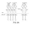
- FIG. 6A illustrates in more detail the output waveguides of an AWG used as a wavelength domain optical demultiplexer (e.g. element 140 of FIG. 1 ) and a digitizer (e.g., element 150 of FIG. 1 ) according to some embodiments.
- 2N photodetectors are respectively coupled to receive light from N sensors.
- the AWG spatially disperses sensor output light having centroid wavelengths ⁇ 1 , ⁇ 2 , ... ⁇ N to the output waveguide pairs 645a,b, 646a,b, ... 647a,b.
- Sensor output light having centroid wavelength ⁇ 1 is dispersed to waveguide pairs 645a, 645b; sensor output light having centroid wavelength ⁇ 2 is dispersed to waveguide pairs 646a, 646b; sensor output light having centroid wavelength ⁇ N is dispersed to waveguide pairs 647a, 647b, etc.
- Light from output waveguide 645a is optically coupled to photodetector 655a which generates signal I 11 in response to the detected light; light from output waveguide 645b is optically coupled to photodetector 655b which generates signal I 12 in response to the detected light; light from output waveguide 646a is optically coupled to photodetector 656a which generates signal I 21 in response to the detected light; light from output waveguide 646b is optically coupled to photodetector 656b which generates signal I 22 in response to the detected light; light from output waveguide 647a is optically coupled to photodetector 657a which generates signal I N1 in response to the detected light; light from output waveguide 647b is optically coupled to photodetector 657b which generates signal I N2 in response to the detected light.
- the AWG causes the spatial position of the sensor's output light to also shift. For example if sensor output light that initially has a centroid at ⁇ 1 shifts to a centroid at ⁇ 1 + ⁇ 1 , as shown in FIG. 6A , the amount of light carried by output waveguide 645a decreases and the amount of light carried by output waveguide 645b increases. Thus, the amount of light detected by photodetector 655a decreases and the amount of light detected by photodetector 655b increases with corresponding changes in the photocurrents I I and I 2 . Thus, a shift in the sensed parameter causes a shift in the sensor output light centroid from ⁇ 1 to ⁇ 1 + A 1 which in turn causes a change in the ratio of I 11 to I 12 .
- the photocurrent of each photodiode may be converted into a voltage with a resistor or transimpedance amplifier, and sensed and digitized.
- the wavelength shift may be calculated for the i th FBG with the following formula: ⁇ i ⁇ ⁇ i ⁇ 0 + ⁇ ⁇ ⁇ 2 ⁇ I 2 ⁇ i - I 2 ⁇ i - 1 I 2 ⁇ i + I 2 ⁇ i - 1
- ⁇ i is the estimated wavelength of the i th FBG
- ⁇ i0 is the center wavelength of an output waveguide pair
- ⁇ is the wavelength spacing between the peak transmission wavelengths of an output waveguide pair
- I 2i and I 2i-1 are the light intensities recorded by the photodetectors at the output of each waveguide in the pair.
- the FBGs have a FWHM roughly equal to ⁇ /2, such that as the reflected peak from the FBG shifts from one photodetector in the pair to the other, there is a continuous and monotonic change in the differential signal of the pair (numerator in the formula above).
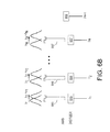
- FIG. 6B illustrates in more detail another configuration of the output waveguides of an AWG used as a wavelength domain optical demultiplexer (e.g. element 140 of FIG. 1 ) and a digitizer (e.g., element 150 of FIG. 1 ) according to some embodiments.
- N photodetectors are respectively coupled to receive light from N sensors.
- the AWG spatially disperses sensor output light having centroid wavelengths ⁇ 1 , ⁇ 2 , ... ⁇ N to the output waveguides 645, 646,... 647.
- Sensor output light having centroid wavelength ⁇ 1 is dispersed to waveguide 645; sensor output light having centroid wavelength ⁇ 2 is dispersed to waveguide 646; sensor output light having centroid wavelength ⁇ N is dispersed to waveguide 647, etc.
- Light from output waveguide 645 is optically coupled to photodetector 655 which generates signal I 1 in response to the detected light;
- light from output waveguide 646 is optically coupled to photodetector 656 which generates signal I 2 in response to the detected light;
- light from output waveguide 647 is optically coupled to photodetector 657 which generates signal I N in response to the detected light.
- the AWG causes the spatial position of the sensor's output light to also shift. For example, if sensor output light that initially has a centroid at ⁇ 1 shifts to a centroid at ⁇ 1 + ⁇ 1 as shown in FIG. 6B , the amount of light carried by output waveguide 645 increases. Thus, the amount of light detected by photodetector 655 increases with a corresponding change in the photocurrent I 1 . Thus, a shift in the sensed parameter causes a shift in the sensor output light centroid from ⁇ 1 to ⁇ 1 + ⁇ 1 , which in turn causes a change in the current I 1 .
- Changes in the photodetector current that are caused by fluctuations of light source intensity can be differentiated from changes in photodetector current caused by wavelength shifts in sensor output light by measuring the light source intensity with an additional photodetector 699 that generates current I N+1 . Then, a wavelength shift can be calculated from the ratio I 1 /I N+1 for sensor 1, I 2 /I N+1 for sensor 2, etc.
- FIG. 7 illustrates in more detail the output waveguides of an AWG used as a wavelength domain optical demultiplexer, an additional dispersive element, and a digitizer according to some embodiments.
- the output light from sensors 1, 2 ... N having initial centroid wavelengths ⁇ 1 , ⁇ 2 , ... ⁇ N is respectively spatially dispersed to output waveguides 745, 746, ... 747 of the AWG.
- the light from output waveguides 745, 746, ... 747 is incident on a linearly variable transmission structure (LVTS) 765, 766, ... 767 or other spatially dispersive optical element.
- LVTS linearly variable transmission structure
- the LVTS includes spreading components 755, 756 ... 757 configured to collimate and/or spread the light from the output waveguide 745, 746 ... 747 across an input surface of LVTS 765, 766, ... 767.
- the LVTS 765, 766, ... 767 comprises a dispersive element, such as a prism or a linear variable filter.
- the LVTS 765, 766, ... 767 receives light at its input surface 765a, 766a, ... 767a from the waveguide 745, 746, ... 747 and (optionally) the spreading component 755, 756,...
- the LVTS 765, 766, ... 767 can serve to further demultiplex the optical signal incident at the input surface 765a, 766a, .... 767a of the LVTS 765, 766,... 767 according to the wavelength of the light.
- Fig. 7 shows two wavelength bands emitted from the LVTS 765, an initial emission band has a centroid wavelength of ⁇ 1 emitted at distance d 1 from a reference position (REF) along the output surface 765b.
- the initial wavelength band shifts to a wavelength band having centroid wavelength ⁇ 1 + ⁇ 1 .
- the shifted wavelength band is emitted at distance d ⁇ 1 from the reference position.
- a photodetector pair 775 is positioned relative to the LVTS 765 so that light transmitted through the LVTS 765 falls on the photodetector pair 775. For example, light having wavelength ⁇ 1 may fall predominantly on photodetector 775a and light having wavelength ⁇ 1 + ⁇ 1 may fall predominantly on photodetector 775b.
- the photodetector 775a generates signal I 11 in response to light falling on its light sensitive surface and photodetector 775b generates signal I 12 in response to light falling on its light sensitive surface.
- the signals I 11 , I 12 include information about the sensed parameter such that a change in the ratio of I 11 and I 12 indicates a change in the sensed parameter, which can be calculated using the equation discussed above.
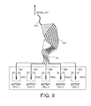
- FIG. 8 shows a portion of a monitoring system including multiple FBG sensors, FBG1, FBG2, FBG3, FBG4, FBG5 respectively disposed on multiple sensor waveguides, 801, 802, 803, 804, 805 inserted in battery cells Battery Cell 1, Battery Cell 2, Battery Cell 3, Battery Cell 4, Battery Cell 5.
- Each of the multiple sensor waveguides is respectively optically connected to an input waveguide 811 of AWG 810.
- the output light from each of the FBG sensors is multiplexed by AWG 810 onto waveguide 812 that may be optically coupled to a circulator and light source (as in 230 of FIG. 2 ) which is then connected to an input waveguide of a wavelength domain demultiplexer, such as AWG 240 shown in FIG. 2 .
- AWGs have been used in high speed communication systems and are designed to minimize crosstalk between adjacent channels. This is important for digital communications because the bit error rate must be made very low (on the order of 10 -12 ) so it is suboptimal for light from one channel to leak into the next.
- Embodiments described herein involve AWGs specifically designed for sensing applications. These AWGs deliberately introduce crosstalk between adjacent channels.
- AWGs with crosstalk are configured so that the center-to-center spacing between adjacent output waveguides in a pair of output waveguides is less than the optical spot size at the output waveguides, where the optical spot size is the full width half maximum (FWHM) of the intensity of the spot.
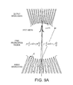
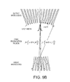
- Fig. 9A the output coupler of an AWG is shown with the spacing of the output waveguides decreased from "normal" telecom operation to introduce crosstalk between adjacent channels.
- the spacing of the array waveguides is d, and the change in position of the optical spot at the input of the output waveguides for a change in wavelength ⁇ ⁇ is given as: ⁇ ⁇ x ⁇ m ⁇ f ⁇ ⁇ ⁇ ⁇ / d , where f is the distance from the array waveguides to the output waveguides (note the radius of curvature of both the input and output side of the slab waveguide is also f , so that the optical spot comes to a focus at the output waveguides).
- the spacing of a pair of output waveguides should represent a translation of the spot from mostly on one waveguide to mostly on the other waveguide as the FBG's reflected wavelength translates over its range. That is, for a change in reflected center wavelength ⁇ ⁇ , the spacing of the pair should be chosen according to the formula above. However, the center wavelength of different pairs of output waveguides should be tailored so as to not cause interference between the different pairs (for example, if 8 channels are equally spaced in an AWG, using channels 1 and 2 for the first sensor, 4 and 5 for the second sensor, and 7 and 8 for the third sensor would provide adequate isolation between the sensor readouts in some circumstances).
- the optical spot size at a pair of output waveguides is on the order of the lateral translation of the spot expected over the range of operation of the sensor, which should in turn be on the order of the pair spacing. If the spot is too broad compared to the spacing, the differential signal between the two output waveguides within the pair will be small, and if it is too narrow, the dynamic range of the sensor will be limited.
- the spot size can be estimated from diffraction considerations to be roughly 2 f ⁇ / Kd, where K is the number of array waveguides and ⁇ is the operating wavelength.
- the channel spacing/spot size ratio is adjusted by keeping the spot size fixed (assuming it is already the proper size for operation, e.g., to provide optimal operation), but decreasing the output waveguide spacing.
- the channel spacing is assumed to be sufficient, e.g., optimal, according to the above considerations, but the spot size is increased to be within its optimal range by decreasing the number of array waveguides K.
- adjusting the spot size relative to the channel spacing may be implemented by moving the output waveguides away from the focal length f 0 of the array waveguides to a new distance f, such that the spot size becomes roughly Kd
- decreasing the number of sources broadens the angular distribution of the light emanating from an array of coherent sources.
- This phenomenon can be understood in analogy to a smaller lens having poorer diffraction-limited performance compared to a bigger lens. Therefore, even a relatively narrow spectral peak can be distributed across two channels so that an intensity-independent wavelength shift can be detected.
- optical time domain multiplexing is used in conjunction with the previously described optical wavelength division multiplexing and demultiplexing. For each input of a multi-input AWG, there is a known wavelength-dependent mapping to the output waveguides. Therefore, time division multiplexing and wavelength division demultiplexing can be combined to address a far greater number of sensors than could be addressed with either method alone.
- the optical switches could be integrated onto the same substrate as the AWG allowing fabrication of modules having an identical structure.
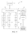
- FIG. 11 shows a block diagram of a monitoring system 1100 that is similar in some respects to the monitoring system 100 of FIG. 1 and where like reference numbers indicate similar elements.
- System 1100 is capable of monitoring M modules 1121, 1122, ... 1123, each module having N sensors.
- the optical outputs of the N sensors of each module 1121, 1122, ... 1123 may be carried on a single optical fiber 1131, 1132, 1133 where the optical outputs of the sensors are distributed in wavelength according to the output channels of the optical demultiplexer.
- the modules and the optical fibers/sensors may be identically constructed.
- Input light is passed from the light source 110 to the modules 1121, 1122, ... 1123 through optical time domain mux 1170 and through waveguides 1131, 1132, ... 1133, and interacts with the sensors S11 ... SNM.
- Output light from the modules 1121, 1122, ... 1123 is passed to the optical wavelength domain demultiplexer 140 through the optical time domain multiplexer 1170.
- the modules 1121, 1122, ... 1123 are selected one at a time by the optical time domain multiplexer 1170.
- Implementations that combine time domain multiplexing and wavelength domain multiplexing and demultiplexing of sensor output light as disclosed herein are able to address a far greater number of battery cells (or other energy system components) than could be addressed by either time domain multiplexing or wavelength domain multiplexing/demultiplexing alone.
- FIG. 12 shows a configuration of a system 1200 that uses both time domain multiplexing and wavelength domain multiplexing to address multiple modules having multiple FBG sensors.
- the system 1200 monitors a battery pack using M sensor modules, each module having N FBG sensors S1, S2, ... SN disposed in battery cells on a single optical fiber.
- the N FBGs are distributed in wavelength according to the output channels of an AWG 1240 used as an optical wavelength domain demultiplexer.
- the modules and the optical fibers/FBGs may be all identically constructed.
- Light is passed from the light source 110 to the battery modules by way of a 1 x M optical power splitter 1201 and M circulators 1270. Sensor output light from Modules 1, 2, ...
- the time domain multiplexer 1250 comprises a bank of M optical switches controlled by switch control circuitry 1280.
- the output waveguides 1231, 1232, ... 1233 of the modules 1 to M are selected one at a time and are optically coupled to the respective input waveguide of the AWG 1240.
- the AWG 1240 spatially disperses the light from the sensor modules to the AWG output waveguides 1241 and then the output light is routed to digitizer 1260 as previously discussed.
- FIG. 12 depicts sensors S1, S2, ... SN arranged so that the output light of each sensor is multiplexed onto the single output waveguide 1231, 1232, ... 1233 for the module.
- FIG. 13 shows an alternative configuration for multiplexing sensor output light having different wavelength bands at the module level.
- each battery cell 1301 is monitored by one or more FBGs 1302 disposed on a sensor optical waveguide 1303.
- Input light is optically coupled through a 1 x N power splitter 1371 to circulators 1370.
- the circulators 1370 connect the sensor output waveguides 1303 in parallel to through an N x 1 power splitter 1372 to the output waveguide 1320 for the module 1305.
- the output waveguide carries the combined (wavelength multiplexed) output light from all FBGs 1302 in the module 1305.
- the module arrangement shown in FIG. 13 can be used to replace each of the modules shown in FIGS. 8 or 12 , for example.
- FIG. 14 depicts another monitoring system 1400 that uses time domain multiplexing and wavelength domain multiplexing in accordance with some implementations.
- the monitoring system 1400 of FIG. 14 is similar in some respects to the monitoring system of 1200 and like reference numbers are used to refer to similar elements.
- System 1400 replaces the M optical switches 1250 and M optical circulators 1270 with a 1 X M optical switch 1450 and an optical circulator 1470 disposed between the switch 1450 and light source 110.
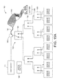
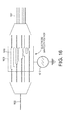
- FIG. 15A illustrates a monitoring system 1500 that includes a hierarchical switching arrangement to implement optical time domain multiplexing.
- the switching arrangement 1550 in the illustrated monitoring system 1500 includes a first level of four 1 x 2 optical switches 1551 (the bottom-most level of switches in FIG. 15A ) coupled to 8 sensor modules, a second level of two 1 x 2 optical switches 1552 (the next to bottom-most level of switches in FIG. 15A ) optically coupled between the first level switches 1551 and a single 1 x 2 third level optical switch 1553.
- the switching arrangement 1550 is connected to the light source 110 and the wavelength division demultiplexer (AWG) 1540 through an optical circulator 1570.
- AMG wavelength division demultiplexer
- the switches 1551, 1552, 1553 are controlled by switch control circuitry 1580 such that the output light from each sensor module is time multiplexed into the input waveguide 1541 of the AWG.
- the AWG 1540 demultiplexes the time multiplexed sensor output light, spatially dispersing the output light according to wavelength to the output waveguides and to the digitizer 1560.
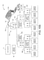
- FIG. 15B illustrates a monitoring system 1501 that includes a hierarchical switching arrangement with integrated switch control to implement optical time division multiplexing.
- the switching arrangement 1590 in the illustrated monitoring system 1501 includes a first (bottom-most) level of four 1 x 2 optical switches 1591 coupled to 8 sensor modules, a second (next highest) level of two 1 x 2 optical switches 1592 optically coupled between the first level switches 1591 and the single 1 x 2 third level optical switch 1593.
- the switching arrangement 1590 is connected to the light source 110 and the wavelength division demultiplexer (AWG) 1540 through an optical circulator 1570.
- AMG wavelength division demultiplexer
- the switches 1591, 1592, 1593 are controlled by integrated switch control circuitry 1582 and optionally additionally by central switch control circuitry 1581 such that the output light from each sensor module is time multiplexed into the input waveguide 1541 of the AWG.
- the AWG 1540 demultiplexes the time multiplexed sensor output light, spatially dispersing the output light according to wavelength to the output waveguides and to the digitizer 1560.
- the switch control circuitry 1581, 1582 operates to time multiplex output light from the sensor modules to the AWG 1540.
- at least one of the switches 1591, 1592, 1593 or groups of switches are associated with an integrated switch control element 1582.
- a control signal to change switch state is carried to an integrated switch control element 1582 from other integrated switch control elements or from the central switch control 1581 by the optical waveguides 1583 that optically couple the switches 1591, 1592, 1593.
- the integrated switch control may include electro-optical components or circuitry configured to receive an optical control signal, e.g., a digital signal, that includes a command to change switch state via the waveguide; to interpret the command; and to control the switch to change switch state.
- switch control to implement time division multiplexing may be performed by the integrated switch control elements in communication with each other.
- the integrated switch control elements have the capability of receiving and interpreting commands to change switch state as well as sending commands to other integrated switch control elements.
- the switch control may be implemented by the integrated switch control elements operating in conjunction with a central switch control.
- optical switches can be used for the time division multiplexers discussed herein.
- Suitable optical switch technologies include micro-electro-mechanical systems (MEMS) optical switches, liquid crystal switches, bubble switches, thermo-optic switches, phased-array switches, and electro-holographic switches, for example.
- MEMS micro-electro-mechanical systems
- the optical time division multiplexer may be implemented by a 1 x M phased array optical switch as illustrated in FIG. 16 .
- the input optical signals carried on input waveguides 1601 are time multiplexed to an output waveguide 1602 by a voltage-controlled phase modulator section 1603 having a phase delay material 1605, such as LiNbO 3 , of varying length along the input waveguides 1601.
- the voltage controlled phase modulator 1603 can be configured to induce phase modulation along the input waveguides 1601 in response to a time varying electrical signal 1610, such as the sawtooth wave shown.
- the phase modulator material 1605 may have a linearly varying length along the input waveguides 1601 to provide a linearly varying phase modulation such that time multiplexing can be implemented by a linearly varying periodic electrical signal 1610.
- Other configurations for the phase delay switch are possible, including different waveforms, separate electrodes for each waveguide within the phase modulator section, identical length phase shifting sections, other phase shifting waveforms, silicon phase modulators based on free-carrier injection, etc.
- the monitoring systems proposed herein may include one or more components that are integrated onto the same substrate.
- the photodetectors e.g., photodiodes
- the photodetectors could be integrated directly into the output waveguides of the AWG. Integrating one or more of the monitoring system components onto the same substrate can yield substantial cost, size, and complexity savings. Note that it may be possible to integrate all components onto the same substrate, including the light source, circulator, optical switches, AWG, photodiodes, and digitizer, using electronic/photonic circuit hybrid integration methods.
- the approaches discussed herein can provide a high degree of sensor multiplexing with a single detector portion as well as the potential for high levels of integration.
- Some or all components of the detector portion of the monitoring system - light source, circulator(s), time division multiplexer, wavelength division demultiplexer, and digitizer - could be integrated onto the same substrate, with the only external connections being electrical connections to a power source, electrical and/or optical communications with the monitoring and/or management processor, and optical fiber connections to the sensors.
- Such an integrated device could potentially yield significant cost/size/performance enhancements when manufactured in high volumes (e.g., automotive) as compared to non-integrated approaches.
- the proposed combination of time and wavelength-domain multiplexing for modular battery packs can enable pack monitoring with a compact, centralized readout.
- a single fiber-optic cable can be used for each module, reducing cost and cabling.
- the wavelength coupling to the various output channels can be selected for sensing applications by deliberately introduced/designed cross-talk between adjacent channels.
- the single centralized readout can also be used to read out other optical fiber sensors distributed across the vehicle, especially in combination with the hierarchical network of time-domain multiplexers.
- Different waveguide materials for the AWG would be used depending on the wavelengths of the optical sensors. For example, although silicon can be used at telecommunications wavelengths (around 1550 nm) it is not suitable for use in the visible wavelength range, which may be of more interest for chemical sensing approaches. In the visible wavelength range, silicon dioxide may be suitable as a waveguide material; in addition, silicon dioxide is also transparent at telecommunications wavelengths.
- all 2N outputs of the AWG may be measured.
- An estimation routine may be employed using that information to simultaneously determine the centroids and peak intensities of up to N spectral peaks with known shape. For example, all spectral peaks may be fit simultaneously to all of the recorded information.
- time domain multiplexing and wavelength domain multiplexing/demultiplexing can be employed, with reduction in the overall cost and/or size and/or complexity of the entire system being a goal in some implementations.
- Other schemes for time multiplexing using multiple light sources fired sequentially in time can also potentially be employed.
- light source A covering a spectral range A and light source B covering a substantially different spectral range B can be coupled onto the same optical fiber.
- Sensors can be placed along the fiber such that a portion of the sensors produce a response when excited in the spectral range A and another portion of the sensors produce a response when excited in the spectral range B.
- the AWG channel wavelengths can be tuned in situ with a temperature controller, or athermalized AWGs (where the dependence on temperature of the channel center wavelengths has been reduced or minimized) can be used. It may still be useful to incorporate some facility to measure the temperature of the AWG and to include that information in any algorithm which calculates a wavelength shift from photodiode currents. In implementations that measure a wavelength shift from looking at the difference in light flux at the output of a pair of adjacent AWG waveguides, there is a tradeoff between the dynamic range with which the wavelength shift of a single spectral peak can be measured and the number of peaks that can be measured with a single AWG.
- each peak can be measured with the same resolution as before, but it can also be measured with 10x the range.
- the AWG may be used for presorting of the different spectral peaks, and the wavelength shift of each spectral peak is then determined using a linearly varying transmission structure and photodetector array as described above.
- Systems, devices, or methods disclosed herein may include one or more of the features, structures, methods, or combinations thereof described herein.
- a device or method may be implemented to include one or more of the features and/or processes described herein. It is intended that such device or method need not include all of the features and/or processes described herein, but may be implemented to include selected features and/or processes that provide useful structures and/or functionality.
Landscapes
- Physics & Mathematics (AREA)
- General Physics & Mathematics (AREA)
- Optics & Photonics (AREA)
- Engineering & Computer Science (AREA)
- Microelectronics & Electronic Packaging (AREA)
- Investigating Or Analysing Materials By Optical Means (AREA)
- Spectroscopy & Molecular Physics (AREA)
- Secondary Cells (AREA)
- Optical Modulation, Optical Deflection, Nonlinear Optics, Optical Demodulation, Optical Logic Elements (AREA)
- Theoretical Computer Science (AREA)
- Mathematical Physics (AREA)
- Health & Medical Sciences (AREA)
- Life Sciences & Earth Sciences (AREA)
- Chemical & Material Sciences (AREA)
- Analytical Chemistry (AREA)
- Biochemistry (AREA)
- General Health & Medical Sciences (AREA)
- Immunology (AREA)
- Pathology (AREA)
- Optical Transform (AREA)
Applications Claiming Priority (1)
| Application Number | Priority Date | Filing Date | Title |
|---|---|---|---|
| US14/331,318 US9677916B2 (en) | 2014-07-15 | 2014-07-15 | Energy system monitoring |
Publications (2)
| Publication Number | Publication Date |
|---|---|
| EP2975366A1 true EP2975366A1 (de) | 2016-01-20 |
| EP2975366B1 EP2975366B1 (de) | 2018-01-31 |
Family
ID=53525079
Family Applications (1)
| Application Number | Title | Priority Date | Filing Date |
|---|---|---|---|
| EP15174916.5A Active EP2975366B1 (de) | 2014-07-15 | 2015-07-01 | Energiesystemüberwachung |
Country Status (4)
| Country | Link |
|---|---|
| US (1) | US9677916B2 (de) |
| EP (1) | EP2975366B1 (de) |
| JP (1) | JP6491970B2 (de) |
| KR (1) | KR102221911B1 (de) |
Cited By (10)
| Publication number | Priority date | Publication date | Assignee | Title |
|---|---|---|---|---|
| CN107748337A (zh) * | 2017-11-09 | 2018-03-02 | 常州格力博有限公司 | 多电池串联检测电路 |
| EP3425361A1 (de) * | 2017-07-06 | 2019-01-09 | Palo Alto Research Center Incorporated | Optische überwachung für stromnetzsysteme |
| EP3543658A1 (de) * | 2018-03-23 | 2019-09-25 | Saab Ab | System und verfahren zur bestimmung von temperaturänderungen einer optischen faser |
| EP4075101A1 (de) * | 2021-04-16 | 2022-10-19 | Viavi Solutions Inc. | Datensammlung und analyse-basierte vorrichtungsüberwachung |
| US20230050697A1 (en) * | 2020-01-30 | 2023-02-16 | Safran | System for measuring a plurality of physical parameters at a measurement point with a multimode optical fiber |
| US11585692B2 (en) | 2019-10-24 | 2023-02-21 | Palo Alto Research Center Incorporated | Fiber optic sensing system for grid-based assets |
| US11719559B2 (en) | 2019-10-24 | 2023-08-08 | Palo Alto Research Center Incorporated | Fiber optic sensing system for grid-based assets |
| US12031859B2 (en) | 2021-04-16 | 2024-07-09 | Viavi Solutions Inc. | Optical fiber-based sensing membrane |
| IT202400003457A1 (it) | 2024-02-19 | 2025-08-19 | Vincenzo Romano Marrazzo | Sistema multicanale per misure compensate di sensori in fibra ottica completamente analogico |
| US12576748B2 (en) | 2021-04-16 | 2026-03-17 | Viavi Solutions Inc. | Data collection and analysis-based device monitoring |
Families Citing this family (19)
| Publication number | Priority date | Publication date | Assignee | Title |
|---|---|---|---|---|
| US10403922B2 (en) | 2014-07-23 | 2019-09-03 | Palo Alto Research Center Incorporated | Battery with embedded fiber optic cable |
| US10446886B2 (en) | 2014-07-23 | 2019-10-15 | Palo Alto Research Center Incorporated | Embedded fiber optic cables for battery management |
| EP3384248B1 (de) * | 2015-12-02 | 2021-03-10 | Danmarks Tekniske Universitet | Optische messvorrichtung mit einem interrogator und einem monomodem polymerbasierten faseroptischen sensorsystem |
| US10050316B2 (en) * | 2016-05-13 | 2018-08-14 | Infineon Technologies Ag | Communication between battery cells |
| US10106049B2 (en) * | 2016-05-18 | 2018-10-23 | Nxp Usa, Inc. | Battery monitoring device |
| US10574365B2 (en) * | 2016-10-14 | 2020-02-25 | Tiveni Mergeco, Inc. | Optical communications interface for battery modules of an energy storage system |
| US10234633B2 (en) * | 2017-03-03 | 2019-03-19 | Nec Corporation | Transmitter/receiver with orbital angular momentum based optical encryption |
| US10317256B2 (en) | 2017-04-14 | 2019-06-11 | Palo Alto Research Center Incorporated | Monitoring transportation systems |
| JP7075747B2 (ja) * | 2017-12-06 | 2022-05-26 | Nttエレクトロニクス株式会社 | 光波長合分波器 |
| EP3517938B1 (de) | 2018-01-30 | 2020-09-16 | Karlsruher Institut für Technologie | Optischer detektor und verfahren zum nachweis einer chemischen verbindung |
| US11276891B2 (en) | 2019-08-20 | 2022-03-15 | Kidde Technologies, Inc. | Lithium ion battery protection system |
| US11476631B2 (en) * | 2019-11-24 | 2022-10-18 | Nokia Solutions And Networks Oy | Photonic chip integrated with a fiber laser |
| US11051089B1 (en) * | 2020-03-27 | 2021-06-29 | The Boeing Company | Microwave photonics enabled beam-forming and channelization |
| JP7484615B2 (ja) * | 2020-09-24 | 2024-05-16 | マツダ株式会社 | 車両用電池の状態検出方法及び検出制御装置 |
| US11163105B1 (en) | 2020-12-28 | 2021-11-02 | Palo Alto Research Center Incorporated | System for optical sensing |
| US12085768B2 (en) * | 2021-09-02 | 2024-09-10 | Advanced Semiconductor Engineering, Inc. | Optical module |
| US11733468B2 (en) | 2021-12-08 | 2023-08-22 | Viavi Solutions Inc. | Photonic structure using optical heater |
| JP7634040B2 (ja) * | 2022-05-13 | 2025-02-20 | キストラー ホールディング アクチエンゲゼルシャフト | 光学的に動作する温度センサ、当該温度センサの使用法、及び少なくとも1つの温度センサを備える電池セル組立体 |
| CN121142315B (zh) * | 2025-09-01 | 2026-04-07 | 西安电子科技大学 | 一种紧凑型多通道电池组监测集成电路 |
Citations (4)
| Publication number | Priority date | Publication date | Assignee | Title |
|---|---|---|---|---|
| US20040033004A1 (en) * | 2001-10-09 | 2004-02-19 | Welch David F. | Optical signal receiver photonic integrated circuit (RxPIC), an associated optical signal transmitter photonic integrated circuit (TxPIC) and an optical network transmission system utilizing these circuits |
| US20060045412A1 (en) * | 2004-09-02 | 2006-03-02 | National Research Council Of Canada | Simultaneous interrogation of multi wavelength-modulated fiber optical sensors by modulating an arrayed waveguide grating based demultiplexer |
| US20120321242A1 (en) * | 2010-01-25 | 2012-12-20 | Wolfgang Schade | Sensor element and method for the production thereof and use thereof |
| US20140092375A1 (en) * | 2012-09-28 | 2014-04-03 | Palo Alto Research Center Incorporated | Monitoring and management for energy storage devices |
Family Cites Families (61)
| Publication number | Priority date | Publication date | Assignee | Title |
|---|---|---|---|---|
| US4240747A (en) | 1979-10-03 | 1980-12-23 | Battelle Memorial Institute | Refractive-index responsive light-signal system |
| JPS63301470A (ja) | 1987-05-30 | 1988-12-08 | Tomoo Matsuo | バッテリ充電システム |
| DE4411289A1 (de) | 1994-03-31 | 1995-10-05 | Varta Batterie | Mehrzellige Akkumulatorenbatterie |
| US5995686A (en) | 1997-12-16 | 1999-11-30 | Hamburger; Robert N. | Fiber-optic sensor device and method |
| US6265100B1 (en) | 1998-02-23 | 2001-07-24 | Research International, Inc. | Rechargeable battery |
| US6051437A (en) | 1998-05-04 | 2000-04-18 | American Research Corporation Of Virginia | Optical chemical sensor based on multilayer self-assembled thin film sensors for aquaculture process control |
| US5949219A (en) | 1998-07-24 | 1999-09-07 | The United States Of America As Represented By The United States Department Of Energy | Optical state-of-charge monitor for batteries |
| JP3397699B2 (ja) * | 1998-08-26 | 2003-04-21 | 日本電信電話株式会社 | 時間分割型波長監視装置 |
| US6285807B1 (en) | 1998-11-16 | 2001-09-04 | Trustees Of Tufts College | Fiber optic sensor for long-term analyte measurements in fluids |
| US7306951B1 (en) | 1999-06-08 | 2007-12-11 | Midwest Research Institute | Method and apparatus for determining diffusible hydrogen concentrations |
| US6379969B1 (en) | 2000-03-02 | 2002-04-30 | Agilent Technologies, Inc. | Optical sensor for sensing multiple analytes |
| CA2445127C (en) | 2001-05-04 | 2011-12-13 | Sensors For Medicine And Science, Inc. | Electro-optical sensing device with reference channel |
| US6828055B2 (en) | 2001-07-27 | 2004-12-07 | Hewlett-Packard Development Company, L.P. | Bipolar plates and end plates for fuel cells and methods for making the same |
| EP1436931B1 (de) * | 2001-10-09 | 2005-12-28 | Infinera Corporation | Digitale optische netzwerkarchitektur |
| EP1324516B1 (de) * | 2001-12-21 | 2005-12-14 | Agilent Technologies, Inc. (a Delaware corporation) | Verfahren und Gerät zur Detektierung von Übersprechen |
| US20050026134A1 (en) | 2002-04-10 | 2005-02-03 | Bioprocessors Corp. | Systems and methods for control of pH and other reactor environment conditions |
| WO2005043632A1 (en) | 2003-11-03 | 2005-05-12 | Sustainable Technologies International Pty Ltd | Multilayered photovoltaic device on envelope surface |
| US7642742B2 (en) | 2003-12-01 | 2010-01-05 | Societe Bic | Fuel cell system with fuel supply monitoring system and method of use |
| US7155075B2 (en) | 2004-03-29 | 2006-12-26 | General Electric Company | Optical battery temperature monitoring system and method |
| US7310153B2 (en) | 2004-08-23 | 2007-12-18 | Palo Alto Research Center, Incorporated | Using position-sensitive detectors for wavelength determination |
| US7522786B2 (en) | 2005-12-22 | 2009-04-21 | Palo Alto Research Center Incorporated | Transmitting light with photon energy information |
| US8980453B2 (en) | 2008-04-30 | 2015-03-17 | Medtronic, Inc. | Formation process for lithium-ion batteries |
| US7511823B2 (en) | 2004-12-21 | 2009-03-31 | Halliburton Energy Services, Inc. | Fiber optic sensor |
| US7695970B2 (en) | 2005-03-04 | 2010-04-13 | University Of Connecticut | Optical fiber based fluorescence sensor for in-situ measurement and control of fuel cells |
| JP4694278B2 (ja) | 2005-04-28 | 2011-06-08 | 本田技研工業株式会社 | バッテリユニット構造 |
| US7433552B2 (en) | 2005-12-22 | 2008-10-07 | Palo Alto Research Center Incorporated | Obtaining analyte information |
| US7315667B2 (en) | 2005-12-22 | 2008-01-01 | Palo Alto Research Center Incorporated | Propagating light to be sensed |
| US8437582B2 (en) | 2005-12-22 | 2013-05-07 | Palo Alto Research Center Incorporated | Transmitting light with lateral variation |
| US7263246B1 (en) | 2006-02-21 | 2007-08-28 | United States Of America Department Of Energy | Oxygen detection using evanescent fields |
| US8268493B2 (en) | 2006-05-30 | 2012-09-18 | University Of Connecticut | Fiber optic based in-situ diagnostics for PEM fuel cells |
| US7718948B2 (en) | 2006-12-04 | 2010-05-18 | Palo Alto Research Center Incorporated | Monitoring light pulses |
| JP4930034B2 (ja) | 2006-12-15 | 2012-05-09 | 日立電線株式会社 | 物理量測定システム |
| US7787726B2 (en) * | 2007-03-14 | 2010-08-31 | General Electric Company | Temperature sensing fabric |
| US8143070B2 (en) | 2007-06-05 | 2012-03-27 | Ecolab Usa Inc. | Optical cell |
| CN101119036B (zh) | 2007-07-23 | 2011-01-19 | 柏禄帕迅能源科技有限公司 | 用于电动汽车的电池管理系统 |
| JP2009059582A (ja) | 2007-08-31 | 2009-03-19 | Toyota Motor Corp | 二次電池の圧力検出装置 |
| US8049894B2 (en) * | 2007-10-05 | 2011-11-01 | Lightwaves 2020, Inc. | Multiple wavelength optical analyzer device |
| JP5229806B2 (ja) | 2008-01-25 | 2013-07-03 | 独立行政法人海洋研究開発機構 | 水中における二酸化炭素濃度の測定装置及び方法 |
| US8241911B2 (en) | 2008-11-07 | 2012-08-14 | Mocon, Inc. | Calibration card for photoluminescent oxygen sensors with zero point maintained with a metal-air battery |
| US8019190B2 (en) | 2009-03-30 | 2011-09-13 | General Electric Company | Optical sensors, systems, and methods of making |
| JP2010281760A (ja) * | 2009-06-08 | 2010-12-16 | Aisan Ind Co Ltd | 物理量測定装置 |
| DE102009029002B3 (de) * | 2009-08-28 | 2011-01-27 | Fraunhofer-Gesellschaft zur Förderung der angewandten Forschung e.V. | Photoakustischer Sensor sowie Verfahren zu seiner Herstellung und Verwendung |
| JP4580037B1 (ja) | 2010-03-29 | 2010-11-10 | エンパイア テクノロジー ディベロップメント エルエルシー | 電池システム、及び電池の安全警報システム |
| JP4580038B1 (ja) | 2010-04-27 | 2010-11-10 | エンパイア テクノロジー ディベロップメント エルエルシー | 電池システム、及び電池の安全警報システム |
| US8729862B2 (en) | 2010-12-17 | 2014-05-20 | Lenovo (Singapore) Pte. Ltd. | Controlled regeneration of solid electrolyte interface for prolonged cycling of lithium batteries |
| KR101217074B1 (ko) | 2011-02-21 | 2012-12-31 | 로베르트 보쉬 게엠베하 | 배터리 관리 시스템 |
| US20120219847A1 (en) | 2011-02-24 | 2012-08-30 | Samsung Sdi Co., Ltd. | Pouch type battery and its manufacturing method |
| US9693716B2 (en) | 2011-03-09 | 2017-07-04 | Medtronic, Inc. | Optical sensor system and measurement method |
| SG193922A1 (en) | 2011-04-05 | 2013-11-29 | Blacklight Power Inc | H2o-based electrochemical hydrogen-catalyst power system |
| US9401247B2 (en) | 2011-09-21 | 2016-07-26 | Semiconductor Energy Laboratory Co., Ltd. | Negative electrode for power storage device and power storage device |
| JP5826645B2 (ja) * | 2012-01-23 | 2015-12-02 | 株式会社豊田自動織機 | 温度センサ用光ファイバおよび電力装置監視システム |
| US9490507B2 (en) | 2012-05-22 | 2016-11-08 | Lawrence Livermore National Security, Llc | Li-ion battery thermal runaway suppression system using microchannel coolers and refrigerant injections |
| US9267993B2 (en) | 2012-05-23 | 2016-02-23 | Lawrence Livermore National Security, Llc | Battery management system with distributed wireless sensors |
| US9704384B2 (en) | 2012-05-22 | 2017-07-11 | Lawrence Livermore National Security, Llc | Battery management systems with thermally integrated fire suppression |
| JP2015535334A (ja) | 2012-08-10 | 2015-12-10 | バテル・メモリアル・インスティテュートBattelle Memorial Institute | バッテリ健全性の光学的モニタリング |
| US9209494B2 (en) | 2012-09-28 | 2015-12-08 | Palo Alto Research Center Incorporated | Monitoring/managing electrochemical energy device using detected intercalation stage changes |
| US9865895B2 (en) | 2013-03-12 | 2018-01-09 | Ess Tech, Inc. | Methods to prepare stable electrolytes for iron redox flow batteries |
| WO2014145756A1 (en) | 2013-03-15 | 2014-09-18 | Design Flux Technologies, Llc | Method and apparatus for creating a dynamically reconfigurable energy storage device |
| US10230125B2 (en) | 2014-03-06 | 2019-03-12 | Ess Tech, Inc. | Method and system to maintain electrolyte stability for all-iron redox flow batteries |
| US9509011B2 (en) | 2013-06-07 | 2016-11-29 | Ess Tech, Inc. | Method and system for rebalancing electrolytes in a redox flow battery system |
| US10063066B2 (en) | 2014-01-07 | 2018-08-28 | Utah State University | Battery control |
-
2014
- 2014-07-15 US US14/331,318 patent/US9677916B2/en active Active
-
2015
- 2015-07-01 JP JP2015132336A patent/JP6491970B2/ja active Active
- 2015-07-01 KR KR1020150093867A patent/KR102221911B1/ko active Active
- 2015-07-01 EP EP15174916.5A patent/EP2975366B1/de active Active
Patent Citations (4)
| Publication number | Priority date | Publication date | Assignee | Title |
|---|---|---|---|---|
| US20040033004A1 (en) * | 2001-10-09 | 2004-02-19 | Welch David F. | Optical signal receiver photonic integrated circuit (RxPIC), an associated optical signal transmitter photonic integrated circuit (TxPIC) and an optical network transmission system utilizing these circuits |
| US20060045412A1 (en) * | 2004-09-02 | 2006-03-02 | National Research Council Of Canada | Simultaneous interrogation of multi wavelength-modulated fiber optical sensors by modulating an arrayed waveguide grating based demultiplexer |
| US20120321242A1 (en) * | 2010-01-25 | 2012-12-20 | Wolfgang Schade | Sensor element and method for the production thereof and use thereof |
| US20140092375A1 (en) * | 2012-09-28 | 2014-04-03 | Palo Alto Research Center Incorporated | Monitoring and management for energy storage devices |
Cited By (20)
| Publication number | Priority date | Publication date | Assignee | Title |
|---|---|---|---|---|
| EP3425361A1 (de) * | 2017-07-06 | 2019-01-09 | Palo Alto Research Center Incorporated | Optische überwachung für stromnetzsysteme |
| US11860242B2 (en) | 2017-07-06 | 2024-01-02 | Xerox Corporation | Optical monitoring for power grid systems |
| CN107748337A (zh) * | 2017-11-09 | 2018-03-02 | 常州格力博有限公司 | 多电池串联检测电路 |
| EP4063800A1 (de) * | 2018-03-23 | 2022-09-28 | Saab Ab | System und verfahren zur bestimmung von dehnungsänderungen einer optischen faser |
| EP3543658A1 (de) * | 2018-03-23 | 2019-09-25 | Saab Ab | System und verfahren zur bestimmung von temperaturänderungen einer optischen faser |
| US11248969B2 (en) | 2018-03-23 | 2022-02-15 | Saab Ab | System and method for determining temperature changes of an optical fibre |
| US12241794B2 (en) | 2018-03-23 | 2025-03-04 | Saab Ab | System and method for determining changes of an optical fibre |
| US12031871B2 (en) | 2018-03-23 | 2024-07-09 | Saab Ab | System and method for determining changes of an optical fibre |
| EP4043835A1 (de) * | 2018-03-23 | 2022-08-17 | Saab Ab | System und verfahren zur bestimmung von druckänderungen einer optischen faser |
| US11585692B2 (en) | 2019-10-24 | 2023-02-21 | Palo Alto Research Center Incorporated | Fiber optic sensing system for grid-based assets |
| US11719559B2 (en) | 2019-10-24 | 2023-08-08 | Palo Alto Research Center Incorporated | Fiber optic sensing system for grid-based assets |
| US20230050697A1 (en) * | 2020-01-30 | 2023-02-16 | Safran | System for measuring a plurality of physical parameters at a measurement point with a multimode optical fiber |
| US12313433B2 (en) * | 2020-01-30 | 2025-05-27 | Safran | System for measuring a plurality of physical parameters at a measurement point with a multimode optical fiber |
| US12031859B2 (en) | 2021-04-16 | 2024-07-09 | Viavi Solutions Inc. | Optical fiber-based sensing membrane |
| US12092515B2 (en) | 2021-04-16 | 2024-09-17 | Viavi Solutions Inc. | Optical fiber-based sensing membrane layout |
| EP4075101A1 (de) * | 2021-04-16 | 2022-10-19 | Viavi Solutions Inc. | Datensammlung und analyse-basierte vorrichtungsüberwachung |
| US12281934B2 (en) | 2021-04-16 | 2025-04-22 | Viavi Solutions Inc. | Optical fiber-based sensing membrane layout |
| US12474202B2 (en) | 2021-04-16 | 2025-11-18 | Viavi Solutions Inc. | Optical fiber-based sensing membrane |
| US12576748B2 (en) | 2021-04-16 | 2026-03-17 | Viavi Solutions Inc. | Data collection and analysis-based device monitoring |
| IT202400003457A1 (it) | 2024-02-19 | 2025-08-19 | Vincenzo Romano Marrazzo | Sistema multicanale per misure compensate di sensori in fibra ottica completamente analogico |
Also Published As
| Publication number | Publication date |
|---|---|
| KR102221911B1 (ko) | 2021-03-04 |
| US20160018319A1 (en) | 2016-01-21 |
| JP6491970B2 (ja) | 2019-03-27 |
| KR20160008962A (ko) | 2016-01-25 |
| US9677916B2 (en) | 2017-06-13 |
| JP2016020900A (ja) | 2016-02-04 |
| EP2975366B1 (de) | 2018-01-31 |
Similar Documents
| Publication | Publication Date | Title |
|---|---|---|
| EP2975366B1 (de) | Energiesystemüberwachung | |
| US11860242B2 (en) | Optical monitoring for power grid systems | |
| US20240044676A1 (en) | Distributed Optical Fibre Vibration Sensor | |
| Gholamzadeh et al. | Fiber optic sensors | |
| Kersey et al. | Fiber grating sensors | |
| Werneck et al. | A guide to fiber Bragg grating sensors | |
| US7283692B2 (en) | Simultaneous interrogation of multi wavelength-modulated fiber optical sensors by modulating an arrayed waveguide grating based demultiplexer | |
| CN101852626A (zh) | 窄带分布反馈激光器波长扫描光纤光栅传感装置 | |
| US6879742B2 (en) | Using intensity and wavelength division multiplexing for fiber Bragg grating sensor system | |
| Zhuang et al. | On-chip sub-picometer continuous wavelength fiber-Bragg-grating interrogator | |
| Cusano et al. | Multifunction fiber optic sensing system for smart applications | |
| Fusiek et al. | Temperature-independent high-speed distributed voltage measurement using intensiometric FBG interrogation | |
| CN108267160A (zh) | 时分复用的光纤布拉格光栅传感系统 | |
| US20250007604A1 (en) | Optical time domain reflectometer (otdr)-based fiber monitoring optimization | |
| Henderson | Highly-multiplexed grating-sensors for temperature-referenced quasi-static measurements of strain in concrete bridges | |
| Xiao et al. | Arrayed-waveguide-grating-based interrogator for wavelength-modulated multi-fiber-optic sensor applications | |
| Nishiyama et al. | Optical intensity-based measurement of multipoint hetero-core fiber sensors by the method of time-differentiation in optical loss | |
| Cazo et al. | Fiber Bragg Grating Temperature Sensor | |
| Vylezich et al. | The Effect of the exposed length of a distributed fiber-optic polarisation sensor on the temperature measurement | |
| KR100810729B1 (ko) | 액체 온도 측정장치 | |
| Kuznetsov et al. | FBG based brush length sensors for onboard measurement systems | |
| Cranch | Fiber Multiplexing Principles | |
| EP4485822A2 (de) | Optische optimierung der faserüberwachung auf der basis eines zeitbereichsreflektometers (otdr) | |
| MUÑOZ NÚÑEZ et al. | Analysis and Design of a Long Distance Distributed Optical Sensor Network Based on FBG | |
| Aulakh et al. | Investigations on fiber bragg gratings for fiber optic communication systems |
Legal Events
| Date | Code | Title | Description |
|---|---|---|---|
| PUAI | Public reference made under article 153(3) epc to a published international application that has entered the european phase |
Free format text: ORIGINAL CODE: 0009012 |
|
| AK | Designated contracting states |
Kind code of ref document: A1 Designated state(s): AL AT BE BG CH CY CZ DE DK EE ES FI FR GB GR HR HU IE IS IT LI LT LU LV MC MK MT NL NO PL PT RO RS SE SI SK SM TR |
|
| AX | Request for extension of the european patent |
Extension state: BA ME |
|
| 17P | Request for examination filed |
Effective date: 20160720 |
|
| RBV | Designated contracting states (corrected) |
Designated state(s): AL AT BE BG CH CY CZ DE DK EE ES FI FR GB GR HR HU IE IS IT LI LT LU LV MC MK MT NL NO PL PT RO RS SE SI SK SM TR |
|
| GRAP | Despatch of communication of intention to grant a patent |
Free format text: ORIGINAL CODE: EPIDOSNIGR1 |
|
| RIC1 | Information provided on ipc code assigned before grant |
Ipc: G01R 31/36 20060101ALI20170718BHEP Ipc: G02B 6/12 20060101ALI20170718BHEP Ipc: G01D 5/353 20060101AFI20170718BHEP Ipc: G01L 1/24 20060101ALI20170718BHEP Ipc: G02B 6/293 20060101ALI20170718BHEP |
|
| INTG | Intention to grant announced |
Effective date: 20170817 |
|
| GRAS | Grant fee paid |
Free format text: ORIGINAL CODE: EPIDOSNIGR3 |
|
| GRAA | (expected) grant |
Free format text: ORIGINAL CODE: 0009210 |
|
| AK | Designated contracting states |
Kind code of ref document: B1 Designated state(s): AL AT BE BG CH CY CZ DE DK EE ES FI FR GB GR HR HU IE IS IT LI LT LU LV MC MK MT NL NO PL PT RO RS SE SI SK SM TR |
|
| REG | Reference to a national code |
Ref country code: GB Ref legal event code: FG4D Ref country code: CH Ref legal event code: EP |
|
| REG | Reference to a national code |
Ref country code: AT Ref legal event code: REF Ref document number: 967800 Country of ref document: AT Kind code of ref document: T Effective date: 20180215 |
|
| REG | Reference to a national code |
Ref country code: IE Ref legal event code: FG4D |
|
| REG | Reference to a national code |
Ref country code: DE Ref legal event code: R096 Ref document number: 602015007695 Country of ref document: DE |
|
| REG | Reference to a national code |
Ref country code: NL Ref legal event code: MP Effective date: 20180131 |
|
| REG | Reference to a national code |
Ref country code: LT Ref legal event code: MG4D |
|
| REG | Reference to a national code |
Ref country code: AT Ref legal event code: MK05 Ref document number: 967800 Country of ref document: AT Kind code of ref document: T Effective date: 20180131 |
|
| REG | Reference to a national code |
Ref country code: FR Ref legal event code: PLFP Year of fee payment: 4 |
|
| PG25 | Lapsed in a contracting state [announced via postgrant information from national office to epo] |
Ref country code: FI Free format text: LAPSE BECAUSE OF FAILURE TO SUBMIT A TRANSLATION OF THE DESCRIPTION OR TO PAY THE FEE WITHIN THE PRESCRIBED TIME-LIMIT Effective date: 20180131 Ref country code: NL Free format text: LAPSE BECAUSE OF FAILURE TO SUBMIT A TRANSLATION OF THE DESCRIPTION OR TO PAY THE FEE WITHIN THE PRESCRIBED TIME-LIMIT Effective date: 20180131 Ref country code: ES Free format text: LAPSE BECAUSE OF FAILURE TO SUBMIT A TRANSLATION OF THE DESCRIPTION OR TO PAY THE FEE WITHIN THE PRESCRIBED TIME-LIMIT Effective date: 20180131 Ref country code: LT Free format text: LAPSE BECAUSE OF FAILURE TO SUBMIT A TRANSLATION OF THE DESCRIPTION OR TO PAY THE FEE WITHIN THE PRESCRIBED TIME-LIMIT Effective date: 20180131 Ref country code: NO Free format text: LAPSE BECAUSE OF FAILURE TO SUBMIT A TRANSLATION OF THE DESCRIPTION OR TO PAY THE FEE WITHIN THE PRESCRIBED TIME-LIMIT Effective date: 20180430 Ref country code: HR Free format text: LAPSE BECAUSE OF FAILURE TO SUBMIT A TRANSLATION OF THE DESCRIPTION OR TO PAY THE FEE WITHIN THE PRESCRIBED TIME-LIMIT Effective date: 20180131 |
|
| PG25 | Lapsed in a contracting state [announced via postgrant information from national office to epo] |
Ref country code: IS Free format text: LAPSE BECAUSE OF FAILURE TO SUBMIT A TRANSLATION OF THE DESCRIPTION OR TO PAY THE FEE WITHIN THE PRESCRIBED TIME-LIMIT Effective date: 20180531 Ref country code: GR Free format text: LAPSE BECAUSE OF FAILURE TO SUBMIT A TRANSLATION OF THE DESCRIPTION OR TO PAY THE FEE WITHIN THE PRESCRIBED TIME-LIMIT Effective date: 20180501 Ref country code: RS Free format text: LAPSE BECAUSE OF FAILURE TO SUBMIT A TRANSLATION OF THE DESCRIPTION OR TO PAY THE FEE WITHIN THE PRESCRIBED TIME-LIMIT Effective date: 20180131 Ref country code: AT Free format text: LAPSE BECAUSE OF FAILURE TO SUBMIT A TRANSLATION OF THE DESCRIPTION OR TO PAY THE FEE WITHIN THE PRESCRIBED TIME-LIMIT Effective date: 20180131 Ref country code: LV Free format text: LAPSE BECAUSE OF FAILURE TO SUBMIT A TRANSLATION OF THE DESCRIPTION OR TO PAY THE FEE WITHIN THE PRESCRIBED TIME-LIMIT Effective date: 20180131 Ref country code: SE Free format text: LAPSE BECAUSE OF FAILURE TO SUBMIT A TRANSLATION OF THE DESCRIPTION OR TO PAY THE FEE WITHIN THE PRESCRIBED TIME-LIMIT Effective date: 20180131 Ref country code: BG Free format text: LAPSE BECAUSE OF FAILURE TO SUBMIT A TRANSLATION OF THE DESCRIPTION OR TO PAY THE FEE WITHIN THE PRESCRIBED TIME-LIMIT Effective date: 20180430 Ref country code: PL Free format text: LAPSE BECAUSE OF FAILURE TO SUBMIT A TRANSLATION OF THE DESCRIPTION OR TO PAY THE FEE WITHIN THE PRESCRIBED TIME-LIMIT Effective date: 20180131 |
|
| PG25 | Lapsed in a contracting state [announced via postgrant information from national office to epo] |
Ref country code: EE Free format text: LAPSE BECAUSE OF FAILURE TO SUBMIT A TRANSLATION OF THE DESCRIPTION OR TO PAY THE FEE WITHIN THE PRESCRIBED TIME-LIMIT Effective date: 20180131 Ref country code: RO Free format text: LAPSE BECAUSE OF FAILURE TO SUBMIT A TRANSLATION OF THE DESCRIPTION OR TO PAY THE FEE WITHIN THE PRESCRIBED TIME-LIMIT Effective date: 20180131 Ref country code: IT Free format text: LAPSE BECAUSE OF FAILURE TO SUBMIT A TRANSLATION OF THE DESCRIPTION OR TO PAY THE FEE WITHIN THE PRESCRIBED TIME-LIMIT Effective date: 20180131 Ref country code: AL Free format text: LAPSE BECAUSE OF FAILURE TO SUBMIT A TRANSLATION OF THE DESCRIPTION OR TO PAY THE FEE WITHIN THE PRESCRIBED TIME-LIMIT Effective date: 20180131 |
|
| REG | Reference to a national code |
Ref country code: DE Ref legal event code: R097 Ref document number: 602015007695 Country of ref document: DE |
|
| PG25 | Lapsed in a contracting state [announced via postgrant information from national office to epo] |
Ref country code: DK Free format text: LAPSE BECAUSE OF FAILURE TO SUBMIT A TRANSLATION OF THE DESCRIPTION OR TO PAY THE FEE WITHIN THE PRESCRIBED TIME-LIMIT Effective date: 20180131 Ref country code: SK Free format text: LAPSE BECAUSE OF FAILURE TO SUBMIT A TRANSLATION OF THE DESCRIPTION OR TO PAY THE FEE WITHIN THE PRESCRIBED TIME-LIMIT Effective date: 20180131 Ref country code: SM Free format text: LAPSE BECAUSE OF FAILURE TO SUBMIT A TRANSLATION OF THE DESCRIPTION OR TO PAY THE FEE WITHIN THE PRESCRIBED TIME-LIMIT Effective date: 20180131 Ref country code: CZ Free format text: LAPSE BECAUSE OF FAILURE TO SUBMIT A TRANSLATION OF THE DESCRIPTION OR TO PAY THE FEE WITHIN THE PRESCRIBED TIME-LIMIT Effective date: 20180131 |
|
| PLBE | No opposition filed within time limit |
Free format text: ORIGINAL CODE: 0009261 |
|
| STAA | Information on the status of an ep patent application or granted ep patent |
Free format text: STATUS: NO OPPOSITION FILED WITHIN TIME LIMIT |
|
| 26N | No opposition filed |
Effective date: 20181102 |
|
| PG25 | Lapsed in a contracting state [announced via postgrant information from national office to epo] |
Ref country code: SI Free format text: LAPSE BECAUSE OF FAILURE TO SUBMIT A TRANSLATION OF THE DESCRIPTION OR TO PAY THE FEE WITHIN THE PRESCRIBED TIME-LIMIT Effective date: 20180131 |
|
| REG | Reference to a national code |
Ref country code: CH Ref legal event code: PL |
|
| PG25 | Lapsed in a contracting state [announced via postgrant information from national office to epo] |
Ref country code: LU Free format text: LAPSE BECAUSE OF NON-PAYMENT OF DUE FEES Effective date: 20180701 Ref country code: MC Free format text: LAPSE BECAUSE OF FAILURE TO SUBMIT A TRANSLATION OF THE DESCRIPTION OR TO PAY THE FEE WITHIN THE PRESCRIBED TIME-LIMIT Effective date: 20180131 |
|
| REG | Reference to a national code |
Ref country code: BE Ref legal event code: MM Effective date: 20180731 |
|
| REG | Reference to a national code |
Ref country code: IE Ref legal event code: MM4A |
|
| PG25 | Lapsed in a contracting state [announced via postgrant information from national office to epo] |
Ref country code: CH Free format text: LAPSE BECAUSE OF NON-PAYMENT OF DUE FEES Effective date: 20180731 Ref country code: LI Free format text: LAPSE BECAUSE OF NON-PAYMENT OF DUE FEES Effective date: 20180731 Ref country code: IE Free format text: LAPSE BECAUSE OF NON-PAYMENT OF DUE FEES Effective date: 20180701 |
|
| PG25 | Lapsed in a contracting state [announced via postgrant information from national office to epo] |
Ref country code: BE Free format text: LAPSE BECAUSE OF NON-PAYMENT OF DUE FEES Effective date: 20180731 |
|
| PG25 | Lapsed in a contracting state [announced via postgrant information from national office to epo] |
Ref country code: MT Free format text: LAPSE BECAUSE OF NON-PAYMENT OF DUE FEES Effective date: 20180701 |
|
| PG25 | Lapsed in a contracting state [announced via postgrant information from national office to epo] |
Ref country code: TR Free format text: LAPSE BECAUSE OF FAILURE TO SUBMIT A TRANSLATION OF THE DESCRIPTION OR TO PAY THE FEE WITHIN THE PRESCRIBED TIME-LIMIT Effective date: 20180131 |
|
| PG25 | Lapsed in a contracting state [announced via postgrant information from national office to epo] |
Ref country code: PT Free format text: LAPSE BECAUSE OF FAILURE TO SUBMIT A TRANSLATION OF THE DESCRIPTION OR TO PAY THE FEE WITHIN THE PRESCRIBED TIME-LIMIT Effective date: 20180131 |
|
| PG25 | Lapsed in a contracting state [announced via postgrant information from national office to epo] |
Ref country code: HU Free format text: LAPSE BECAUSE OF FAILURE TO SUBMIT A TRANSLATION OF THE DESCRIPTION OR TO PAY THE FEE WITHIN THE PRESCRIBED TIME-LIMIT; INVALID AB INITIO Effective date: 20150701 Ref country code: MK Free format text: LAPSE BECAUSE OF NON-PAYMENT OF DUE FEES Effective date: 20180131 Ref country code: CY Free format text: LAPSE BECAUSE OF FAILURE TO SUBMIT A TRANSLATION OF THE DESCRIPTION OR TO PAY THE FEE WITHIN THE PRESCRIBED TIME-LIMIT Effective date: 20180131 |
|
| PGFP | Annual fee paid to national office [announced via postgrant information from national office to epo] |
Ref country code: GB Payment date: 20250619 Year of fee payment: 11 |
|
| PGFP | Annual fee paid to national office [announced via postgrant information from national office to epo] |
Ref country code: FR Payment date: 20250620 Year of fee payment: 11 |
|
| PGFP | Annual fee paid to national office [announced via postgrant information from national office to epo] |
Ref country code: DE Payment date: 20250620 Year of fee payment: 11 |