EP2975416B1 - Messvorrichtung und messverfahren - Google Patents
Messvorrichtung und messverfahren Download PDFInfo
- Publication number
- EP2975416B1 EP2975416B1 EP14762751.7A EP14762751A EP2975416B1 EP 2975416 B1 EP2975416 B1 EP 2975416B1 EP 14762751 A EP14762751 A EP 14762751A EP 2975416 B1 EP2975416 B1 EP 2975416B1
- Authority
- EP
- European Patent Office
- Prior art keywords
- circuit
- current
- measuring
- switching unit
- state
- Prior art date
- Legal status (The legal status is an assumption and is not a legal conclusion. Google has not performed a legal analysis and makes no representation as to the accuracy of the status listed.)
- Active
Links
Images





Classifications
-
- G—PHYSICS
- G01—MEASURING; TESTING
- G01R—MEASURING ELECTRIC VARIABLES; MEASURING MAGNETIC VARIABLES
- G01R15/00—Details of measuring arrangements of the types provided for in groups G01R17/00 - G01R29/00, G01R33/00 - G01R33/26 or G01R35/00
- G01R15/14—Adaptations providing voltage or current isolation, e.g. for high-voltage or high-current networks
- G01R15/18—Adaptations providing voltage or current isolation, e.g. for high-voltage or high-current networks using inductive devices, e.g. transformers
-
- G—PHYSICS
- G01—MEASURING; TESTING
- G01R—MEASURING ELECTRIC VARIABLES; MEASURING MAGNETIC VARIABLES
- G01R19/00—Arrangements for measuring currents or voltages or for indicating presence or sign thereof
-
- G—PHYSICS
- G01—MEASURING; TESTING
- G01R—MEASURING ELECTRIC VARIABLES; MEASURING MAGNETIC VARIABLES
- G01R19/00—Arrangements for measuring currents or voltages or for indicating presence or sign thereof
- G01R19/0092—Measuring current only
-
- G—PHYSICS
- G01—MEASURING; TESTING
- G01R—MEASURING ELECTRIC VARIABLES; MEASURING MAGNETIC VARIABLES
- G01R21/00—Arrangements for measuring electric power or power factor
Definitions
- the present invention relates to a measuring apparatus and a measuring method, particularly to a measuring apparatus, which includes a measuring circuit measuring current and uses the current as electric power, and a measuring method.
- the measuring apparatus in which the current is taken out with a CT (Current Transformer) and measured.
- CT Current Transformer
- the measuring apparatus is used to measure power consumption of an electric facility.
- Patent Document 1 Japanese Unexamined Patent Publication Nos. 2002-131344 (Patent Document 1) and 2010-55356 (Patent Document 2)
- output current of the CT is used as the electric power. Therefore, necessity of wiring in the apparatus is eliminated, so that the power consumption can finely be measured in each electric facility.
- the present invention has been made in order to solve the problems described above, and an object of the present invention is to provide a measuring apparatus and a measuring method for being able to accurately measure the current. This object is achieved by the subject-matter of the independent claims. Further advantageous embodiments of the invention are the subject-matter of the dependent claims. Aspects of the invention are set out below.
- a measuring apparatus includes: a physical amount transformer configured to transform a physical amount into a current; a measuring circuit configured to measure an output current of the physical amount transformer; a power supply circuit configured to input an output of the measuring circuit; a circuit switching unit configured to switch between a first state and a second state, the first state constituting a circuit inputting the output of the measuring circuit into the power supply circuit, the second state constituting a circuit directly inputting the output of the measuring circuit into the physical amount transformer; and a switching controller driven by the power supply circuit to control the circuit switching unit.
- the switching controller controls the circuit switching unit such that the circuit switching unit is in the first state during waiting, and the switching controller controls the circuit switching unit such that the circuit switching unit is in the second state during measurement.
- a measuring apparatus includes: a physical amount transformer configured to transform a physical amount into a current, the physical amount transformer including a connection portion used to take out an alternating current; first and second rectifier circuits configured to rectify the alternating current passed through the connection portion into a direct current; a measuring circuit configured to measure an output current of the physical amount transformer, the measuring circuit including a detector connected to at least one of an anode side of a first rectifying element on a ground side of the first rectifier circuit and an anode side of a second rectifying element on the ground side of the second rectifier circuit; a power supply circuit configured to input outputs of the first and second rectifier circuits; a circuit switching unit configured to switch between a first state and a second state, the first state constituting a circuit inputting the output of the first and second rectifier circuits into the power supply circuit, the second state constituting a circuit directly inputting the output of the measuring circuit into the physical amount transformer; and a switching controller driven by the power supply circuit to control the
- a measuring apparatus includes: a physical amount transformer configured to transform a physical amount into a current, the physical amount transformer including a connection portion used to take out an alternating current; a rectifier circuit configured to rectify an output current transformed by the physical amount transformer into a direct current; a measuring circuit connected in parallel to the rectifier circuit to measure the output current of the physical amount transformer; a power supply circuit configured to input the output of the rectifier circuit; a circuit switching unit configured to switch between a first state and a second state, the first state constituting a circuit inputting the output of the rectifier circuit into the power supply circuit, the second state constituting a circuit directly inputting the output of the measuring circuit into the physical amount transformer; and a switching controller driven by the power supply circuit to control the circuit switching unit.
- the switching controller controls the circuit switching unit such that the circuit switching unit is in the first state during waiting, and the switching controller controls the circuit switching unit such that the circuit switching unit is in the second state during measurement.
- a measuring method for measuring a current includes: a transformation step of transforming a physical amount into the current with a physical amount transformer; a step of supplying an output current transformed in the transformation step to the power supply circuit during waiting by controlling a circuit switching unit configured to switch between a first state and a second state into the first state, the first state constituting a circuit inputting an output of a measuring circuit into a power supply circuit, the second state constituting a circuit directly inputting the output of the measuring circuit into the physical amount transformer; and a step of measuring the output current transformed in the transformation step during the period other than waiting by controlling the circuit switching unit into the second state.
- the current can accurately be measured.
- a physical amount is transformed into current, and the current is used as electric power.
- the transformation into the current is performed by a CT (Current Transformer) that is of a current transformer.
- the CT takes out the current passed through a power line while transforming the current with a predetermined current transformation ratio.
- the physical amount is power.
- Fig. 1 is a configuration diagram illustrating a measuring apparatus 1 of the first embodiment.
- the measuring apparatus 1 measures at least the current passed through a power line 9.
- the measuring apparatus 1 of the first embodiment measures the current passed through the power line 9, thereby measuring power consumption supplied through the power line 9 in an electric facility.
- the measuring apparatus 1 includes a CT 2 and a secondary circuit 3 of the CT 2.
- the secondary circuit 3 includes a measuring circuit 4, a rectifier circuit 5, a power supply circuit 6, and a switching circuit 7.
- the measuring apparatus 1 also includes a monitoring unit 10 connected to the secondary circuit 3 of the CT 2.
- the CT 2 transforms primary current If passed through the power line 9 into secondary current, and takes out the secondary current from a pair of terminals (connection portions) 21 and 22. Thus, the CT 2 extracts the current of a measuring target.
- the measuring circuit 4 measures the output current Is from the CT 2.
- the measuring circuit 4 includes a resistor 40 as a detector that detects the output current Is.
- the resistor is referred to as a "detection resistor 40".
- the rectifier circuit 5 rectifies the output current Is of alternating current into direct current.
- the rectifier circuit 5 is provided at a subsequent stage of the detection resistor 40.
- the rectifier circuit 5 may be provided at a preceding stage of the detection resistor 40. In this case, the detection resistor 40 detects the current rectified by the rectifier circuit 5.
- the rectified direct current is input to the power supply circuit 6, and used as the electric power.
- the power supply circuit 6 includes a charger 61 and a DC-DC converter 62.
- a capacitor is used as the charger 61.
- a secondary battery may be used as the charger 61.
- the DC-DC converter 62 converts a DC voltage from the charger 61 into a predetermined level, and supplies the electric power to the monitoring unit 10.
- the power supply circuit 6 is not limited to the configuration in Fig. 1 .
- a converter may be interposed at the preceding stage of the charger 61.
- the switching circuit 7 is provided in a connection portion between the detection resistor 40 and the rectifier circuit 5.
- the switching circuit 7 electrically connects and interrupts the measuring circuit 4 and the power supply circuit 6. That is, the switching circuit 7 switches between a first state that constitutes a circuit inputting output of the measuring circuit 4 to the power supply circuit 5 and a second state that constitutes a circuit directly inputting the output of the measuring circuit 4 to the CT 2.
- the term "directly inputting” means that the output of the measuring circuit 4 is input without passing through the rectifier circuit 5 and the power supply circuit 6. Accordingly, in the second state, a closed loop of the current is formed between the measuring circuit 4 and the CT 2.
- the switching circuit 7 is described in detail later.
- the monitoring unit 10 includes a voltage detector 11 that detects a voltage, an MPU (Micro-Processing Unit) 12 that is of a control device performing various pieces of arithmetic processing, and a wireless interface (interface) 13. Each unit of the monitoring unit 10 is driven by the power supply circuit 6.
- MPU Micro-Processing Unit
- the voltage detector 11 detects a potential difference between both ends of the detection resistor 40. It is assumed that the voltage detector 11 includes an operational amplifier (not illustrated) that amplifies a voltage signal and an AID (Analog-to-Digital) converter (not illustrated) that converts the input voltage signal into a digital signal. The voltage detector 11 outputs the detected voltage signal to the MPU 12.
- an operational amplifier not illustrated
- an AID Analog-to-Digital converter
- the MPU 12 controls the measurement of the output current Is from the CT 2.
- the MPU 12 includes a measurement processor 121 that performs processing of measuring the current and a switching controller 122 that performs switching control of the switching circuit 7 as a functional configuration.
- the measurement processor 121 calculates the power consumption in the electric facility based on the voltage signal obtained from the voltage detector 11. The specific control of the switching controller 122 is described later.
- the wireless interface 13 conducts wireless communication with an external device (computer, not illustrated). For example, the wireless interface 13 transmits measurement data from the measurement processor 121 to the external device.
- a configuration of a general secondary circuit will be described in advance of the detailed description of the secondary circuit 3 of the first embodiment.
- Fig. 17 is a view illustrating a configuration of a general secondary circuit 103.
- a secondary circuit 103 does not include the switching circuit 7.
- a terminal 21 of the CT 2 is connected to one end 5a of the rectifier circuit 5 through the detection resistor 40 (measuring circuit 4).
- a terminal 22 of the CT 2 is connected to the other end 5b of the rectifier circuit 5.
- the rectifier circuit 5 is constructed with four rectifying elements 51 to 54.
- a circuit constructed with the rectifying elements 51 and 52 on the side of the end 5a is also referred to as a first rectifier circuit
- a circuit constructed with the rectifying elements 53 and 54 on the side of the end 5b is also referred to as a second rectifier circuit.
- a voltage load is applied to the terminal 21 of the CT 2 by an input-side voltage (hereinafter, referred to as a "power supply voltage") Vout of the power supply circuit 6. Therefore, the voltage load has an influence on a transfer characteristic (current output characteristic) of the CT 2, and the output current Is decreases compared with an ideal value. That is, even if the power supply voltage Vout does not reach a saturation voltage, the voltage load is applied onto the side of the terminal 21 to decrease the output current Is.
- the ideal value is equal to a value of the output current of the secondary circuit in Fig. 4 that does not include the rectifier circuit 5 and the power supply circuit 6.
- the CT 2 has the excellent transfer characteristic
- the influence of the voltage load hardly appears because the saturation voltage of the power supply voltage Vout increases. Accordingly, in the case that the current is measured with the secondary circuit 103 in Fig. 17 , it is necessary to select the CT 2 having the excellent transfer characteristic.
- Fig. 18 is a graph illustrating the influence of the output current of a CT 2 when the general secondary circuit 103 is used.
- a vertical axis indicates an effective value (in terms of uA) of the output current Is of the CT 2
- a horizontal axis indicates the power supply voltage Vout (in terms of V).
- a line L100 indicates ideal output
- a line L101 indicates output of the CT (hereinafter, referred to as a "first CT") having the poor transfer characteristic
- a line L102 indicates the CT (hereinafter, referred to as a "second CT") having the good transfer characteristic.
- a core is made of silicon steel, the core has a sectional area of 20 mm 2 , the core has a peripheral length of 110 mm, and the number of secondary windings is 3000.
- the core is made of ferrite, the core has the sectional area of 54.24 mm 2 , the core has the peripheral length of 119.8 mm, and the number of secondary windings is 3000.
- the second CT has low magnetic resistance of the core and a large size compared with the first CT.
- the second CT differs from the first CT in the material. Therefore, the second CT is more expensive than the first CT.
- Fig. 19 illustrates a charging characteristic of the charger 61 ( Fig. 1 ) included in the power supply circuit 6 when the first CT is used.
- lines L201 to L204 indicate the charging characteristics of the charger 61 when the primary current If is 2A, 3A, 4A, and 5A, respectively.
- the measurement accuracy can hardly be guaranteed in the case that the first CT is used in the general secondary circuit 103.
- the output current Is is close to the ideal value during the low power supply voltage Vout.
- a difference between the output current Is and the ideal value increases with increasing power supply voltage Vout. Accordingly, it is found that the current (power) can hardly be measure with high accuracy even if the second CT is used in the general secondary circuit 103.
- the measurement is performed at intervals, and the rectifier circuit 5 and the power supply circuit 6 are separated from the measuring circuit 4 during the measurement.
- the configuration of the secondary circuit 3 of the first embodiment will be described in detail below.
- the switching circuit 7 is connected in parallel to the rectifier circuit 5 on the current output terminal side of the detection resistor 40 that is of the detector. Accordingly, the terminal 21 of the CT 2 is connected to one end 7a of the switching circuit 7 and one end 5a of the rectifier circuit 5 through the detection resistor 40. The terminal 22 of the CT 2 is connected to the other end 7b of the switching circuit 7 and the other end 5b of the rectifier circuit 5.
- the switching circuit 7 includes p-type FETs (Field Effect Transistors) 71 and 72 having an identical polarity as a pair of switching elements.
- the FETs 71 and 72 having the identical polarity are disposed in directions opposite to each other in order to put alternating current into off state on both positive and negative directions.
- a drain of the FET 71 is connected to the end 7a of the switching circuit 7.
- a source of the FET 71 is connected to a source of the FET 72 while a predetermined voltage Vpull_up is supplied to the source of the FET 71.
- a drain of the FET 72 is connected to the end 7b of the switching circuit 7.
- the predetermined voltage Vpull_up is provided to a gate of the FET 72 through a resistor 73.
- a control signal (CTL signal) is provided to the gates of the FETs 71 and 72 from the switching controller 122 of the MPU 12.
- the switching circuit 7 may include at least three switching elements.
- the measuring circuit 4 and the power supply circuit 6 are electrically connected to each other when the FETs 71 and 72 are put into a non-conduction state, and the measuring circuit 4 and the power supply circuit 6 are electrically interrupted from each other when the FETs 71 and 72 are put into a conduction state.
- the switching controller 122 of the MPU 12 controls the FETs 71 and 72.
- the FETs 71 and 72 are put into the conduction state during the measurement, and the FETs 71 and 72 are put into the non-conduction state during at least waiting.
- the term “during the measurement” means a period during which the measurement processor 121 performs measuring processing, namely, a period during which the voltage detector 11 detects the voltage at the detection resistor 40.
- the term “during the waiting” means a period during which at least the period of the measurement is excluded.
- the measurement data processing includes processing of transmitting the measurement data and processing of recording the measurement data.
- Fig. 2 is a view illustrating a passage of the output current Is during the supply of the power in the secondary circuit 3 according to the first embodiment of the present invention.
- Fig. 3 is a view illustrating a passage of the output current Is during the measurement in the secondary circuit 3 according to the first embodiment of the present invention.
- the switching controller 122 puts the FETs 71 and 72 of the switching circuit 7 into the off (non-conduction) state during the waiting.
- the output current Is is passed to the rectifier circuit 5 through the measuring circuit 4 (detection resistor 40). Accordingly, the charger 61 is charged with the direct current rectified by the rectifier circuit 5.
- the secondary circuit 3 has the circuit configuration equivalent to that of the general secondary circuit 103 in Fig. 17 .
- the switching controller 122 outputs the control signal during the measurement in order to put the FETs 71 and 72 of the switching circuit 7 into the on (conduction) state.
- the ends 7a and 7b of the switching circuit 7 are electrically connected to each other.
- the predetermined voltage Vpull_up applied to the connection portion of the FETs 71 and 72 is decided between a ground potential (0 V) and the power supply voltage Vout.
- the secondary circuit 3 has the circuit configuration equivalent to that of a simple measuring circuit 104 that does not include the power supply circuit 6 as illustrated in Fig. 4 .
- the switching controller 122 outputs the control signal in order to put the FETs 71 and 72 of the switching circuit 7 into the off state again.
- the operation of the measuring apparatus 1 will be described together with the switching control of the switching controller 122.
- Fig. 5 is a flowchart illustrating measuring processing performed by the measuring apparatus 1 according to the first embodiment of the present invention.
- the measuring processing in Fig. 5 is performed when the MPU 12 executes a program stored in a storage (not illustrated).
- the switching controller 122 puts the switching circuit 7 into the non-conduction state (Step S2).
- the CT 2 is connected to the power line 9 to take out the output current Is
- initial charging is started with respect to the charger 61 of the power supply circuit 6 (Step S4).
- the MPU 12 is then started and put into the standby state (Step S6).
- the standby state means a standby state of the MPU 12, but is not matched with the waiting state (during the waiting) of the switching control.
- the switching controller 122 puts the switching circuit 7 into the conduction state for the purpose of the measuring processing (Step S8). That is, the switching controller 122 transmits an on signal to the gates of the FETs 71 and 72. Therefore, as illustrated in Fig. 3 , the output current Is is passed not onto the side of the power supply circuit 6 (charger 61) but into the measuring circuit 4.
- the measurement processor 121 of the MPU 12 starts the measuring processing (Step S10). For example, the measurement processor 121 performs the measuring processing for a certain time.
- the switching controller 122 puts the switching circuit 7 into the non-conduction state again (Step S12). That is, the switching controller 122 transmits an off signal to the gates of the FETs 71 and 72. Therefore, as illustrated in Fig. 2 , the output current Is is passed onto the side of the power supply circuit 6.
- the measurement processor 121 transmits the measurement data to the external device based on the measuring processing performed in Step S10 (Step S14). Specifically, the measurement data is transmitted to the external device via the wireless interface 13. When the transmission processing is ended, the MPU 12 is put into the standby state again.
- the flow returns to Step S8 to repeat the above pieces of processing.
- the measurement data is transmitted (Step S14) in each piece of measuring processing (Step S10).
- the measurement data may be transmitted in each predetermined number of times.
- the measurement data is recorded in the storage (not illustrated) of the own device or a removable recording medium (not illustrated), and the recorded measurement data may be read when the measurement data is transmitted.
- the switching circuit 7 is put into the conduction state only during the measurement, and therefore the secondary circuit 3 is put into the "second state”.
- the switching circuit 7 is put into the non-conduction state during the waiting (in the first embodiment, during the non-measurement), and therefore the secondary circuit 3 is put into the "first state”.
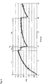
- Fig. 6 is a view illustrating a first operation result of the measuring apparatus 1 according to the first embodiment of the present invention.
- Fig. 7 is a view illustrating a second operation result of the measuring apparatus 1 according to the first embodiment of the present invention.
- a change in power supply voltage Vout during each operation is expressed along a time axis when the CT 2 is constructed with the first CT.
- the change in power supply voltage Vout during each operation is expressed along the time axis when the CT 2 is constructed with the second CT.
- a voltage change in the initial charging (Step S4 in Fig. 5 ) is indicated during a period T1 in Figs. 6 and 7 .
- the voltage change in starting the MPU 12 (Step S6 in Fig. 5 ) is indicated during a period T2.
- the voltage change in performing the measuring processing and the transmission processing (Steps S10 and S14 in Fig. 5 ) is indicated during a period T3.
- the voltage change in the standby state of the MPU 12 (Step S16 in Fig. 5 ) is indicated during a period T4.
- the power supply voltage Vout drops steeply by the measuring processing and the transmission processing.
- the subsequent measuring processing and transmission processing can properly be performed by performing the charging for a certain period (T4).
- the switching circuit 7 is constructed with the low-power-consumption FETs 71 and 72, so that the necessary processing (such as the measuring processing and the transmission processing) can be performed without influencing the supply of the power to the power supply circuit 6 even if the switching control is performed.
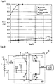
- Fig. 8 is a graph illustrating a measurement error of each of measuring apparatuses according to the first embodiment of the present invention and first and second comparative examples.
- the secondary circuit is constructed with the circuit 103 in Fig. 17
- the CT 2 is constructed with the first CT.
- the secondary circuit is constructed with the circuit 103 in Fig. 17
- the CT 2 is constructed with the second CT.
- the CT 2 is constructed with the first CT.
- a horizontal axis indicates the power supply voltage Vout (V), and a vertical axis indicates the measurement error (%).
- the measurement error indicates an error with a measured value (ideal value) in the measuring circuit 104 of Fig. 4 .
- the measuring circuit 104 has the configuration in which the rectifier circuit 5 and the power supply circuit 6 are not included in the subsequent stage of the measuring circuit 4.
- a line L11 indicates the measurement error in the first comparative example
- a line L12 indicates the measurement error in the second comparative example.
- a line L10 indicates the measurement error in the first embodiment.
- the output current Is is influenced for the secondary circuit 103 that does not include the switching circuit 7.
- the error exceeds 70% even at a time point the power supply voltage Vout is 0 V.
- the line L12 even for the second CT having the good transfer characteristic, the error increases with increasing power supply voltage Vout, and the error becomes about 10% near the saturation voltage.
- the measurement error is about 0% irrespective of the power supply voltage even if the CT 2 is constructed with the first CT having the poor transfer characteristic.
- the current can accurately be measured irrespective of the transfer characteristic of the CT 2. As a result, downsizing and cost reduction of the apparatus can be achieved.
- the switching circuit 7 is constructed with the pair of p-type FETs.
- the switching circuit 7 can also be constructed with an n-type FET. Only a different point with the first embodiment will be described below.
- Fig. 9 is a view illustrating a configuration of a secondary circuit 3A according to a second embodiment of the present invention.
- the same configuration as the secondary circuit 3 in Fig. 1 is designated by the same numeral. Accordingly, the overlapping description is not repeated. The same holds true for the subsequent embodiments.
- the secondary circuit 3A includes a switching circuit 7A instead of the switching circuit 7 of the first embodiment.
- the position to which the switching circuit 7A is connected is identical to that of the first embodiment.
- the switching circuit 7A includes a pair of n-type FETs 71A and 72A having the identical polarity.
- the drain of the FET 71A is connected to the end 7a of the switching circuit 7.
- the source of the FET 71A is connected to the source of the FET 72A while a predetermined voltage Vpull_down is supplied to the source of the FET 71A.
- the drain of the FET 72A is connected to the end 7b of the switching circuit 7.
- the predetermined voltage Vpull_down is provided to the gate of the FET 72A.
- the control signal is provided to the gates of the FETs 71A and 72A from the switching controller 122 of the MPU 12.
- the control signal is provided to the gate of the FET 72A through the resistor 73.
- the predetermined voltage Vpull_down applied to the connection portion of the FETs 71A and 72A is also decided between the ground potential (0 V) and the power supply voltage Vout.
- the p-type or n-type FET is used as the switching element.
- the FET not only the FET but also a bipolar transistor may be used as the switching element.
- a configuration in which the detection resistor is located between the ground potential and the rectifying element in the secondary circuit will be described in a third embodiment.
- the switching circuit is provided in the connection portion between the measuring circuit (detection resistor) and the rectifier circuit. Only a different point with the first embodiment will be described below.
- Fig. 10 is a view illustrating a configuration of a secondary circuit 3B according to the third embodiment of the present invention.
- the secondary circuit 3B includes a measuring circuit 4A and a switching circuit 7B instead of the measuring circuit 4 and the switching circuit 7 of the first embodiment.
- the measuring circuit 4A includes a detection resistor 41 connected to an anode side 5c of the rectifying element 51 and a detection resistor 42 connected to an anode side 5d of the rectifying element 54.
- the rectifying element 51 is a diode on the ground side of the first rectifier circuit.
- the rectifying element 54 is a diode on the ground side of the second rectifier circuit. That is, one end is grounded in both the detection resistors 41 and 42.
- the voltage detector 11 detects the voltage at each of the detection resistors 41 and 42.
- the measurement processor 121 Fig. 1 ) of the MPU 12 measures the power based on each voltage.
- the detection resistors 41 and 42 are selected such that the voltage during the measurement does not exceed the power supply voltage Vout.
- the switching circuit 7B includes the n-type FETs 71A and 72A.
- the FET 71A is connected between the terminal 21 of the CT 2 and the anode side 5c of the rectifying element 51, namely, between the terminal 21 of the CT 2 and the other end of the detection resistor 41.
- the FET 72A is connected between the terminal 22 of the CT 2 and the anode side 5d of the rectifying element 54, namely, between the terminal 22 of the CT 2 and the other end of the detection resistor 42.
- the control signal is provided to the gates of the FETs 71A and 72A.
- the resistor 73 is connected between the gates of the FETs 71A and 72A and the ground.
- the switching controller 122 puts the FETs 71A and 72A into the non-conduction state during the non-measurement, and puts the FETs 71A and 72A into the conduction state during the measurement. Therefore, during the non-measurement, the secondary circuit 3B is put into the state constituting a circuit that inputs the outputs of the first and second rectifier circuits to the power supply circuit 6. During the measurement, the secondary circuit 3B is put into the state constituting a circuit that directly inputs the output of the measuring circuit 4A to the CT 2.
- the measuring circuit 4A does not exist between the terminal 21 of the CT 2 and the input terminal 5a of the rectifier circuit 5. Therefore, in the case that the FETs 71A and 72A are put into the non-conduction state during the non-measurement, the measuring circuit 4A can be protected because the high voltage is not applied to the detection resistors 41 and 42.
- the measuring circuit 4A includes the detection resistors 41 and 42 in each of which one end is grounded.
- the measuring circuit 4A may include only one of the detection resistors 41 and 42 in each of which one end is grounded.
- Fig. 11 illustrates a secondary circuit 3C in the case that the measuring circuit 4A may include only one of the detection resistors 41 and 42 in each of which one end is grounded.
- a measuring circuit 4B includes only the detection resistor 41.
- the voltage detector 11 may detect only the voltage at the detection resistor 41.
- the switching circuit 7B is constructed with the n-type FETs 71A and 72A.
- the switching circuit 7B may be constructed with other switching elements such as the p-type FET.
- the switching circuit is constructed with the switching element.
- the switching circuit is not limited to the switching element, but the switching circuit may be constructed with an analog switch or a solid-state relay.
- the configuration of the secondary circuit in which the switching circuit is constructed with the analog switch will be described in a fourth embodiment.
- Figs. 12 and 13 illustrate a configuration of a secondary circuit 3D according to the fourth embodiment of the present invention.
- Figs. 12 and 13 illustrate the passages of the output current Is during the non-measurement and the measurement, respectively.
- the secondary circuit 3D includes a switching circuit 7C instead of the switching circuit 7 of the first embodiment.
- the switching circuit 7C includes switches 74 and 75.
- the switch 75 is connected in parallel to the rectifier circuit 5 on the current output terminal side of the detection resistor 40.
- the switch 74 is connected in series to the detection resistor 40 on the subsequent stage side of the terminal 7a on the side of the detection resistor 40 of the switch 75. More specifically, in the switches 74 and 75, one end is connected onto the current output terminal side (terminal 7a) of the detection resistor 40.
- the other end of the switch 74 is connected to the end 5a of the rectifier circuit 5.
- the other end of the switch 75 is connected to the position (terminal 7b) between the terminal 22 of the CT 2 and the end 5b of the rectifier circuit 5.
- the switching controller 122 puts the switch 75 into the off state, and puts the switch 74 into the on state.
- the terminals 7a and 7b are insulated from each other, and the terminal 7a and the end 5a of the rectifier circuit 5 are electrically connected to each other. Accordingly, the output current Is is passed only on the side of the rectifier circuit 5, and the power is supplied to the power supply circuit 6.
- the switch 75 is put into the on state while the switch 74 is put into the off state.
- the terminals 7a and 7b are electrically connected to each other, and the terminal 7a and the end 5a of the rectifier circuit 5 are insulated from each other. Accordingly, the output current Is is passed through not the rectifier circuit 5, but only the measuring circuit 4.
- the switching circuit is constructed with the pair of analog switches like the fourth embodiment
- the power supply is required to operate the switches.
- the measuring apparatus of the fourth embodiment is provided with a primary battery (not illustrated) in order to operate the switches.
- the output current Is is passed through the detection resistor during the supply of the power (during the non-measurement).
- the output current Is needs not to be passed through the detection resistor during the supply of the power.
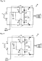
- Fig. 14 is a view illustrating a configuration of a secondary circuit 3E according to a first modification of the fourth embodiment of the present invention.
- the detection resistor 40 is connected in parallel to the rectifier circuit 5. Both ends of the parallel circuit constitute terminals 8a and 8b, respectively.
- the switch 74 is connected between the terminal 8a and the end 5a of the rectifier circuit 5.
- the switch 75 is connected in series to the current output terminal side of the detection resistor 40.
- the switching control of the switching controller 122 ( Fig. 1 ) is identical to that of fourth embodiment.
- the secondary circuit 3E is put into the state constituting a circuit that inputs the outputs of the rectifier circuit 5 to the power supply circuit 6.
- the secondary circuit 3E is put into the state constituting a circuit that directly inputs the output of a measuring circuit 4C to the CT 2.
- a configuration in Fig. 15 may be used in the case that the detection resistor 40 is connected in parallel to the rectifier circuit 5 like the first modification.
- Fig. 15 is a view illustrating a configuration of a secondary circuit 3F according to a second modification of the fourth embodiment of the present invention.
- the position of the switch 74 differs from that in Fig. 14 .
- the predetermined voltage Vpull_up is supplied to a connection point 8c between the detection resistor 40 and the switch 75, and the switch 74 is connected onto the supply passage of the predetermined voltage Vpull_up.
- the switching controller 122 puts the switches 74 and 75 into the off state during the non-measurement, and puts the switches 74 and 75 into the on state during the measurement.
- the voltage Vpull_up is decided between the ground potential (0 V) and the output voltage Vout to the power supply circuit 6.
- the reverse bias voltage is applied to all the rectifying diodes 51 to 54 of the rectifier circuit 5. Therefore, during the measurement, output current Is is passed only onto the side of the detection resistor 40 through the terminal 8a.
- a configuration in Fig. 16 may be used in the case that the detection resistor 40 is connected in parallel to the rectifier circuit 5.
- Fig. 16 is a view illustrating a configuration of a secondary circuit 3G according to a third modification of the fourth embodiment of the present invention.
- the third modification differs from the configuration of Fig. 15 in the position of the switch 74.
- the predetermined voltage Vpull_up is also applied to the connection point 8c between the detection resistor 40 and the switch 75.
- the switch 74 is connected in series to the current input terminal side of the detection resistor 40. In this case, the switching control of the switches 74 and 75 is similar to that of the second modification.
- the power supply circuit is electrically separated from the measuring circuit (detection resistor) during the measurement, so that the measurement accuracy can be improved. Accordingly, the measurement of the current and the supply of the power can properly be performed only by mounting one compact CT having the high magnetic resistance as the element transforming the physical amount into the current. As a result, the downsizing and cost reduction of the measuring apparatus can be achieved.
- the CT transforms the power into the current by way of example.
- another physical amount may be transformed into the current by energy harvesting.
- the measuring target physical amounts include i) wind-force amount, ii) hydraulic power amount, iii) heat amount, and iv) illuminance.
- the measurement processor 121 in Fig. 1 detects the current or voltage using the measuring circuit to measure (calculates) each physical amount.
- a motor is used as a transformation element.
- a Peltier element is used as the transformation element.
- a photoelectric element is used as the transformation element.
- the measurement accuracy is influenced when the power supply voltage at the subsequent stage increases relative to a power generation amount. More specifically, in the case that the motor is used as the transformation element, sometimes a torque unnecessary for the rotation of the motor is applied by the power supply voltage to decrease the output. In the case that the Peltier element and the photoelectric element are used as the transformation element, similarly to the CT, sometimes the current is not output according to the voltage generated between the elements due to the power supply voltage. Therefore, the kind of the usable element is restricted, and sometimes a freedom degree of product design is largely restricted. On the other hand, the restriction of the usable element is eliminated by using the secondary circuits of the embodiments and modifications. Accordingly, in the embodiments and modifications, the downsizing and cost reduction of the measuring apparatus can be achieved.
Landscapes
- Physics & Mathematics (AREA)
- General Physics & Mathematics (AREA)
- Engineering & Computer Science (AREA)
- Power Engineering (AREA)
- Measurement Of Current Or Voltage (AREA)
- Dc-Dc Converters (AREA)
Claims (7)
- Messvorrichtung (1), umfassend:einen Transformator (2), der dafür ausgelegt ist, eine physikalische Größe in einen Strom umzuwandeln;eine Messschaltung (4), die dafür ausgelegt ist, einen Ausgangsstrom des Transformators (2) der physikalischen Größe zu messen;eine Stromversorgungsschaltung (6), die dafür ausgelegt ist, als Eingang in die Stromversorgungsschaltung (6) einen Ausgangsstrom der Messschaltung (4) zu erhalten;eine Schalteinrichtung (7), die dafür ausgelegt ist, zwischen einem ersten Zustand und einem zweiten Zustand umzuschalten, wobei der erste Zustand eine Schaltung darstellt, die den Ausgangsstrom der Messschaltung (4) in die Stromversorgungsschaltung (6) eingibt, wobei der zweite Zustand eine Schaltung darstellt, die den Ausgangsstrom der Messschaltung (4) direkt in den Transformator der physikalischen Größe eingibt;eine Gleichrichterschaltung (5), die dafür ausgelegt ist, den Ausgangsstrom, der vom Transformator (2) für die physikalische Größe transformiert wurde, in einen Gleichstrom gleichzurichten,wobei der Ausgangsstrom des Transformators (2) der physikalischen Größe ein Wechselstrom ist; undeinen Schaltregler (122), der dafür ausgelegt ist, von der Stromversorgungsschaltung (6) so angetrieben zu werden, dass er die Schalteinrichtung (7) steuert, wobei der Schaltregler (122) dafür ausgelegt ist, die Schalteinrichtung (7) derart zu steuern, dass die Schalteinrichtung (7) während des Wartens, das ein Zeitabschnitt ist, während dessen mindestens eine Messperiode ausgeklammert ist, im ersten Zustand ist, und der Schaltregler ist dafür ausgelegt, die Schalteinrichtung (7) derart zu steuern, dass die Schalteinrichtung (7) während der Messung, die der Zeitabschnitt der Messung ist, im zweiten Zustand ist,wobei der Transformator (2) der physikalischen Größe einen Verbindungsanschluss (21, 22) umfasst, der dazu verwendet wird, einen Wechselstrom herauszuführen,die Messschaltung (4) umfasst einen Detektor (40), der dafür ausgelegt ist, den Strom zu erfassen,ein Stromeingangsanschluss des Detektors (40) ist mit einem Ende (21) des Verbindungsanschlusses (21, 22) verbunden,die Gleichrichterschaltung (5) ist an eine Stromausgangsanschlussseite des Detektors (40) angeschlossen, unddie Schalteinrichtung (7) ist zwischen der Stromausgangsanschlussseite des Detektors (40) und der Gleichrichterschaltung (5) angeschlossen.
- Messvorrichtung (1) nach Anspruch 1, wobei die Schalteinrichtung (7) erste und zweite Schaltelemente (71, 72) umfasst, die eine identische Polarität haben, wobei jedes der ersten und zweiten Schaltelemente (71, 72) an einen Stromausgangsanschluss des Detektors (40) und das andere Ende (22) des Verbindungsanschlusses (21, 22) des Transformators (2) der physikalischen Größe angeschlossen ist.
- Messvorrichtung (1) nach Anspruch 2, wobei eine Spannung an einem Kontakt (7a), an dem die ersten und zweiten Schaltelemente (71, 72) mit dem StromAusgangsanschluss des Detektors (40) verbunden sind, zu einem Wert zwischen einem Massepotential und einer Spannung auf einer Eingangsseite der Stromversorgungsschaltung (6) wird, wenn sich die Schalteinrichtung (7) im zweiten Zustand befindet.
- Messvorrichtung (1) nach Anspruch 2 oder 3, wobei der Schaltregler (122) dafür ausgelegt ist, die Schalteinrichtung (7) in den ersten Zustand während des Wartens zu versetzen, indem er die ersten und zweiten Schaltelemente (71, 72) in einen nichtleitenden Zustand versetzt, und der Schaltregler (122) ist dafür ausgelegt, die Schalteinrichtung (7) während der Messung in den zweiten Zustand zu versetzen, indem er die ersten und zweiten Schaltelemente (71, 72) in einen leitenden Zustand versetzt.
- Messvorrichtung (1) nach einem der Ansprüche 2 bis 4, wobei die ersten und zweiten Schaltelemente (71, 72) einen n-Typ- oder p-Typ-FET oder einen bipolaren Transistor umfassen.
- Messvorrichtung (1) nach einem der Ansprüche 1 bis 5, wobei der Transformator (2) für die physikalische Größe mit einem Stromtransformator aufgebaut ist, der dafür ausgelegt ist, einen Strom herauszuführen, der durch eine Stromleitung geführt wird, während der Strom mit einem vorgegebenen Stromtransformationsverhältnis transformiert wird.
- Messverfahren zum Messen eines Stroms in einer Messvorrichtung (1), wobei die Messvorrichtung (1) umfasst:einen Transformator (2) einer physikalischen Größe, der dafür ausgelegt ist, eine physikalische Größe in einen Strom zu transformieren;eine Messschaltung (4), die dafür ausgelegt ist, einen Ausgangsstrom des Transformators (2) der physikalischen Größe zu messen;eine Stromversorgungsschaltung (6), die dafür ausgelegt ist, als Eingabe in die Stromversorgungsschaltung (6) einen Ausgangsstrom der Messschaltung (4) zu erhalten;eine Schalteinrichtung (7), die dafür ausgelegt ist, zwischen einem ersten Zustand und einem zweiten Zustand umzuschalten, wobei der erste Zustand eine Schaltung darstellt, die den Ausgangsstrom der Messschaltung (4) in die Stromversorgungsschaltung (6) eingibt, wobei der zweite Zustand eine Schaltung darstellt, die den Ausgangsstrom der Messschaltung (4) in den Transformator der physikalischen Größe direkt eingibt;eine Gleichrichterschaltung (5), die dafür ausgelegt ist, den Ausgangsstrom, der durch den Transformator (2) der physikalischen Größe transformiert wurde, in einen Gleichstrom gleichzurichten,wobei der Ausgangsstrom des Transformators (2) der physikalischen Größe ein Wechselstrom ist; undeinen Schaltregler (122), der dafür ausgelegt ist, durch die Stromversorgungsschaltung (6) angetrieben zu werden, um die Schalteinrichtung (7) zu steuern,wobei der Schaltregler (122) dafür ausgelegt ist, die Schalteinrichtung (7) derart zu steuern, dass die Schalteinrichtung (7) während des Wartens, die ein Zeitabschnitt ist, bei dem mindestens eine Messperiode ausgeklammert wird, im ersten Zustand ist, und der Schaltregler ist dafür ausgelegt, die Schalteinrichtung (7) derart zu steuern, dass die Schalteinrichtung (7) während der Messung, die ein Zeitabschnitt des Messens ist, im zweiten Zustand ist,wobei der Transformator (2) der physikalischen Größe einen Verbindungsanschluss (21, 22) umfasst, der zum Herausführen eines Wechselstroms verwendet wird, die Messschaltung (4) umfasst einen Detektor (40), der dafür ausgelegt ist, den Strom zu erfassen,ein Stromeingangsterminal des Detektors (40) ist mit einem Ende (21) des Verbindungsanschlusses (21, 22) verbunden,die Gleichrichterschaltung (5) ist an eine Stromausgangsanschlussseite des Detektors (40) angeschlossen, unddie Schalteinrichtung (7) ist zwischen der Stromausgangsanschlussseite des Detektors (40) und der Gleichrichterschaltung (5) angeschlossen,wobei das Messverfahren die folgenden Schritte umfasst: einen Transformationsschritt des Transformierens einer physikalischen Größe in einen Strom mit dem Transformator (2) der physikalischen Größe;einen Schritt des Zuführens eines imTransformationsschritt transformierten Ausgangsstroms zur Stromversorgungsschaltung (6) während des Wartens durch Steuern der Schalteinrichtung (7) in den ersten Zustand; undeinen Schritt zur Messung des Ausgangsstroms, der im Transformationsschritt während der genannten Messperiode mit Ausnahme des Wartens transformiert wird, indem die Schalteinrichtung (7) in den zweiten Zustand gesteuert wird.
Applications Claiming Priority (2)
| Application Number | Priority Date | Filing Date | Title |
|---|---|---|---|
| JP2013052982A JP6171429B2 (ja) | 2013-03-15 | 2013-03-15 | 計測装置および計測方法 |
| PCT/JP2014/051186 WO2014141746A1 (ja) | 2013-03-15 | 2014-01-22 | 計測装置および計測方法 |
Publications (3)
| Publication Number | Publication Date |
|---|---|
| EP2975416A1 EP2975416A1 (de) | 2016-01-20 |
| EP2975416A4 EP2975416A4 (de) | 2017-03-01 |
| EP2975416B1 true EP2975416B1 (de) | 2020-03-11 |
Family
ID=51536423
Family Applications (1)
| Application Number | Title | Priority Date | Filing Date |
|---|---|---|---|
| EP14762751.7A Active EP2975416B1 (de) | 2013-03-15 | 2014-01-22 | Messvorrichtung und messverfahren |
Country Status (6)
| Country | Link |
|---|---|
| US (1) | US9945887B2 (de) |
| EP (1) | EP2975416B1 (de) |
| JP (1) | JP6171429B2 (de) |
| KR (1) | KR101750644B1 (de) |
| CN (1) | CN105026940B (de) |
| WO (1) | WO2014141746A1 (de) |
Families Citing this family (9)
| Publication number | Priority date | Publication date | Assignee | Title |
|---|---|---|---|---|
| CN106330300B (zh) * | 2015-06-30 | 2018-11-27 | 菲尼萨公司 | 空闲状态检测电路、空闲状态检测方法以及有源光纤缆线 |
| JP6650164B2 (ja) * | 2016-02-04 | 2020-02-19 | アルプスアルパイン株式会社 | 自己給電型の電流センサ |
| KR102575279B1 (ko) * | 2016-08-05 | 2023-09-06 | 주식회사 아모센스 | 전원 안정화 장치 및 이를 포함하는 자기유도 전원 공급 시스템 |
| JP6680251B2 (ja) | 2017-03-15 | 2020-04-15 | オムロン株式会社 | 配電網モニタリングシステム |
| JP6903963B2 (ja) | 2017-03-15 | 2021-07-14 | オムロン株式会社 | 配電網モニタリングシステムおよび配電網モニタリング装置 |
| JP6747347B2 (ja) | 2017-03-15 | 2020-08-26 | オムロン株式会社 | 配電網モニタリングシステムおよび配電網モニタリング装置 |
| JP6677197B2 (ja) | 2017-03-15 | 2020-04-08 | オムロン株式会社 | 高調波検出システム |
| KR102270285B1 (ko) * | 2019-10-29 | 2021-06-28 | (주)화인파워엑스 | 무선 온라인 모니터링 시스템을 위한 계기용 변류기의 전원공급장치 |
| TWI780791B (zh) * | 2021-06-25 | 2022-10-11 | 台達電子工業股份有限公司 | 電流檢測電路及其檢測方法 |
Family Cites Families (16)
| Publication number | Priority date | Publication date | Assignee | Title |
|---|---|---|---|---|
| US3260976A (en) * | 1964-06-30 | 1966-07-12 | Gen Electric | Current transformer |
| US4196387A (en) * | 1978-04-17 | 1980-04-01 | Tokyo Shibaura Denki Kabushiki Kaisha | Apparatus for measuring output DC current of rectifier devices |
| JP3728046B2 (ja) * | 1996-06-26 | 2005-12-21 | 沖電気工業株式会社 | 極性反転検出回路 |
| JP3306706B2 (ja) * | 1998-08-20 | 2002-07-24 | 株式会社井上電機製作所 | 電流測定装置 |
| ATE294397T1 (de) | 2000-10-13 | 2005-05-15 | Primarion Inc | System und verfahren zur strommessung |
| JP4258119B2 (ja) * | 2000-10-27 | 2009-04-30 | 富士電機システムズ株式会社 | 電流計測装置 |
| JP3475943B2 (ja) | 2001-06-29 | 2003-12-10 | サンケン電気株式会社 | スイッチング電源装置 |
| US7626378B1 (en) * | 2006-06-21 | 2009-12-01 | Fest Otto P | Signal powered A.C. current transformer electronic measuring circuit |
| JP4320788B1 (ja) | 2008-01-28 | 2009-08-26 | 株式会社村田製作所 | Dc−dcコンバータ |
| JP5030896B2 (ja) * | 2008-08-28 | 2012-09-19 | 東洋電機製造株式会社 | 設備データ収集システム |
| CN201392362Y (zh) | 2009-03-20 | 2010-01-27 | 北京普源精电科技有限公司 | 一种电流测量装置 |
| US9267826B2 (en) * | 2010-05-28 | 2016-02-23 | Schneider Electric It Corporation | System for self-powered, wireless monitoring of electrical current, power and energy |
| KR101153504B1 (ko) * | 2010-09-30 | 2012-06-12 | 한국전력공사 | 복수의 입력신호의 처리가 가능한 전자식 전력량 계산기 및 전력량 계산방법 |
| JP5528999B2 (ja) | 2010-12-15 | 2014-06-25 | 株式会社アドバンテスト | 試験装置 |
| US20130151184A1 (en) * | 2011-12-07 | 2013-06-13 | Infineon Technologies Austria Ag | Meter Device |
| CN103376344B (zh) * | 2012-04-20 | 2016-03-30 | 台达电子工业股份有限公司 | 电流检测装置及电能质量补偿系统 |
-
2013
- 2013-03-15 JP JP2013052982A patent/JP6171429B2/ja active Active
-
2014
- 2014-01-22 WO PCT/JP2014/051186 patent/WO2014141746A1/ja not_active Ceased
- 2014-01-22 KR KR1020157024796A patent/KR101750644B1/ko not_active Expired - Fee Related
- 2014-01-22 US US14/776,840 patent/US9945887B2/en active Active
- 2014-01-22 CN CN201480012921.8A patent/CN105026940B/zh not_active Expired - Fee Related
- 2014-01-22 EP EP14762751.7A patent/EP2975416B1/de active Active
Non-Patent Citations (1)
| Title |
|---|
| None * |
Also Published As
| Publication number | Publication date |
|---|---|
| KR20150119158A (ko) | 2015-10-23 |
| CN105026940A (zh) | 2015-11-04 |
| JP2014178238A (ja) | 2014-09-25 |
| CN105026940B (zh) | 2017-08-25 |
| EP2975416A1 (de) | 2016-01-20 |
| JP6171429B2 (ja) | 2017-08-02 |
| US9945887B2 (en) | 2018-04-17 |
| WO2014141746A1 (ja) | 2014-09-18 |
| EP2975416A4 (de) | 2017-03-01 |
| US20160025778A1 (en) | 2016-01-28 |
| KR101750644B1 (ko) | 2017-06-23 |
Similar Documents
| Publication | Publication Date | Title |
|---|---|---|
| EP2975416B1 (de) | Messvorrichtung und messverfahren | |
| US10199868B2 (en) | Power receiver, non-contact power transmission system, and method of controlling received-power voltage | |
| JP6444477B2 (ja) | スイッチモード電力コンバータ電流検知装置及び方法 | |
| US8300440B2 (en) | AC-DC converter and AC-DC conversion method | |
| CN110336467B (zh) | 同步整流器控制器、开关模式电源和同步整流器控制方法 | |
| US20160268834A1 (en) | Wireless power receiver with dynamically configurable power path | |
| US12519325B2 (en) | Electronic device for carrying out overvoltage protection operation and control method therefor | |
| US9768701B2 (en) | Synchronous rectifier control using sensing of alternating current component | |
| KR20130095906A (ko) | 무선전력 수신장치 및 무선전력 전송 시스템 | |
| US10461632B1 (en) | Current sensing for bridgeless PFC converters | |
| CN107064597B (zh) | 自供电式的电流传感器 | |
| US9106071B2 (en) | Apparatus and methods of bootstrap and over voltage combination clamp for wireless power receiver | |
| JP2002252980A (ja) | 変流器入力型電源装置 | |
| US9660459B2 (en) | Voltage regulator and power receiving apparatus | |
| JP7361457B2 (ja) | スイッチング電源装置 | |
| US8994354B2 (en) | Electronic power converter with ground referenced lossless current sensing | |
| US9048731B2 (en) | Rectifying apparatus | |
| CN113131743A (zh) | 隔离式电源供应器及其二次侧控制电路 | |
| US11606042B1 (en) | Efficient negative-sense detection of synchronous recitifer in voltage converter | |
| US20070200590A1 (en) | Saturation detection circuits | |
| KR20190011598A (ko) | 무선 전력전송장치 및 이를 포함하는 공기청정기 | |
| JP2020014286A (ja) | 電源装置 | |
| CN110311579B (zh) | 通信协议电路与其中的分时电流侦测电路与方法 | |
| KR20200035688A (ko) | 무선 전력 송신 방법 및 장치 | |
| KR20120103292A (ko) | 무접점 전력공급 시스템, 방법, 및 그 기록매체 |
Legal Events
| Date | Code | Title | Description |
|---|---|---|---|
| PUAI | Public reference made under article 153(3) epc to a published international application that has entered the european phase |
Free format text: ORIGINAL CODE: 0009012 |
|
| 17P | Request for examination filed |
Effective date: 20151005 |
|
| AK | Designated contracting states |
Kind code of ref document: A1 Designated state(s): AL AT BE BG CH CY CZ DE DK EE ES FI FR GB GR HR HU IE IS IT LI LT LU LV MC MK MT NL NO PL PT RO RS SE SI SK SM TR |
|
| AX | Request for extension of the european patent |
Extension state: BA ME |
|
| DAX | Request for extension of the european patent (deleted) | ||
| A4 | Supplementary search report drawn up and despatched |
Effective date: 20170130 |
|
| RIC1 | Information provided on ipc code assigned before grant |
Ipc: G01R 15/18 20060101ALI20170124BHEP Ipc: G01R 19/00 20060101AFI20170124BHEP |
|
| GRAP | Despatch of communication of intention to grant a patent |
Free format text: ORIGINAL CODE: EPIDOSNIGR1 |
|
| STAA | Information on the status of an ep patent application or granted ep patent |
Free format text: STATUS: GRANT OF PATENT IS INTENDED |
|
| INTG | Intention to grant announced |
Effective date: 20191004 |
|
| GRAS | Grant fee paid |
Free format text: ORIGINAL CODE: EPIDOSNIGR3 |
|
| GRAA | (expected) grant |
Free format text: ORIGINAL CODE: 0009210 |
|
| STAA | Information on the status of an ep patent application or granted ep patent |
Free format text: STATUS: THE PATENT HAS BEEN GRANTED |
|
| AK | Designated contracting states |
Kind code of ref document: B1 Designated state(s): AL AT BE BG CH CY CZ DE DK EE ES FI FR GB GR HR HU IE IS IT LI LT LU LV MC MK MT NL NO PL PT RO RS SE SI SK SM TR |
|
| REG | Reference to a national code |
Ref country code: GB Ref legal event code: FG4D |
|
| REG | Reference to a national code |
Ref country code: CH Ref legal event code: EP |
|
| REG | Reference to a national code |
Ref country code: AT Ref legal event code: REF Ref document number: 1243809 Country of ref document: AT Kind code of ref document: T Effective date: 20200315 |
|
| REG | Reference to a national code |
Ref country code: DE Ref legal event code: R096 Ref document number: 602014062198 Country of ref document: DE |
|
| REG | Reference to a national code |
Ref country code: IE Ref legal event code: FG4D |
|
| PG25 | Lapsed in a contracting state [announced via postgrant information from national office to epo] |
Ref country code: RS Free format text: LAPSE BECAUSE OF FAILURE TO SUBMIT A TRANSLATION OF THE DESCRIPTION OR TO PAY THE FEE WITHIN THE PRESCRIBED TIME-LIMIT Effective date: 20200311 Ref country code: FI Free format text: LAPSE BECAUSE OF FAILURE TO SUBMIT A TRANSLATION OF THE DESCRIPTION OR TO PAY THE FEE WITHIN THE PRESCRIBED TIME-LIMIT Effective date: 20200311 Ref country code: NO Free format text: LAPSE BECAUSE OF FAILURE TO SUBMIT A TRANSLATION OF THE DESCRIPTION OR TO PAY THE FEE WITHIN THE PRESCRIBED TIME-LIMIT Effective date: 20200611 |
|
| REG | Reference to a national code |
Ref country code: NL Ref legal event code: MP Effective date: 20200311 |
|
| PG25 | Lapsed in a contracting state [announced via postgrant information from national office to epo] |
Ref country code: GR Free format text: LAPSE BECAUSE OF FAILURE TO SUBMIT A TRANSLATION OF THE DESCRIPTION OR TO PAY THE FEE WITHIN THE PRESCRIBED TIME-LIMIT Effective date: 20200612 Ref country code: HR Free format text: LAPSE BECAUSE OF FAILURE TO SUBMIT A TRANSLATION OF THE DESCRIPTION OR TO PAY THE FEE WITHIN THE PRESCRIBED TIME-LIMIT Effective date: 20200311 Ref country code: LV Free format text: LAPSE BECAUSE OF FAILURE TO SUBMIT A TRANSLATION OF THE DESCRIPTION OR TO PAY THE FEE WITHIN THE PRESCRIBED TIME-LIMIT Effective date: 20200311 Ref country code: SE Free format text: LAPSE BECAUSE OF FAILURE TO SUBMIT A TRANSLATION OF THE DESCRIPTION OR TO PAY THE FEE WITHIN THE PRESCRIBED TIME-LIMIT Effective date: 20200311 Ref country code: BG Free format text: LAPSE BECAUSE OF FAILURE TO SUBMIT A TRANSLATION OF THE DESCRIPTION OR TO PAY THE FEE WITHIN THE PRESCRIBED TIME-LIMIT Effective date: 20200611 |
|
| REG | Reference to a national code |
Ref country code: LT Ref legal event code: MG4D |
|
| PG25 | Lapsed in a contracting state [announced via postgrant information from national office to epo] |
Ref country code: NL Free format text: LAPSE BECAUSE OF FAILURE TO SUBMIT A TRANSLATION OF THE DESCRIPTION OR TO PAY THE FEE WITHIN THE PRESCRIBED TIME-LIMIT Effective date: 20200311 |
|
| PG25 | Lapsed in a contracting state [announced via postgrant information from national office to epo] |
Ref country code: LT Free format text: LAPSE BECAUSE OF FAILURE TO SUBMIT A TRANSLATION OF THE DESCRIPTION OR TO PAY THE FEE WITHIN THE PRESCRIBED TIME-LIMIT Effective date: 20200311 Ref country code: CZ Free format text: LAPSE BECAUSE OF FAILURE TO SUBMIT A TRANSLATION OF THE DESCRIPTION OR TO PAY THE FEE WITHIN THE PRESCRIBED TIME-LIMIT Effective date: 20200311 Ref country code: RO Free format text: LAPSE BECAUSE OF FAILURE TO SUBMIT A TRANSLATION OF THE DESCRIPTION OR TO PAY THE FEE WITHIN THE PRESCRIBED TIME-LIMIT Effective date: 20200311 Ref country code: SK Free format text: LAPSE BECAUSE OF FAILURE TO SUBMIT A TRANSLATION OF THE DESCRIPTION OR TO PAY THE FEE WITHIN THE PRESCRIBED TIME-LIMIT Effective date: 20200311 Ref country code: EE Free format text: LAPSE BECAUSE OF FAILURE TO SUBMIT A TRANSLATION OF THE DESCRIPTION OR TO PAY THE FEE WITHIN THE PRESCRIBED TIME-LIMIT Effective date: 20200311 Ref country code: SM Free format text: LAPSE BECAUSE OF FAILURE TO SUBMIT A TRANSLATION OF THE DESCRIPTION OR TO PAY THE FEE WITHIN THE PRESCRIBED TIME-LIMIT Effective date: 20200311 Ref country code: IS Free format text: LAPSE BECAUSE OF FAILURE TO SUBMIT A TRANSLATION OF THE DESCRIPTION OR TO PAY THE FEE WITHIN THE PRESCRIBED TIME-LIMIT Effective date: 20200711 Ref country code: PT Free format text: LAPSE BECAUSE OF FAILURE TO SUBMIT A TRANSLATION OF THE DESCRIPTION OR TO PAY THE FEE WITHIN THE PRESCRIBED TIME-LIMIT Effective date: 20200805 |
|
| REG | Reference to a national code |
Ref country code: AT Ref legal event code: MK05 Ref document number: 1243809 Country of ref document: AT Kind code of ref document: T Effective date: 20200311 |
|
| REG | Reference to a national code |
Ref country code: DE Ref legal event code: R097 Ref document number: 602014062198 Country of ref document: DE |
|
| PLBE | No opposition filed within time limit |
Free format text: ORIGINAL CODE: 0009261 |
|
| STAA | Information on the status of an ep patent application or granted ep patent |
Free format text: STATUS: NO OPPOSITION FILED WITHIN TIME LIMIT |
|
| PG25 | Lapsed in a contracting state [announced via postgrant information from national office to epo] |
Ref country code: ES Free format text: LAPSE BECAUSE OF FAILURE TO SUBMIT A TRANSLATION OF THE DESCRIPTION OR TO PAY THE FEE WITHIN THE PRESCRIBED TIME-LIMIT Effective date: 20200311 Ref country code: DK Free format text: LAPSE BECAUSE OF FAILURE TO SUBMIT A TRANSLATION OF THE DESCRIPTION OR TO PAY THE FEE WITHIN THE PRESCRIBED TIME-LIMIT Effective date: 20200311 Ref country code: AT Free format text: LAPSE BECAUSE OF FAILURE TO SUBMIT A TRANSLATION OF THE DESCRIPTION OR TO PAY THE FEE WITHIN THE PRESCRIBED TIME-LIMIT Effective date: 20200311 Ref country code: IT Free format text: LAPSE BECAUSE OF FAILURE TO SUBMIT A TRANSLATION OF THE DESCRIPTION OR TO PAY THE FEE WITHIN THE PRESCRIBED TIME-LIMIT Effective date: 20200311 |
|
| 26N | No opposition filed |
Effective date: 20201214 |
|
| PG25 | Lapsed in a contracting state [announced via postgrant information from national office to epo] |
Ref country code: SI Free format text: LAPSE BECAUSE OF FAILURE TO SUBMIT A TRANSLATION OF THE DESCRIPTION OR TO PAY THE FEE WITHIN THE PRESCRIBED TIME-LIMIT Effective date: 20200311 Ref country code: PL Free format text: LAPSE BECAUSE OF FAILURE TO SUBMIT A TRANSLATION OF THE DESCRIPTION OR TO PAY THE FEE WITHIN THE PRESCRIBED TIME-LIMIT Effective date: 20200311 |
|
| PG25 | Lapsed in a contracting state [announced via postgrant information from national office to epo] |
Ref country code: MC Free format text: LAPSE BECAUSE OF FAILURE TO SUBMIT A TRANSLATION OF THE DESCRIPTION OR TO PAY THE FEE WITHIN THE PRESCRIBED TIME-LIMIT Effective date: 20200311 |
|
| REG | Reference to a national code |
Ref country code: CH Ref legal event code: PL |
|
| PG25 | Lapsed in a contracting state [announced via postgrant information from national office to epo] |
Ref country code: LU Free format text: LAPSE BECAUSE OF NON-PAYMENT OF DUE FEES Effective date: 20210122 |
|
| REG | Reference to a national code |
Ref country code: BE Ref legal event code: MM Effective date: 20210131 |
|
| PG25 | Lapsed in a contracting state [announced via postgrant information from national office to epo] |
Ref country code: LI Free format text: LAPSE BECAUSE OF NON-PAYMENT OF DUE FEES Effective date: 20210131 Ref country code: CH Free format text: LAPSE BECAUSE OF NON-PAYMENT OF DUE FEES Effective date: 20210131 |
|
| PG25 | Lapsed in a contracting state [announced via postgrant information from national office to epo] |
Ref country code: IE Free format text: LAPSE BECAUSE OF NON-PAYMENT OF DUE FEES Effective date: 20210122 |
|
| PGFP | Annual fee paid to national office [announced via postgrant information from national office to epo] |
Ref country code: GB Payment date: 20211206 Year of fee payment: 9 Ref country code: FR Payment date: 20211217 Year of fee payment: 9 |
|
| PGFP | Annual fee paid to national office [announced via postgrant information from national office to epo] |
Ref country code: DE Payment date: 20211130 Year of fee payment: 9 |
|
| PG25 | Lapsed in a contracting state [announced via postgrant information from national office to epo] |
Ref country code: BE Free format text: LAPSE BECAUSE OF NON-PAYMENT OF DUE FEES Effective date: 20210131 |
|
| PG25 | Lapsed in a contracting state [announced via postgrant information from national office to epo] |
Ref country code: HU Free format text: LAPSE BECAUSE OF FAILURE TO SUBMIT A TRANSLATION OF THE DESCRIPTION OR TO PAY THE FEE WITHIN THE PRESCRIBED TIME-LIMIT; INVALID AB INITIO Effective date: 20140122 |
|
| PG25 | Lapsed in a contracting state [announced via postgrant information from national office to epo] |
Ref country code: CY Free format text: LAPSE BECAUSE OF FAILURE TO SUBMIT A TRANSLATION OF THE DESCRIPTION OR TO PAY THE FEE WITHIN THE PRESCRIBED TIME-LIMIT Effective date: 20200311 |
|
| REG | Reference to a national code |
Ref country code: DE Ref legal event code: R119 Ref document number: 602014062198 Country of ref document: DE |
|
| GBPC | Gb: european patent ceased through non-payment of renewal fee |
Effective date: 20230122 |
|
| PG25 | Lapsed in a contracting state [announced via postgrant information from national office to epo] |
Ref country code: GB Free format text: LAPSE BECAUSE OF NON-PAYMENT OF DUE FEES Effective date: 20230122 Ref country code: DE Free format text: LAPSE BECAUSE OF NON-PAYMENT OF DUE FEES Effective date: 20230801 |
|
| PG25 | Lapsed in a contracting state [announced via postgrant information from national office to epo] |
Ref country code: FR Free format text: LAPSE BECAUSE OF NON-PAYMENT OF DUE FEES Effective date: 20230131 |
|
| PG25 | Lapsed in a contracting state [announced via postgrant information from national office to epo] |
Ref country code: MK Free format text: LAPSE BECAUSE OF FAILURE TO SUBMIT A TRANSLATION OF THE DESCRIPTION OR TO PAY THE FEE WITHIN THE PRESCRIBED TIME-LIMIT Effective date: 20200311 |
|
| PG25 | Lapsed in a contracting state [announced via postgrant information from national office to epo] |
Ref country code: MT Free format text: LAPSE BECAUSE OF FAILURE TO SUBMIT A TRANSLATION OF THE DESCRIPTION OR TO PAY THE FEE WITHIN THE PRESCRIBED TIME-LIMIT Effective date: 20200311 |
|
| PG25 | Lapsed in a contracting state [announced via postgrant information from national office to epo] |
Ref country code: TR Free format text: LAPSE BECAUSE OF FAILURE TO SUBMIT A TRANSLATION OF THE DESCRIPTION OR TO PAY THE FEE WITHIN THE PRESCRIBED TIME-LIMIT Effective date: 20200311 |