EP2978023B1 - Photoelektronisches Bildsensor - Google Patents
Photoelektronisches Bildsensor Download PDFInfo
- Publication number
- EP2978023B1 EP2978023B1 EP15152529.2A EP15152529A EP2978023B1 EP 2978023 B1 EP2978023 B1 EP 2978023B1 EP 15152529 A EP15152529 A EP 15152529A EP 2978023 B1 EP2978023 B1 EP 2978023B1
- Authority
- EP
- European Patent Office
- Prior art keywords
- light
- absorption
- absorption material
- layer
- type light
- Prior art date
- Legal status (The legal status is an assumption and is not a legal conclusion. Google has not performed a legal analysis and makes no representation as to the accuracy of the status listed.)
- Active
Links
Images




Classifications
-
- H—ELECTRICITY
- H10—SEMICONDUCTOR DEVICES; ELECTRIC SOLID-STATE DEVICES NOT OTHERWISE PROVIDED FOR
- H10K—ORGANIC ELECTRIC SOLID-STATE DEVICES
- H10K39/00—Integrated devices, or assemblies of multiple devices, comprising at least one organic radiation-sensitive element covered by group H10K30/00
-
- C—CHEMISTRY; METALLURGY
- C09—DYES; PAINTS; POLISHES; NATURAL RESINS; ADHESIVES; COMPOSITIONS NOT OTHERWISE PROVIDED FOR; APPLICATIONS OF MATERIALS NOT OTHERWISE PROVIDED FOR
- C09K—MATERIALS FOR MISCELLANEOUS APPLICATIONS, NOT PROVIDED FOR ELSEWHERE
- C09K11/00—Luminescent materials, e.g. electroluminescent or chemiluminescent
- C09K11/06—Luminescent materials, e.g. electroluminescent or chemiluminescent containing organic luminescent materials
-
- H—ELECTRICITY
- H10—SEMICONDUCTOR DEVICES; ELECTRIC SOLID-STATE DEVICES NOT OTHERWISE PROVIDED FOR
- H10F—INORGANIC SEMICONDUCTOR DEVICES SENSITIVE TO INFRARED RADIATION, LIGHT, ELECTROMAGNETIC RADIATION OF SHORTER WAVELENGTH OR CORPUSCULAR RADIATION
- H10F39/00—Integrated devices, or assemblies of multiple devices, comprising at least one element covered by group H10F30/00, e.g. radiation detectors comprising photodiode arrays
- H10F39/10—Integrated devices
- H10F39/12—Image sensors
-
- H—ELECTRICITY
- H10—SEMICONDUCTOR DEVICES; ELECTRIC SOLID-STATE DEVICES NOT OTHERWISE PROVIDED FOR
- H10K—ORGANIC ELECTRIC SOLID-STATE DEVICES
- H10K30/00—Organic devices sensitive to infrared radiation, light, electromagnetic radiation of shorter wavelength or corpuscular radiation
- H10K30/20—Organic devices sensitive to infrared radiation, light, electromagnetic radiation of shorter wavelength or corpuscular radiation comprising organic-organic junctions, e.g. donor-acceptor junctions
-
- H—ELECTRICITY
- H10—SEMICONDUCTOR DEVICES; ELECTRIC SOLID-STATE DEVICES NOT OTHERWISE PROVIDED FOR
- H10K—ORGANIC ELECTRIC SOLID-STATE DEVICES
- H10K30/00—Organic devices sensitive to infrared radiation, light, electromagnetic radiation of shorter wavelength or corpuscular radiation
- H10K30/30—Organic devices sensitive to infrared radiation, light, electromagnetic radiation of shorter wavelength or corpuscular radiation comprising bulk heterojunctions, e.g. interpenetrating networks of donor and acceptor material domains
-
- H—ELECTRICITY
- H10—SEMICONDUCTOR DEVICES; ELECTRIC SOLID-STATE DEVICES NOT OTHERWISE PROVIDED FOR
- H10K—ORGANIC ELECTRIC SOLID-STATE DEVICES
- H10K30/00—Organic devices sensitive to infrared radiation, light, electromagnetic radiation of shorter wavelength or corpuscular radiation
- H10K30/40—Organic devices sensitive to infrared radiation, light, electromagnetic radiation of shorter wavelength or corpuscular radiation comprising a p-i-n structure, e.g. having a perovskite absorber between p-type and n-type charge transport layers
-
- H—ELECTRICITY
- H10—SEMICONDUCTOR DEVICES; ELECTRIC SOLID-STATE DEVICES NOT OTHERWISE PROVIDED FOR
- H10K—ORGANIC ELECTRIC SOLID-STATE DEVICES
- H10K30/00—Organic devices sensitive to infrared radiation, light, electromagnetic radiation of shorter wavelength or corpuscular radiation
- H10K30/50—Photovoltaic [PV] devices
- H10K30/57—Photovoltaic [PV] devices comprising multiple junctions, e.g. tandem PV cells
-
- H—ELECTRICITY
- H10—SEMICONDUCTOR DEVICES; ELECTRIC SOLID-STATE DEVICES NOT OTHERWISE PROVIDED FOR
- H10K—ORGANIC ELECTRIC SOLID-STATE DEVICES
- H10K30/00—Organic devices sensitive to infrared radiation, light, electromagnetic radiation of shorter wavelength or corpuscular radiation
- H10K30/80—Constructional details
- H10K30/81—Electrodes
- H10K30/82—Transparent electrodes, e.g. indium tin oxide [ITO] electrodes
-
- H—ELECTRICITY
- H10—SEMICONDUCTOR DEVICES; ELECTRIC SOLID-STATE DEVICES NOT OTHERWISE PROVIDED FOR
- H10K—ORGANIC ELECTRIC SOLID-STATE DEVICES
- H10K30/00—Organic devices sensitive to infrared radiation, light, electromagnetic radiation of shorter wavelength or corpuscular radiation
- H10K30/80—Constructional details
- H10K30/87—Light-trapping means
-
- H—ELECTRICITY
- H10—SEMICONDUCTOR DEVICES; ELECTRIC SOLID-STATE DEVICES NOT OTHERWISE PROVIDED FOR
- H10K—ORGANIC ELECTRIC SOLID-STATE DEVICES
- H10K39/00—Integrated devices, or assemblies of multiple devices, comprising at least one organic radiation-sensitive element covered by group H10K30/00
- H10K39/30—Devices controlled by radiation
- H10K39/32—Organic image sensors
-
- H—ELECTRICITY
- H10—SEMICONDUCTOR DEVICES; ELECTRIC SOLID-STATE DEVICES NOT OTHERWISE PROVIDED FOR
- H10K—ORGANIC ELECTRIC SOLID-STATE DEVICES
- H10K50/00—Organic light-emitting devices
-
- H—ELECTRICITY
- H10—SEMICONDUCTOR DEVICES; ELECTRIC SOLID-STATE DEVICES NOT OTHERWISE PROVIDED FOR
- H10K—ORGANIC ELECTRIC SOLID-STATE DEVICES
- H10K85/00—Organic materials used in the body or electrodes of devices covered by this subclass
- H10K85/40—Organosilicon compounds, e.g. TIPS pentacene
-
- H—ELECTRICITY
- H10—SEMICONDUCTOR DEVICES; ELECTRIC SOLID-STATE DEVICES NOT OTHERWISE PROVIDED FOR
- H10H—INORGANIC LIGHT-EMITTING SEMICONDUCTOR DEVICES HAVING POTENTIAL BARRIERS
- H10H20/00—Individual inorganic light-emitting semiconductor devices having potential barriers, e.g. light-emitting diodes [LED]
- H10H20/80—Constructional details
- H10H20/81—Bodies
- H10H20/811—Bodies having quantum effect structures or superlattices, e.g. tunnel junctions
- H10H20/812—Bodies having quantum effect structures or superlattices, e.g. tunnel junctions within the light-emitting regions, e.g. having quantum confinement structures
-
- H—ELECTRICITY
- H10—SEMICONDUCTOR DEVICES; ELECTRIC SOLID-STATE DEVICES NOT OTHERWISE PROVIDED FOR
- H10K—ORGANIC ELECTRIC SOLID-STATE DEVICES
- H10K30/00—Organic devices sensitive to infrared radiation, light, electromagnetic radiation of shorter wavelength or corpuscular radiation
- H10K30/80—Constructional details
- H10K30/84—Layers having high charge carrier mobility
- H10K30/85—Layers having high electron mobility, e.g. electron-transporting layers or hole-blocking layers
-
- H—ELECTRICITY
- H10—SEMICONDUCTOR DEVICES; ELECTRIC SOLID-STATE DEVICES NOT OTHERWISE PROVIDED FOR
- H10K—ORGANIC ELECTRIC SOLID-STATE DEVICES
- H10K30/00—Organic devices sensitive to infrared radiation, light, electromagnetic radiation of shorter wavelength or corpuscular radiation
- H10K30/80—Constructional details
- H10K30/84—Layers having high charge carrier mobility
- H10K30/86—Layers having high hole mobility, e.g. hole-transporting layers or electron-blocking layers
-
- H—ELECTRICITY
- H10—SEMICONDUCTOR DEVICES; ELECTRIC SOLID-STATE DEVICES NOT OTHERWISE PROVIDED FOR
- H10K—ORGANIC ELECTRIC SOLID-STATE DEVICES
- H10K85/00—Organic materials used in the body or electrodes of devices covered by this subclass
- H10K85/20—Carbon compounds, e.g. carbon nanotubes or fullerenes
- H10K85/211—Fullerenes, e.g. C60
-
- H—ELECTRICITY
- H10—SEMICONDUCTOR DEVICES; ELECTRIC SOLID-STATE DEVICES NOT OTHERWISE PROVIDED FOR
- H10K—ORGANIC ELECTRIC SOLID-STATE DEVICES
- H10K85/00—Organic materials used in the body or electrodes of devices covered by this subclass
- H10K85/60—Organic compounds having low molecular weight
- H10K85/649—Aromatic compounds comprising a hetero atom
- H10K85/655—Aromatic compounds comprising a hetero atom comprising only sulfur as heteroatom
-
- H—ELECTRICITY
- H10—SEMICONDUCTOR DEVICES; ELECTRIC SOLID-STATE DEVICES NOT OTHERWISE PROVIDED FOR
- H10W—GENERIC PACKAGES, INTERCONNECTIONS, CONNECTORS OR OTHER CONSTRUCTIONAL DETAILS OF DEVICES COVERED BY CLASS H10
- H10W90/00—Package configurations
-
- Y—GENERAL TAGGING OF NEW TECHNOLOGICAL DEVELOPMENTS; GENERAL TAGGING OF CROSS-SECTIONAL TECHNOLOGIES SPANNING OVER SEVERAL SECTIONS OF THE IPC; TECHNICAL SUBJECTS COVERED BY FORMER USPC CROSS-REFERENCE ART COLLECTIONS [XRACs] AND DIGESTS
- Y02—TECHNOLOGIES OR APPLICATIONS FOR MITIGATION OR ADAPTATION AGAINST CLIMATE CHANGE
- Y02E—REDUCTION OF GREENHOUSE GAS [GHG] EMISSIONS, RELATED TO ENERGY GENERATION, TRANSMISSION OR DISTRIBUTION
- Y02E10/00—Energy generation through renewable energy sources
- Y02E10/50—Photovoltaic [PV] energy
- Y02E10/549—Organic PV cells
Definitions
- the present invention concerns an image sensor.
- a photoelectronic device typically converts light into an electrical signal using photoelectronic effects, may include a photodiode, a phototransistor, and the like, and may be applied to an image sensor, a solar cell, and the like.
- An image sensor including a photodiode requires high resolution and thus a small pixel.
- silicon photodiodes are widely used, but typically exhibit deteriorated sensitivity because of a small absorption area due to small pixels. Accordingly, an organic material that is capable of replacing silicon has been researched.
- an organic material that is capable of replacing silicon may have a high extinction coefficient, or light absorption power, and may selectively absorb light in a particular wavelength region depending on a molecular structure, and thus may replace both a photodiode and a color filter.
- the organic material may have an improved sensitivity and may contribute to higher device integration.
- US 2006/027801 discloses a device having a first electrode, a second electrode, a first photoactive region having a characteristic absorption wavelength ⁇ 1 and a second photoactive region having a characteristic absorption wavelength ⁇ 2 .
- the photoactive regions are disposed between the first and second electrodes, and further positioned on the same side of a reflective layer, such that the first photoactive region is closer to the reflective layer than the second photoactive region.
- US 2005/205903 discloses an imaging element having a photoelectric conversion film which has a laminated structure comprising a p-type semiconductor layer and an n-type semiconductor layer between a pair of electrodes, wherein at least one of the p-type semiconductor and the n-type semiconductor contains an organic compound with controlled orientation; a photoelectric conversion film having at least one organic dye compound, wherein the organic dye compound forms a J aggregate, or the angle between the spectral absorption transition dipolar moment of the organic dye compound and the photoelectric conversion film plane is 40° or less, a photoelectric conversion element and an imaging element; and a method of applying an electric field thereto, and an imaging element which comprises a photoelectric conversion film (a photosensitive layer) having a bulk heterojunction layer as an intermediate layer, or a photoelectric conversion film having two or more repeating structure units of a pn junction layer comprising a p-type semiconductor layer and an n-type semiconductor layer between a pair of electrodes.
- the present invention concerns an image sensor in accordance with claim 1.
- the second p-type light-absorption material or the second n-type light-absorption material may have a smaller FWHM than the FWHM of the light-absorption layer by about 5 nm or more.
- External quantum efficiency (EQE) of the second p-type light-absorption material or the second n-type light-absorption material at a maximum absorption wavelength ( ⁇ max ) may be the same as or higher than external quantum efficiency (EQE) of the light-absorption layer at a maximum absorption wavelength ( ⁇ max ).
- the FWHM of light-absorption layer may be wider than the FWHM of the first p-type light-absorption material or the first n-type light-absorption material.
- the second p-type light-absorption material may be the same as or different from the first p-type light-absorption material, and the second n-type light-absorption material may be the same as or different from the first n-type light-absorption material.
- the second p-type light-absorption material or the second n-type light-absorption material may be represented by the following Chemical Formula 1.
- the second p-type light-absorption material may be the same as or different from the first p-type light-absorption material, and the second n-type light-absorption material may be the same as or different from the first n-type light-absorption material.
- the first p-type light-absorption material or the first n-type light-absorption material may be represented by the following Chemical Formula 2.
- the light-absorption auxiliary layer may have a FWHM of less than or equal to about 90 nm.
- the first electrode and the second electrode may be a transparent electrode, respectively.
- the image sensor may include a semiconductor substrate integrated with a plurality of first photo-sensing devices configured to sense light in a blue wavelength region and a plurality of second photo-sensing devices configured to sense light in a red wavelength region, and the photoelectronic device is on the semiconductor substrate and is configured to selectively absorb light in a green wavelength region.
- the image sensor may further include a color filter layer including a blue filter configured to selectively absorb light in a blue wavelength region and a red filter that is configured to selectively absorb light in a red wavelength region.
- the color filter layer may be positioned between the semiconductor substrate and the photoelectronic device.
- the first photo-sensing device and the second photo-sensing device may be stacked.
- the image sensor includes a green photoelectronic device that is the photoelectronic device, a blue photoelectronic device configured to selectively absorb light in a blue wavelength region, and a red photoelectronic device configured to selectively absorb light in a red wavelength region.
- the green photoelectronic device, the blue photoelectronic device, and a red photoelectronic device may be stacked.
- an electronic device including the image sensor is provided.
- Example embodiments will hereinafter be described in detail, and may be easily performed by those who have common knowledge in the related art. However, this disclosure may be embodied in many different forms and is not construed as limited to the example embodiments set forth herein.
- first, second, etc. may be used herein to describe various elements, components, regions, layers and/or sections, these elements, components, regions, layers and/or sections should not be limited by these terms. These terms are only used to distinguish one element, component, region, layer or section from another element, component, region, layer or section. Thus, a first element, component, region, layer or section discussed below could be termed a second element, component, region, layer or section without departing from the teachings of example embodiments.
- spatially relative terms such as “beneath,” “below,” “lower,” “above,” “upper” and the like, may be used herein for ease of description to describe one element or feature's relationship to another element(s) or feature(s) as illustrated in the figures. It will be understood that the spatially relative terms are intended to encompass different orientations of the device in use or operation in addition to the orientation depicted in the figures. For example, if the device in the figures is turned over, elements described as “below” or “beneath” other elements or features would then be oriented “above” the other elements or features. Thus, the example term “below” can encompass both an orientation of above and below. The device may be otherwise oriented (rotated 90 degrees or at other orientations) and the spatially relative descriptors used herein interpreted accordingly.
- Example embodiments are described herein with reference to cross-sectional illustrations that are schematic illustrations of idealized embodiments (and intermediate structures) of example embodiments. As such, variations from the shapes of the illustrations as a result, for example, of manufacturing techniques and/or tolerances, are to be expected. Thus, example embodiments should not be construed as limited to the particular shapes of regions illustrated herein but are to include deviations in shapes that result, for example, from manufacturing. For example, an implanted region illustrated as a rectangle will, typically, have rounded or curved features and/or a gradient of implant concentration at its edges rather than a binary change from implanted to non-implanted region.
- a buried region formed by implantation may result in some implantation in the region between the buried region and the surface through which the implantation takes place.
- the regions illustrated in the figures are schematic in nature and their shapes are not intended to illustrate the actual shape of a region of a device and are not intended to limit the scope of example embodiments.
- substituted refers to one substituted with a substituent being one of a halogen (F, Br, Cl, or I), a hydroxy group, an alkoxy group, a nitro group, a cyano group, an amino group, an azido group, an amidino group, a hydrazino group, a hydrazono group, a carbonyl group, a carbamyl group, a thiol group, an ester group, a carboxyl group or a salt thereof, a sulfonic acid group or a salt thereof, a phosphoric acid or a salt thereof, a C1 to C20 alkyl group, a C2 to C20 alkenyl group, a C2 to C20 alkynyl group, a C6 to C30 aryl group, a C7 to C30 arylalkyl group, a C1 to C4 alkoxy group
- hetero refers to one including 1 to 3 heteroatoms from N, O, S, and P.
- the term 'combination' refers to a mixture and/or a stacking structure of two or more thereof.
- FIG. 1 is a cross-sectional view showing a photoelectronic device according to at least one example embodiment used in the image sensor of the present invention.
- a photoelectronic device 100 includes a first electrode 10, a light-absorption layer 30 on the first electrode 10, a light-absorption auxiliary layer 35 on the light-absorption layer 30, a charge auxiliary layer 40 on the light-absorption auxiliary layer 35, and a second electrode 20 on the charge auxiliary layer 40.
- one of the first electrode 10 and the second electrode 20 is an anode and the other is a cathode.
- the first electrode 10 and the second electrode 20 are a light-transmitting electrode, and the light-transmitting electrode may be made of or include, for example, a transparent conductor such as indium tin oxide (ITO) or indium zinc oxide (IZO), or a metal thin layer of a thin monolayer or multilayer.
- a transparent conductor such as indium tin oxide (ITO) or indium zinc oxide (IZO)
- ITO indium tin oxide
- IZO indium zinc oxide
- the first electrode 10 and the second electrode 20 are light-transmitting electrodes.
- the first electrode 10 and the second electrode 20 may be transparent electrodes.
- the light-absorption layer 30 includes a first p-type light-absorption material and a first n-type light-absorption material, and is configured to absorb light externally to generate excitons and then to separate the generated excitons into holes and electrons.
- At least one of the first p-type light-absorption material and the first n-type light-absorption material may be or include an organic material, and for example both the first p-type light-absorption material and the first n-type light-absorption material may be or include organic materials.
- the light-absorption layer 30 may include an intrinsic layer (I layer) including the first p-type light-absorption material and the first n-type light-absorption material, and may be, for example formed by co-deposition and the like.
- the first p-type light-absorption material and the first n-type light-absorption material may form a heterojunction (bulk heterojunction).
- the intrinsic layer may include the first p-type light-absorption material and the first n-type light-absorption material in a thickness ratio of about 1:100 to about 100:1. Within the range, they may be included in a thickness ratio of about 1:50 to about 50:1, about 1:10 to about 10:1, or about 1:1. When the first p-type light-absorption material and the first n-type light-absorption material have a composition ratio within the range, an exciton may be more effectively produced and a pn junction may be more effectively formed.
- the light-absorption layer 30 may be a multilayer including the first p-type light-absorption material, the first n-type light-absorption material, or a combination thereof.
- the light-absorption layer 30 may be or include various combinations, for example, a p-type layer/n-type layer, a p-type layer/l layer, an I layer/n-type layer, and a p-type layer/l layer/n-type layer.
- the p-type layer may include the first p-type light-absorption material and the n-type layer may include the first n-type light-absorption material.
- the first p-type light-absorption material and the first n-type light-absorption material are configured to absorb light in a green wavelength region, and the light in the green wavelength region may have a maximum absorption wavelength ( ⁇ max ) of about 500 nm to about 600 nm.
- a full width at half maximum indicates a selective absorption degree of light having a desired, or alternatively predetermined wavelength region.
- the FWHM is a width of a wavelength corresponding to a half of maximum external quantum efficiency (EQE) in an external quantum efficiency (EQE) graph.
- EQE maximum external quantum efficiency
- a small FWHM indicates selective absorption of light in a narrow wavelength region and high wavelength selectivity
- a large FWHM indicates absorption of light in a wide wavelength region and low wavelength selectivity.
- the first p-type light-absorption material and the first n-type light-absorption material may have different spectrum profiles, and may have different FWHMs.
- the light-absorption layer 30 has a combined spectrum profile of each spectrum profile of the first p-type light-absorption material and the first n-type light-absorption material, and a FWHM of the light-absorption layer 30 may be wider than the FWHM of the first p-type light-absorption material or the first n-type light-absorption material.
- the first p-type light-absorption material or the first n-type light-absorption material may be or include, for example, a compound represented by the following Chemical Formula 2, but is not limited thereto.
- the compound represented by the Chemical Formula 2 may be used as the first p-type light-absorption material
- the first n-type light-absorption material may be or include, for example, a thiophene derivative such as dicyanovinyl-terthiophene (DCV3T), fullerene, a fullerene derivative, or an imide compound such as perylene diimide, but is not limited thereto.
- a thiophene derivative such as dicyanovinyl-terthiophene (DCV3T)
- fullerene fullerene derivative
- an imide compound such as perylene diimide
- the first p-type light-absorption material may be or include, for example, N,N'-dimethylquinacridone (DMQA), N,N'-dimethyl-2,9-dimethylquinacridone (DMMQA), and the like, but is not limited thereto.
- DMQA N,N'-dimethylquinacridone
- DDMQA N,N'-dimethyl-2,9-dimethylquinacridone
- the light-absorption layer 30 is configured to selectively absorb light in a green wavelength region.
- the light-absorption layer 30 may have a thickness of about 1 nm to about 500 nm, and for example, about 5 nm to about 300 nm. When the light-absorption layer 30 has a thickness within the above ranges, the light-absorption layer may more effectively absorb light, more effectively separate holes from electrons, and deliver the holes, thereby more effectively improving photoelectric conversion efficiency.
- the light-absorption auxiliary layer 35 contacts the light-absorption layer 30, and includes a second p-type light-absorption material or a second n-type light-absorption material.
- the light-absorption auxiliary layer 35 may include the second p-type light-absorption material
- the light-absorption auxiliary layer 35 may include the second n-type light-absorption material.
- the second p-type light-absorption material may be the same as or different from the first p-type light-absorption material
- the second n-type light-absorption material may be the same as or different from the first n-type light-absorption material.
- the second p-type light-absorption material or the second n-type light-absorption material are selected from materials having smaller FWHMs than the light-absorption layer 30.
- FWHM of the light-absorption layer 30 may be wider than the FWHM of the first p-type light-absorption material or the first n-type light-absorption material, and therefore the light-absorption layer 30 has lower wavelength selectivity than the first p-type light-absorption material or the first n-type light-absorption material.
- the second p-type light-absorption material having a smaller FWHM than the light-absorption layer 30 or the light-absorption auxiliary layer 35 having the second n-type light-absorption material may be disposed to be nearer to the electrode where light enters than the light-absorption layer 30, and thereby wavelength selectivity of the light-absorption layer 30 may be compensated.
- the second p-type light-absorption material or the second n-type light-absorption material may have a smaller FWHM than the FWHM of the light-absorption layer 30 by about 5 nm or more.
- the second p-type light-absorption material or the second n-type light-absorption material may have a smaller FWHM than the FWHM of the light-absorption layer 30 by about 5 nm to about 50 nm, specifically about 10 nm to about 50 nm, and more specifically about 10 nm to about 30 nm.
- the light-absorption auxiliary layer 35 may have, for example an extinction coefficient that is greater than or equal to about 100,000 cm -1 , and specifically about 120,000 to 200,000 cm -1 at a maximum absorption wavelength ( ⁇ max ).
- the light-absorption auxiliary layer 35 may have, for example, an external quantum efficiency graph that is less than or equal to about 90 nm, for another example, about 30 nm to 90 nm, and for another example, about 50 nm to about 90 nm.
- the light-absorption auxiliary layer 35 may maintain or improve photoelectric conversion efficiency of the light-absorption layer 30, and therefore maximum external quantum efficiency (EQE max ) of the second p-type light-absorption material or the second n-type light-absorption material may be the same as or higher than the maximum external quantum efficiency (EQE max ) of the light-absorption layer 30.
- the maximum external quantum efficiency (EQE max ) of the second p-type light-absorption material or the second n-type light-absorption material may be higher than the maximum external quantum efficiency (EQE max ) of the light-absorption layer 30 by about 0 % to about 30 %, for example, by about 0.1 % to about 30 %, and for another example, by about 1 % to about 30 %.
- the second p-type light-absorption material or the second n-type light-absorption material may be represented by the following Chemical Formula 1, but is not limited thereto.
- Table 1 illustrates the extinction coefficient and FWHM, when in Chemical Formula 1, R a to R l are independently hydrogen and X is a group listed in the following Table 1.
- Table 1 X Maximum absorption wavelength ( ⁇ max ) Extinction coefficient (*10 4 cm -1 ) FWHM (nm) Cl 587 15 81 F 582 15 83 581 14 69 581 16 48 579 12 62 580 13 63 579 13 62 580 12 65 584 15 66 583 12 61 575 11 46 575 15 63 581 13 65
- the light-absorption auxiliary layer 35 is configured to selectively absorb light in a green wavelength region.
- the light-absorption auxiliary layer 35 may have a thickness of about 1 nm to about 200 nm. Within the range, the light-absorption auxiliary layer 35 may have a thickness of about 5 nm to about 100 nm, and for example about 5 nm to about 70 nm.
- the charge auxiliary layer 40 is between the second electrode 20 and the light-absorption auxiliary layer 35, and is configured to allow holes and electrons separated in the light-absorption layer 30 to easily transfer to the second electrode 20.
- the charge auxiliary layer 40 does not substantially absorb light in a visible wavelength region, and accordingly does not inhibit absorption of light in a visible wavelength region that enters the light-absorption auxiliary layer 35 and the light-absorption layer 30 from the side of the second electrode 20.
- the charge auxiliary layer 40 may be at least one of a hole injection layer (HIL) for facilitating hole injection, a hole transport layer (HTL) for facilitating hole transport, and an electron blocking layer (EBL) for preventing electron transport.
- HIL hole injection layer
- HTL hole transport layer
- EBL electron blocking layer
- the charge auxiliary layer 40 may be an electron injection layer (EIL) for facilitating electron injection, an electron transport layer (ETL) for facilitating electron transport, and a hole blocking layer (HBL) for preventing hole transport.
- EIL electron injection layer
- ETL electron transport layer
- HBL hole blocking layer
- the charge auxiliary layer 40 may include, for example, an organic material, an inorganic material, or an organic/inorganic material.
- the organic material may be an organic compound having hole or electron characteristics, and the inorganic material may be or include, for example, a metal oxide such as molybdenum oxide, tungsten oxide, nickel oxide, and the like.
- the hole transport layer may include one of, for example, poly(3,4-ethylenedioxythiophene):poly(styrenesulfonate) (PEDOT:PSS), polyarylamine, poly(N-vinylcarbazole), polyaniline, polypyrrole, N,N,N',N'-tetrakis(4-methoxyphenyl)-benzidine (TPD), 4-bis[N-(1-naphthyl)-N-phenyl-amino]biphenyl ( ⁇ -NPD), 4,4',4"-Tris(N-3-methylphenyl-N-phenylamino)triphenylamine (m-MTDATA), 4,4',4"-tris(N-carbazolyl)-triphenylamine (TCTA), and a combination thereof, but is not limited thereto.
- PEDOT:PSS poly(styrenesulfonate)
- PDOT:PSS poly(styrenesulf
- the electron blocking layer (EBL) may include one of, for example, poly(3,4-ethylenedioxythiophene):poly(styrenesulfonate) (PEDOT:PSS), polyarylamine, poly(N-vinylcarbazole), polyaniline, polypyrrole, N,N,N',N'-tetrakis(4-methoxyphenyl)-benzidine (TPD), 4-bis[N-(1-naphthyl)-N-phenyl-amino]biphenyl ( ⁇ -NPD), 4,4',4"-Tris(N-3-methylphenyl-N-phenylamino)triphenylamine (m-MTDATA), 4,4',4"-tris(N-carbazolyl)-triphenylamine (TCTA), and a combination thereof, but is not limited thereto.
- PEDOT:PSS poly(styrenesulfonate)
- PDOT:PSS poly(sty
- the electron transport layer may include one of, for example, 1,4,5,8-naphthalene-tetracarboxylic dianhydride (NTCDA), bathocuproine (BCP), LiF, Alq 3 , Gaq 3 , Inq 3 , Znq 2 , Zn(BTZ) 2 , BeBq 2 , and a combination thereof, but is not limited thereto.
- NTCDA 1,4,5,8-naphthalene-tetracarboxylic dianhydride
- BCP bathocuproine
- LiF LiF
- the hole blocking layer may include one of, for example, 1,4,5,8-naphthalene-tetracarboxylic dianhydride (NTCDA), bathocuproine (BCP), LiF, Alq 3 , Gaq 3 , Inq 3 , Znq 2 , Zn(BTZ) 2 , BeBq 2 , and a combination thereof, but is not limited thereto.
- NTCDA 1,4,5,8-naphthalene-tetracarboxylic dianhydride
- BCP bathocuproine
- LiF LiF
- Alq 3 Alq 3
- Gaq 3 Gaq 3
- Inq 3 Znq 2
- Zn(BTZ) 2 Zn(BTZ) 2
- BeBq 2 BeBq 2
- excitons when light enters from the first electrode 10 and/or second electrode 20, and the light-absorption layer 30 and the light-absorption auxiliary layer 35 absorb light having a desired, or alternatively predetermined wavelength region, excitons may be produced from the inside.
- the excitons are separated into holes and electrons in the light-absorption layer 30 and the light-absorption auxiliary layer 35, the separated holes are transported to an anode that is one of the first electrode 10 and the second electrode 20, and the separated electrons are transported to the cathode that is the other of and the first electrode 10 and the second electrode 20, so as to flow a current in the photoelectronic device.
- CMOS image sensor As an example of an image sensor, a CMOS image sensor is described.
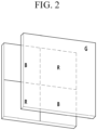
- FIG. 2 is a schematic top plan view of a CMOS image sensor according to at least one example embodiment
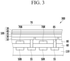
- FIG. 3 is a cross-sectional view of the CMOS image sensor of FIG. 2 .
- a CMOS image sensor 300 includes a semiconductor substrate 110 integrated with a blue photo-sensing device 50B, a red photo-sensing device 50R, a transmission transistor (not shown), and a charge storage 55, a lower insulation layer 60, a color filter layer 70, an upper insulation layer 80, and the photoelectronic device 100.
- the semiconductor substrate 110 may be or include a silicon substrate, and may be integrated with the blue photo-sensing device 50B, the red photo-sensing device 50R, the transmission transistor (not shown), and the charge storage 55.
- the blue photo-sensing device 50B and the red photo-sensing device 50R may be or include photodiodes.
- the blue photo-sensing device 50B, the red photo-sensing device 50R, the transmission transistor, and/or the charge storage 55 may be integrated in each pixel, and as shown in the drawing, the blue photo-sensing device 50B may be included in a blue pixel and the red photo-sensing device 50R may be included in a red pixel.
- the charge storage 55 is shown in only the green pixel, but the blue pixel and red pixel may also each include a charge storage connected with the blue photo-sensing device 50B and a charge storage connected with the red photo-sensing device 50R.
- the blue photo-sensing device 50B and the red photo-sensing device 50R may be configured to sense light, the information sensed by the photo-sensing devices 50B and 50R may be transferred by the transmission transistor, the charge storage 55 of the green pixel may be electrically connected with the photoelectronic device 100 that will be described below, and the information of the charge storage 55 may be transferred by the transmission transistor.
- a metal wire (not shown) and a pad (not shown) may be on the semiconductor substrate 110.
- the metal wire and pad may be made of or include a metal having low resistivity, for example, aluminum (Al), copper (Cu), silver (Ag), and alloys thereof, but is not limited thereto.
- the metal wire and pad are not limited to the illustrated structure, and the metal wire and pad may be under the photo-sensing devices 50B and 50R.
- the lower insulation layer 60 may be formed on the metal wire and the pad.
- the lower insulation layer 60 may be made of or include an inorganic insulating material such as a silicon oxide and/or a silicon nitride, or a low dielectric constant (low K) material such as SiC, SiCOH, SiCO, and SiOF.
- the lower insulation layer 60 may have a trench exposing the charge storage 55. The trench may be filled with fillers.
- a color filter layer 70 may be on the lower insulation layer 60.
- the color filter layer 70 may include a blue filter 70B in the blue pixel and a red filter 70R in the red pixel.
- a green filter is not included, but a green filter may be further included.
- the upper insulation layer 80 may be on the color filter layer 70.
- the upper insulation layer 80 may eliminate a step caused by the color filter layer 70 and may smoothen the surface.
- the upper insulation layer 80 and lower insulation layer 60 may include a contact hole (not shown) exposing a pad, and a through-hole 85 exposing the charge storage 55 of a green pixel.
- the photoelectronic device 100 may be on the upper insulation layer 80.
- the photoelectronic device 100 may include the first electrode 10, the light-absorption layer 30, the light-absorption auxiliary layer 35, the charge auxiliary layer 40, and the second electrode 20 as described above.
- the first electrode 10 and the second electrode 20 may be transparent electrodes, and the light-absorption layer 30, the light-absorption auxiliary layer 35, and the charge auxiliary layer 40 may be as described above.
- the light-absorption layer 30 and light-absorption auxiliary layer 35 are configured to selectively absorb light in a green wavelength region and replace a color filter of a green pixel.
- the light in a green wavelength region may be mainly absorbed in the light-absorption layer 30 and the light-absorption auxiliary layer 35 and photoelectrically converted, while the light in the rest of the wavelength regions passes through the first electrode 10 and may be sensed in the photo-sensing devices 50B and 50R.
- the photoelectronic device that is configured to selectively absorb the light of the green wavelength region is stacked, and thus an image sensor may be down-sized.
- the photoelectronic device 100 may increase green wavelength selectivity due to the light-absorption auxiliary layer 35, and may thus decrease crosstalk that is typically generated by absorbing light except in the green wavelength regions, and increase sensitivity.
- FIG. 4 is a schematic cross-sectional view of a CMOS image sensor according to another example embodiment.
- a CMOS image sensor 300 includes a semiconductor substrate 110 integrated with photo-sensing devices 50B and 50R, a transmission transistor (not shown), a charge storage 55, an insulation layer 80, and a photoelectronic device 100, similarly to the above example embodiment illustrated in Fig. 3 .
- the blue photo-sensing device 50B and the red photo-sensing device 50R are stacked in a vertical direction and the color filter layer 70 may be omitted, unlike in the above example embodiment.
- the blue photo-sensing device 50B and the red photo-sensing device 50R are electrically connected with a charge storage (not shown), and the information sensed by the photo-sensing device may be transferred by a transmission transistor.
- the blue photo-sensing device 50B and the red photo-sensing device 50R may be configured to selectively absorb light in each wavelength region depending on a stacking depth.
- the photoelectronic device that is configured to selectively absorb the light of the green wavelength region is stacked and the red photo-sensing device and the blue photo-sensing device are stacked, and thus an image sensor may be further down-sized.
- the photoelectronic device 100 may increase green wavelength selectivity due to the light-absorption auxiliary layer 35, and thus decrease crosstalk that is generated by absorbing light except in green wavelength region, and increase sensitivity.
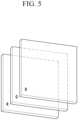
- FIG. 5 is a top plan view schematically showing a CMOS image sensor according to another example embodiment.
- a CMOS image sensor has a structure in which a green photoelectronic device that is configured to selectively absorb light in a green wavelength region, a blue photoelectronic device that is configured to selectively absorb light in a blue wavelength region, and a red photoelectronic device that is configured to selectively absorb light in a red wavelength region are stacked.
- the red photoelectronic device, the green photoelectronic device, and the blue photoelectronic device are sequentially stacked, but the example embodiments are not limited thereto, and the red, green, and blue photoelectronic devices may be stacked in various orders.
- the green photoelectronic device may be the above photoelectronic device 100, the blue photoelectronic device may include electrodes facing each other, a light-absorption layer interposed therebetween, and including an organic material configured to selectively absorb light in a blue wavelength region, and the red photoelectronic device may include electrodes facing each other and a light-absorption layer interposed therebetween and including an organic material configured to selectively absorb light in a red wavelength region.
- a photoelectronic device configured to selectively absorb light in a red wavelength region, a photoelectronic device configured to selectively absorb light in a green wavelength region, and a photoelectronic device configured to selectively absorb light in a blue wavelength region are stacked, and thus may further down-size an image sensor and simultaneously increase sensitivity and decrease crosstalk.
- the image sensor may be applied to various electronic devices, for example a mobile phone, a digital camera, and the like, without limitation.
- ITO is sputtered on a glass substrate to form an approximately 100 nm-thick lower electrode.
- MoOx, 0 ⁇ x ⁇ 3 molybdenum oxide
- Al aluminum
- ETL electron transport layer
- a compound represented by the following Chemical Formula 1a (LumTec, LLC) as a p-type light-absorption material, and dicyanovinyl-terthiophene (DCV3T) as a n-type light-absorption material, are co-deposited in a thickness ratio of 1:1, forming a light-absorption layer.
- a compound represented by the following Chemical Formula 1a is thermally deposited to form a light-absorption auxiliary layer, and a molybdenum oxide (MoOx, 0 ⁇ x ⁇ 3) is thermally deposited thereon, forming a charge auxiliary layer.
- ITO is sputtered to form a 100 nm-thick upper electrode, manufacturing a photoelectronic device.
- a photoelectronic device is manufactured according to the same method as Example 1, except for using fullerene (C60) instead of the dicyanovinyl-terthiophene (DCV3T) as the n-type light-absorption material.
- fullerene C60
- DCV3T dicyanovinyl-terthiophene
- a photoelectronic device is manufactured according to the same method as Example 1, except for using fullerene (C60) instead of the dicyanovinyl-terthiophene (DCV3T) as the n-type light-absorption material of the light-absorption layer, and a compound represented by the following Chemical Formula 1b instead of the compound represented by the above Chemical Formula 1a for the light-absorption auxiliary layer.
- C60 fullerene
- DCV3T dicyanovinyl-terthiophene
- the compound represented by the above Chemical Formula 1b is synthesized by the following method.
- a photoelectronic device is manufactured according to the same method as Example 1, but the photoelectronic device does not have a light-absorption auxiliary layer.
- a photoelectronic device is manufactured according to the same method as Example 2, but the photoelectronic device does not have a light-absorption auxiliary layer.
- a photoelectronic device is manufactured according to the same method as Example 3, but the photoelectronic device does not have a light-absorption auxiliary layer.
- the external quantum efficiency is measured by using an IPCE measurement system.
- the measurement system is calibrated by using a Si photodiode and mounted on the photoelectronic devices according to Examples 1 to 3 and Comparative Examples 1 to 3, and their external quantum efficiency is measured in a wavelength range of about 350 to 750 nm.
- the FWHM is calculated as width of a wavelength corresponding to a half of maximum external quantum efficiency (EQE max ) in the external quantum efficiency (EQE) graph.
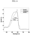
- FIG. 6 is a graph showing external quantum efficiency (EQE) of the photoelectronic devices according to Example 1 and Comparative Example 1 depending on a wavelength
- FIG. 7 is a graph showing external quantum efficiency (EQE) of the photoelectronic devices according to Example 2 and Comparative Example 2 depending on a wavelength
- FIG. 8 is a graph showing external quantum efficiency (EQE) of the photoelectronic devices according to Example 3 and Comparative Example 3 depending on a wavelength.
- the photoelectronic device according to Example 1 shows equivalent or improved external quantum efficiency and narrowed FWHM, and thus improved wavelength selectivity compared with the photoelectronic device according to Comparative Example 1.
- the photoelectronic device according to Example 2 shows equivalent or improved external quantum efficiency and narrowed FWHM, and thus improved wavelength selectivity compared with the photoelectronic device according to Comparative Example 2
- the photoelectronic device according to Example 3 shows equivalent or improved external quantum efficiency and narrowed FWHM, and thus improved wavelength selectivity compared with the photoelectronic device according to Comparative Example 3.
- the crosstalk evaluation is performed through simulation by using a LUMERICAL 3D program.
- a wavelength region is divided into three regions of about 440 to 480 nm (blue), about 520 to 560 nm (green), and about 590 to 630 nm (red), and the optical interference between two other photoelectric transformation elements of different colors in each region is evaluated.
- an integral of a sensitivity curve of a blue element in the blue region of about 440 to 480 nm is regarded as 100
- a relative integral of the sensitivity curves of red and green elements in the blue region of about 440 to 480 nm is calculated.
- the obtained value is a crosstalk of the red and green elements regarding the blue region of about 440 to 480 nm.
- the photoelectronic device according to Example 1 shows greater than or equal to approximately 20 % decreased average crosstalk compared with the photoelectronic device according to Comparative Example 1.
Landscapes
- Physics & Mathematics (AREA)
- Electromagnetism (AREA)
- Chemical & Material Sciences (AREA)
- Engineering & Computer Science (AREA)
- Materials Engineering (AREA)
- Optics & Photonics (AREA)
- Organic Chemistry (AREA)
- Light Receiving Elements (AREA)
- Solid State Image Pick-Up Elements (AREA)
- Electroluminescent Light Sources (AREA)
Claims (11)
- Bildsensor (300), umfassend:eine photoelektronische Vorrichtung (100),wobei die photoelektrische Vorrichtung (100) Folgendes umfasst:eine erste Elektrode (10);eine Lichtabsorptionsschicht (30) auf der ersten Elektrode (10), und die ein erstes Lichtabsorptionsmaterial vom p-Typ und ein erstes Lichtabsorptionsmaterial vom n-Typ beinhaltet;eine Lichtabsorptionshilfsschicht (35) auf der Lichtabsorptionsschicht (30), die ein zweites Lichtabsorptionsmaterial vom p-Typ oder ein zweites Lichtabsorptionsmaterial vom n-Typ beinhaltet;eine Ladungshilfsschicht (40) auf der Lichtabsorptionshilfsschicht (35); undeine zweite Elektrode (20) auf der Ladungshilfsschicht (40), wobeidie Lichtabsorptionsschicht (30) und die Lichtabsorptionshilfsschicht (35) in Kontakt miteinander sind,die Lichtabsorptionsschicht (30) und die Lichtabsorptionshilfsschicht (35) konfiguriert sind, um Licht in einem grünen Wellenlängenbereich selektiv zu absorbieren, dadurch gekennzeichnet, dass das zweite Lichtabsorptionsmaterial vom p-Typ oder das zweite Lichtabsorptionsmaterial vom n-Typ eine kleinere Halbwertsbreite (FWHM) als die Lichtabsorptionsschicht in dem grünen Wellenlängenbereich aufweist;die Ladungshilfsschicht (40) konfiguriert ist, um zu ermöglichen, dass Löcher und Elektronen, die in der Lichtabsorptionsschicht (30) getrennt sind, zu der zweiten Elektrode (20) übertragen werden;die Ladungshilfsschicht (40) konfiguriert ist, um Licht in einem sichtbaren Wellenlängenbereich nicht wesentlich zu absorbieren,wobei jede von der ersten Elektrode (10) und der zweiten Elektrode (20) eine lichtdurchlässige Elektrode ist, unddie zweite Elektrode (20) auf einer Seite ist, von der Licht einfällt.
- Bildsensor nach Anspruch 1, wobei eine externe Quanteneffizienz (EQE) des zweiten Lichtabsorptionsmaterials vom p-Typ oder des zweiten Lichtabsorptionsmaterials vom n-Typ bei einer maximalen Absorptionswellenlänge (λmax) gleich einer oder höher als eine externe Quanteneffizienz (EQE) der Lichtabsorptionsschicht bei einer maximalen Absorptionswellenlänge (λmax) ist.
- Bildsensor nach Anspruch 1 oder 2, wobei eine FWHM der Lichtabsorptionsschicht (30) breiter als eine FWHM des ersten Lichtabsorptionsmaterials vom p-Typ oder des ersten Lichtabsorptionsmaterials vom n-Typ ist.
- Bildsensor nach einem der Ansprüche 1-3, wobei das zweite Lichtabsorptionsmaterial vom p-Typ das gleiche wie das erste Lichtabsorptionsmaterial vom p-Typ ist, und
das zweite Lichtabsorptionsmaterial vom n-Typ das gleiche wie das erste Lichtabsorptionsmaterial vom n-Typ ist. - Bildsensor nach einem der Ansprüche 1-3, wobei sich das zweite Lichtabsorptionsmaterial vom p-Typ von dem ersten Lichtabsorptionsmaterial vom p-Typ unterscheidet, und
sich das zweite Lichtabsorptionsmaterial vom n-Typ von dem ersten Lichtabsorptionsmaterial vom n-Typ unterscheidet. - Bildsensor nach einem der Ansprüche 1-5, wobei das zweite Lichtabsorptionsmaterial vom p-Typ oder das zweite Lichtabsorptionsmaterial vom n-Typ durch die folgende chemische Formel 1 dargestellt ist:
 Ra bis Rl unabhängig Wasserstoff, eine substituierte oder unsubstituierte C1- bis C30-Alkylgruppe, eine substituierte oder unsubstituierte C6- bis C30-Arylgruppe, eine substituierte oder unsubstituierte C3- bis C30-Heteroarylgruppe, ein Halogenatom, eine halogenhaltige Gruppe oder eine Kombination davon sind, undX ein Halogenatom, eine halogenhaltige Gruppe, eine substituierte oder unsubstituierte C1- bis C30-Alkylgruppe, eine substituierte oder unsubstituierte C6- bis C30-Arylgruppe, eine substituierte oder unsubstituierte C1- bis C30-Alkoxygruppe, eine substituierte oder unsubstituierte C1- bis C30-Aryloxygruppe, eine substituierte oder unsubstituierte C1- bis C30-Heteroaryloxygruppe, eine substituierte oder unsubstituierte Silyloxygruppe, eine substituierte oder unsubstituierte Amingruppe, eine substituierte oder unsubstituierte Arylamingruppe oder eine Kombination davon ist.
 - Bildsensor nach einem der Ansprüche 1-5, wobei das erste Lichtabsorptionsmaterial vom p-Typ oder das erste Lichtabsorptionsmaterial vom n-Typ durch die folgende chemische Formel 2 dargestellt ist:
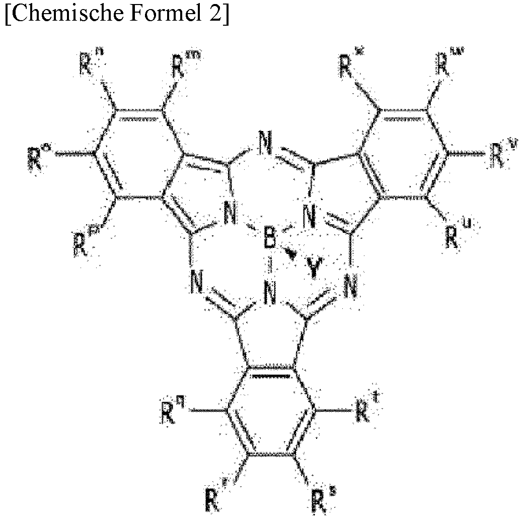 Rm bis Rx unabhängig Wasserstoff, eine substituierte oder unsubstituierte C1- bis C30-Alkylgruppe, eine substituierte oder unsubstituierte C6- bis C30-Arylgruppe, eine substituierte oder unsubstituierte C3- bis C30-Heteroarylgruppe, ein Halogenatom, eine halogenhaltige Gruppe oder eine Kombination davon sind, undY ein Halogenatom ist.
 - Bildsensor nach einem der Ansprüche 1-7, wobei der Bildsensor (300) auf einem Halbleitersubstrat (110) bereitgestellt ist, das mit einer Vielzahl von ersten lichtempfindlichen Vorrichtungen, die Licht in einem blauen Wellenlängenbereich (50B) erfassen, und einer Vielzahl von zweiten lichtempfindlichen Vorrichtungen integriert ist, die Licht in einem roten Wellenlängenbereich (50R) erfassen.
- Bildsensor nach Anspruch 8, ferner umfassend eine Farbfilterschicht (70), die einen Blaufilter, der konfiguriert ist, um Licht in einem blauen Wellenlängenbereich selektiv zu absorbieren, und einen Rotfilter beinhaltet, der konfiguriert ist, um Licht in einem roten Wellenlängenbereich selektiv zu absorbieren, und wobei die Farbfilterschicht zwischen dem Halbleitersubstrat (110) und der photoelektronischen Vorrichtung (100) ist.
- Bildsensor nach einem der Ansprüche 1-9, wobei in der photoelektronischen Vorrichtung (100) eine blaue photoelektronische Vorrichtung, die konfiguriert ist, um Licht in einem blauen Wellenlängenbereich (50B) selektiv zu absorbieren, und eine rote photoelektronische Vorrichtung, die konfiguriert ist, um Licht in einem roten Wellenlängenbereich (50R) selektiv zu absorbieren, gestapelt sind.
- Elektronische Vorrichtung, beinhaltend den Bildsensor (300) nach einem der Ansprüche 1-10.
Applications Claiming Priority (1)
| Application Number | Priority Date | Filing Date | Title |
|---|---|---|---|
| KR1020140089914A KR102243553B1 (ko) | 2014-07-16 | 2014-07-16 | 유기 광전 소자 및 이미지 센서 |
Publications (3)
| Publication Number | Publication Date |
|---|---|
| EP2978023A2 EP2978023A2 (de) | 2016-01-27 |
| EP2978023A3 EP2978023A3 (de) | 2016-02-24 |
| EP2978023B1 true EP2978023B1 (de) | 2023-04-19 |
Family
ID=52391884
Family Applications (1)
| Application Number | Title | Priority Date | Filing Date |
|---|---|---|---|
| EP15152529.2A Active EP2978023B1 (de) | 2014-07-16 | 2015-01-26 | Photoelektronisches Bildsensor |
Country Status (5)
| Country | Link |
|---|---|
| US (2) | US9673259B2 (de) |
| EP (1) | EP2978023B1 (de) |
| JP (4) | JP2016025342A (de) |
| KR (1) | KR102243553B1 (de) |
| CN (1) | CN105261702B (de) |
Families Citing this family (20)
| Publication number | Priority date | Publication date | Assignee | Title |
|---|---|---|---|---|
| JP6479407B2 (ja) * | 2014-10-20 | 2019-03-06 | 株式会社ニューフレアテクノロジー | 放射温度計及び温度測定方法 |
| US10367153B2 (en) * | 2015-02-12 | 2019-07-30 | Sony Semiconductor Solutions Corporation | Photoelectric conversion film, solid state imaging element, and electronic device |
| KR102491494B1 (ko) | 2015-09-25 | 2023-01-20 | 삼성전자주식회사 | 유기 광전 소자용 화합물 및 이를 포함하는 유기 광전 소자 및 이미지 센서 |
| KR102547655B1 (ko) * | 2015-11-18 | 2023-06-23 | 삼성전자주식회사 | 이미지 센서 및 이를 포함하는 전자 장치 |
| KR102529631B1 (ko) | 2015-11-30 | 2023-05-04 | 삼성전자주식회사 | 유기 광전 소자 및 이미지 센서 |
| EP3414786A1 (de) * | 2016-02-12 | 2018-12-19 | SABIC Global Technologies B.V. | Lichtempfindliches laminat, verfahren zur herstellung und bildsensorvorrichtungen |
| KR102557864B1 (ko) | 2016-04-06 | 2023-07-19 | 삼성전자주식회사 | 화합물, 및 이를 포함하는 유기 광전 소자, 이미지 센서 및 전자 장치 |
| US10236461B2 (en) | 2016-05-20 | 2019-03-19 | Samsung Electronics Co., Ltd. | Organic photoelectronic device and image sensor |
| KR102605375B1 (ko) | 2016-06-29 | 2023-11-22 | 삼성전자주식회사 | 유기 광전 소자 및 이미지 센서 |
| CN116744702A (zh) * | 2016-07-20 | 2023-09-12 | 索尼公司 | 光检测元件和光检测装置 |
| KR102589215B1 (ko) | 2016-08-29 | 2023-10-12 | 삼성전자주식회사 | 유기 광전 소자, 이미지 센서 및 전자 장치 |
| KR102285797B1 (ko) * | 2017-09-05 | 2021-08-03 | 삼성전자주식회사 | 유기 광전 소자, 이미지 센서 및 전자 장치 |
| KR102298231B1 (ko) * | 2017-10-19 | 2021-09-07 | 엘티소재주식회사 | 헤테로고리 화합물 및 이를 이용한 유기 발광 소자 |
| US11145822B2 (en) | 2017-10-20 | 2021-10-12 | Samsung Electronics Co., Ltd. | Compound and photoelectric device, image sensor, and electronic device including the same |
| US10998514B2 (en) * | 2017-12-01 | 2021-05-04 | Samsung Electronics Co., Ltd. | Photoelectric devices and image sensors and electronic devices |
| CN109141632A (zh) * | 2018-11-06 | 2019-01-04 | 德淮半导体有限公司 | 像素单元、图像传感器及其制造方法以及成像装置 |
| KR102736230B1 (ko) * | 2019-05-17 | 2024-11-28 | 삼성전자주식회사 | 광전 변환 소자, 유기 센서 및 전자 장치 |
| KR102763275B1 (ko) * | 2019-07-15 | 2025-02-10 | 삼성디스플레이 주식회사 | 화합물 및 이를 포함하는 유기 발광 소자 |
| KR102764010B1 (ko) * | 2020-04-29 | 2025-02-05 | 삼성전자주식회사 | 센서 및 전자 장치 |
| KR20220161052A (ko) | 2021-05-28 | 2022-12-06 | 삼성전자주식회사 | 센서 내장형 표시 패널 및 전자 장치 |
Citations (1)
| Publication number | Priority date | Publication date | Assignee | Title |
|---|---|---|---|---|
| WO2014085639A1 (en) * | 2012-11-28 | 2014-06-05 | The Regents Of The University Of Michigan | Hybrid planar-graded heterojunction for organic photovoltaics |
Family Cites Families (35)
| Publication number | Priority date | Publication date | Assignee | Title |
|---|---|---|---|---|
| JP4817584B2 (ja) | 2002-05-08 | 2011-11-16 | キヤノン株式会社 | カラー撮像素子 |
| US7570292B2 (en) * | 2004-03-19 | 2009-08-04 | Fujifilm Corporation | Photoelectric conversion film, photoelectric conversion element, imaging element, method of applying electric field thereto and electric field-applied element |
| US7326955B2 (en) * | 2004-08-05 | 2008-02-05 | The Trustees Of Princeton University | Stacked organic photosensitive devices |
| DE102005010978A1 (de) * | 2005-03-04 | 2006-09-07 | Technische Universität Dresden | Photoaktives Bauelement mit organischen Schichten |
| DE102005010979A1 (de) | 2005-03-04 | 2006-09-21 | Technische Universität Dresden | Photoaktives Bauelement mit organischen Schichten |
| KR20070113077A (ko) * | 2006-05-23 | 2007-11-28 | 제일모직주식회사 | 광학필름, 그를 포함하는 광학필터 및 디스플레이 장치 |
| US7655306B2 (en) | 2006-05-23 | 2010-02-02 | Cheil Industries, Inc. | Optical film, optical filter and display device including the same |
| US20070272918A1 (en) | 2006-05-25 | 2007-11-29 | Barry Rand | Organic photosensitive devices using subphthalocyanine compounds |
| US7955889B1 (en) | 2006-07-11 | 2011-06-07 | The Trustees Of Princeton University | Organic photosensitive cells grown on rough electrode with nano-scale morphology control |
| JP2008103670A (ja) * | 2006-09-22 | 2008-05-01 | Nissan Motor Co Ltd | 有機薄膜受光素子、有機薄膜受光素子の製造方法、有機薄膜受発光素子、有機薄膜受発光素子の製造方法、及び脈拍センサ |
| JP5172175B2 (ja) * | 2007-02-28 | 2013-03-27 | 富士フイルム株式会社 | 光電変換素子及び固体撮像素子 |
| KR100947451B1 (ko) * | 2007-03-09 | 2010-03-11 | 삼성코닝정밀유리 주식회사 | 광학 부재 및 이를 포함하는 디스플레이 장치용 필터 |
| JP2009049278A (ja) * | 2007-08-22 | 2009-03-05 | Fujifilm Corp | 光電変換素子、光電変換素子の製造方法、固体撮像素子 |
| KR101447113B1 (ko) * | 2008-01-15 | 2014-10-07 | 삼성전자주식회사 | 화합물 반도체 수직 적층 이미지 센서 |
| JP5258037B2 (ja) * | 2008-09-08 | 2013-08-07 | 国立大学法人京都大学 | 光電変換素子、その製造方法、及び太陽電池 |
| KR20160142888A (ko) | 2008-10-27 | 2016-12-13 | 더 리젠츠 오브 더 유니버시티 오브 미시간 | 역전 유기 감광성 디바이스 |
| JP2010141140A (ja) * | 2008-12-11 | 2010-06-24 | Nippon Hoso Kyokai <Nhk> | カラーイメージセンサ |
| JP5444743B2 (ja) | 2009-02-03 | 2014-03-19 | コニカミノルタ株式会社 | 有機光電変換素子 |
| KR101034466B1 (ko) | 2009-02-09 | 2011-05-17 | 한국과학기술연구원 | 정공이동도가 우수한 유기박막층을 이용하여 증가된 효율을갖는 유기 광전 변환 소자 및 그의 제조방법 |
| JP5488595B2 (ja) | 2009-05-22 | 2014-05-14 | コニカミノルタ株式会社 | 有機光電変換素子 |
| JP2011054869A (ja) * | 2009-09-04 | 2011-03-17 | Nippon Hoso Kyokai <Nhk> | 有機光電変換素子、及び、これを含むイメージセンサ |
| US20120216870A1 (en) | 2009-11-03 | 2012-08-30 | University Of Florida Research Foundation Inc. | Interlayer for organic solar cells |
| JP2011204802A (ja) * | 2010-03-24 | 2011-10-13 | Fujifilm Corp | 有機光電変換素子、撮像素子、撮像装置 |
| JP5464088B2 (ja) | 2010-07-26 | 2014-04-09 | コニカミノルタ株式会社 | 有機光電変換素子、太陽電池及び光センサアレイ |
| US11211559B2 (en) * | 2010-10-15 | 2021-12-28 | The Regents Of The University Of Michigan | Materials for controlling the epitaxial growth of photoactive layers in photovoltaic devices |
| EP2742112B1 (de) * | 2011-08-12 | 2016-05-18 | Basf Se | Carbazolocarbazol-bis(dicarboximide) und ihre verwendung als halbleiter |
| JP2012191222A (ja) * | 2012-05-21 | 2012-10-04 | Fujifilm Corp | 光電変換素子の製造方法 |
| JP2012231149A (ja) * | 2012-06-05 | 2012-11-22 | Mitsubishi Chemicals Corp | 有機光電変換素子の製造方法及び有機光電変換素子 |
| US9508945B2 (en) * | 2012-06-27 | 2016-11-29 | Regents Of The University Of Minnesota | Spectrally tunable broadband organic photodetectors |
| JP5969843B2 (ja) * | 2012-07-17 | 2016-08-17 | 日本放送協会 | 有機光電変換素子、及び、これを含む受光素子 |
| US9379343B2 (en) | 2012-09-10 | 2016-06-28 | Samsung Electronics Co., Ltd. | Light transmissive electrode, organic photoelectric device, and image sensor |
| KR101960468B1 (ko) * | 2012-10-08 | 2019-03-21 | 삼성전자주식회사 | 유기 광전 소자 및 이미지 센서 |
| EP2923389B1 (de) * | 2012-11-22 | 2021-08-11 | The Regents Of The University Of Michigan | Hybrider, planarer, gemischter heteroübergang für organische photovoltaik |
| JP6135109B2 (ja) | 2012-12-07 | 2017-05-31 | ソニー株式会社 | 固体撮像素子および固体撮像素子の製造方法ならびに電子機器 |
| JP6185431B2 (ja) * | 2014-06-23 | 2017-08-23 | ソニーセミコンダクタソリューションズ株式会社 | 光電変換膜、固体撮像素子、および電子機器 |
-
2014
- 2014-07-16 KR KR1020140089914A patent/KR102243553B1/ko active Active
-
2015
- 2015-01-23 US US14/604,185 patent/US9673259B2/en active Active
- 2015-01-26 EP EP15152529.2A patent/EP2978023B1/de active Active
- 2015-02-10 JP JP2015024570A patent/JP2016025342A/ja active Pending
- 2015-03-19 CN CN201510122544.XA patent/CN105261702B/zh active Active
-
2017
- 2017-05-12 US US15/593,631 patent/US10141376B2/en active Active
-
2019
- 2019-11-29 JP JP2019217095A patent/JP2020039000A/ja active Pending
-
2021
- 2021-11-08 JP JP2021182155A patent/JP7214817B2/ja active Active
-
2023
- 2023-01-18 JP JP2023006043A patent/JP7554855B2/ja active Active
Patent Citations (1)
| Publication number | Priority date | Publication date | Assignee | Title |
|---|---|---|---|---|
| WO2014085639A1 (en) * | 2012-11-28 | 2014-06-05 | The Regents Of The University Of Michigan | Hybrid planar-graded heterojunction for organic photovoltaics |
Also Published As
| Publication number | Publication date |
|---|---|
| US9673259B2 (en) | 2017-06-06 |
| US20170250227A1 (en) | 2017-08-31 |
| KR20160009404A (ko) | 2016-01-26 |
| JP2020039000A (ja) | 2020-03-12 |
| CN105261702B (zh) | 2019-04-16 |
| JP2016025342A (ja) | 2016-02-08 |
| US20160020258A1 (en) | 2016-01-21 |
| EP2978023A3 (de) | 2016-02-24 |
| KR102243553B1 (ko) | 2021-04-22 |
| CN105261702A (zh) | 2016-01-20 |
| EP2978023A2 (de) | 2016-01-27 |
| US10141376B2 (en) | 2018-11-27 |
| JP7554855B2 (ja) | 2024-09-20 |
| JP2023066421A (ja) | 2023-05-15 |
| JP2022019767A (ja) | 2022-01-27 |
| JP7214817B2 (ja) | 2023-01-30 |
Similar Documents
| Publication | Publication Date | Title |
|---|---|---|
| EP2978023B1 (de) | Photoelektronisches Bildsensor | |
| CN103524531B (zh) | 有机光电材料和有机光电器件以及图像传感器 | |
| US10256414B2 (en) | Organic photoelectronic device and image sensor | |
| US9666810B2 (en) | Organic photoelectric device, and image sensor and electronic device including the same | |
| US9911920B2 (en) | Compound, organic photoelectronic device and image sensor | |
| US9520571B2 (en) | Organic photoelectric device and image sensor | |
| KR102314129B1 (ko) | 유기 광전 소자 및 이미지 센서 | |
| US10636844B2 (en) | Organic photoelectronic device and image sensor including selective light transmittance layer | |
| US9548336B2 (en) | Image sensors and electronic devices including the same | |
| US10263042B2 (en) | Organic photoelectric device and image sensor | |
| US9831436B2 (en) | Organic photoelectronic device and image sensor | |
| US9786847B2 (en) | Compound for organic photoelectric device, and organic photoelectric device and image sensor including the same | |
| US9130175B2 (en) | Organic photoelectric device and image sensor each having active layer including quinacridone and subPC compounds | |
| US9368727B2 (en) | Organic photoelectric device and image sensor including the same | |
| US9608212B2 (en) | Organic photoelectric devices, image sensors, and electronic devices | |
| EP2975644B1 (de) | Verbindung, organische fotoelektronische vorrichtung und bildsensor |
Legal Events
| Date | Code | Title | Description |
|---|---|---|---|
| PUAL | Search report despatched |
Free format text: ORIGINAL CODE: 0009013 |
|
| PUAI | Public reference made under article 153(3) epc to a published international application that has entered the european phase |
Free format text: ORIGINAL CODE: 0009012 |
|
| AK | Designated contracting states |
Kind code of ref document: A2 Designated state(s): AL AT BE BG CH CY CZ DE DK EE ES FI FR GB GR HR HU IE IS IT LI LT LU LV MC MK MT NL NO PL PT RO RS SE SI SK SM TR |
|
| AX | Request for extension of the european patent |
Extension state: BA ME |
|
| AK | Designated contracting states |
Kind code of ref document: A3 Designated state(s): AL AT BE BG CH CY CZ DE DK EE ES FI FR GB GR HR HU IE IS IT LI LT LU LV MC MK MT NL NO PL PT RO RS SE SI SK SM TR |
|
| AX | Request for extension of the european patent |
Extension state: BA ME |
|
| RIC1 | Information provided on ipc code assigned before grant |
Ipc: H01L 27/30 20060101AFI20160120BHEP Ipc: H01L 51/00 20060101ALI20160120BHEP Ipc: C09B 47/04 20060101ALI20160120BHEP Ipc: H01L 51/42 20060101ALI20160120BHEP |
|
| 17P | Request for examination filed |
Effective date: 20160824 |
|
| RBV | Designated contracting states (corrected) |
Designated state(s): AL AT BE BG CH CY CZ DE DK EE ES FI FR GB GR HR HU IE IS IT LI LT LU LV MC MK MT NL NO PL PT RO RS SE SI SK SM TR |
|
| STAA | Information on the status of an ep patent application or granted ep patent |
Free format text: STATUS: EXAMINATION IS IN PROGRESS |
|
| 17Q | First examination report despatched |
Effective date: 20190423 |
|
| GRAP | Despatch of communication of intention to grant a patent |
Free format text: ORIGINAL CODE: EPIDOSNIGR1 |
|
| STAA | Information on the status of an ep patent application or granted ep patent |
Free format text: STATUS: GRANT OF PATENT IS INTENDED |
|
| INTG | Intention to grant announced |
Effective date: 20221201 |
|
| GRAS | Grant fee paid |
Free format text: ORIGINAL CODE: EPIDOSNIGR3 |
|
| GRAA | (expected) grant |
Free format text: ORIGINAL CODE: 0009210 |
|
| STAA | Information on the status of an ep patent application or granted ep patent |
Free format text: STATUS: THE PATENT HAS BEEN GRANTED |
|
| AK | Designated contracting states |
Kind code of ref document: B1 Designated state(s): AL AT BE BG CH CY CZ DE DK EE ES FI FR GB GR HR HU IE IS IT LI LT LU LV MC MK MT NL NO PL PT RO RS SE SI SK SM TR |
|
| REG | Reference to a national code |
Ref country code: GB Ref legal event code: FG4D |
|
| REG | Reference to a national code |
Ref country code: CH Ref legal event code: EP |
|
| REG | Reference to a national code |
Ref country code: DE Ref legal event code: R096 Ref document number: 602015083196 Country of ref document: DE |
|
| REG | Reference to a national code |
Ref country code: IE Ref legal event code: FG4D |
|
| REG | Reference to a national code |
Ref country code: AT Ref legal event code: REF Ref document number: 1561834 Country of ref document: AT Kind code of ref document: T Effective date: 20230515 |
|
| P01 | Opt-out of the competence of the unified patent court (upc) registered |
Effective date: 20230519 |
|
| REG | Reference to a national code |
Ref country code: LT Ref legal event code: MG9D |
|
| REG | Reference to a national code |
Ref country code: NL Ref legal event code: MP Effective date: 20230419 |
|
| REG | Reference to a national code |
Ref country code: AT Ref legal event code: MK05 Ref document number: 1561834 Country of ref document: AT Kind code of ref document: T Effective date: 20230419 |
|
| PG25 | Lapsed in a contracting state [announced via postgrant information from national office to epo] |
Ref country code: NL Free format text: LAPSE BECAUSE OF FAILURE TO SUBMIT A TRANSLATION OF THE DESCRIPTION OR TO PAY THE FEE WITHIN THE PRESCRIBED TIME-LIMIT Effective date: 20230419 |
|
| PG25 | Lapsed in a contracting state [announced via postgrant information from national office to epo] |
Ref country code: SE Free format text: LAPSE BECAUSE OF FAILURE TO SUBMIT A TRANSLATION OF THE DESCRIPTION OR TO PAY THE FEE WITHIN THE PRESCRIBED TIME-LIMIT Effective date: 20230419 Ref country code: PT Free format text: LAPSE BECAUSE OF FAILURE TO SUBMIT A TRANSLATION OF THE DESCRIPTION OR TO PAY THE FEE WITHIN THE PRESCRIBED TIME-LIMIT Effective date: 20230821 Ref country code: NO Free format text: LAPSE BECAUSE OF FAILURE TO SUBMIT A TRANSLATION OF THE DESCRIPTION OR TO PAY THE FEE WITHIN THE PRESCRIBED TIME-LIMIT Effective date: 20230719 Ref country code: ES Free format text: LAPSE BECAUSE OF FAILURE TO SUBMIT A TRANSLATION OF THE DESCRIPTION OR TO PAY THE FEE WITHIN THE PRESCRIBED TIME-LIMIT Effective date: 20230419 Ref country code: AT Free format text: LAPSE BECAUSE OF FAILURE TO SUBMIT A TRANSLATION OF THE DESCRIPTION OR TO PAY THE FEE WITHIN THE PRESCRIBED TIME-LIMIT Effective date: 20230419 |
|
| PG25 | Lapsed in a contracting state [announced via postgrant information from national office to epo] |
Ref country code: RS Free format text: LAPSE BECAUSE OF FAILURE TO SUBMIT A TRANSLATION OF THE DESCRIPTION OR TO PAY THE FEE WITHIN THE PRESCRIBED TIME-LIMIT Effective date: 20230419 Ref country code: PL Free format text: LAPSE BECAUSE OF FAILURE TO SUBMIT A TRANSLATION OF THE DESCRIPTION OR TO PAY THE FEE WITHIN THE PRESCRIBED TIME-LIMIT Effective date: 20230419 Ref country code: LV Free format text: LAPSE BECAUSE OF FAILURE TO SUBMIT A TRANSLATION OF THE DESCRIPTION OR TO PAY THE FEE WITHIN THE PRESCRIBED TIME-LIMIT Effective date: 20230419 Ref country code: LT Free format text: LAPSE BECAUSE OF FAILURE TO SUBMIT A TRANSLATION OF THE DESCRIPTION OR TO PAY THE FEE WITHIN THE PRESCRIBED TIME-LIMIT Effective date: 20230419 Ref country code: IS Free format text: LAPSE BECAUSE OF FAILURE TO SUBMIT A TRANSLATION OF THE DESCRIPTION OR TO PAY THE FEE WITHIN THE PRESCRIBED TIME-LIMIT Effective date: 20230819 Ref country code: HR Free format text: LAPSE BECAUSE OF FAILURE TO SUBMIT A TRANSLATION OF THE DESCRIPTION OR TO PAY THE FEE WITHIN THE PRESCRIBED TIME-LIMIT Effective date: 20230419 Ref country code: GR Free format text: LAPSE BECAUSE OF FAILURE TO SUBMIT A TRANSLATION OF THE DESCRIPTION OR TO PAY THE FEE WITHIN THE PRESCRIBED TIME-LIMIT Effective date: 20230720 Ref country code: AL Free format text: LAPSE BECAUSE OF FAILURE TO SUBMIT A TRANSLATION OF THE DESCRIPTION OR TO PAY THE FEE WITHIN THE PRESCRIBED TIME-LIMIT Effective date: 20230419 |
|
| PG25 | Lapsed in a contracting state [announced via postgrant information from national office to epo] |
Ref country code: FI Free format text: LAPSE BECAUSE OF FAILURE TO SUBMIT A TRANSLATION OF THE DESCRIPTION OR TO PAY THE FEE WITHIN THE PRESCRIBED TIME-LIMIT Effective date: 20230419 |
|
| PG25 | Lapsed in a contracting state [announced via postgrant information from national office to epo] |
Ref country code: SK Free format text: LAPSE BECAUSE OF FAILURE TO SUBMIT A TRANSLATION OF THE DESCRIPTION OR TO PAY THE FEE WITHIN THE PRESCRIBED TIME-LIMIT Effective date: 20230419 |
|
| REG | Reference to a national code |
Ref country code: DE Ref legal event code: R097 Ref document number: 602015083196 Country of ref document: DE |
|
| PG25 | Lapsed in a contracting state [announced via postgrant information from national office to epo] |
Ref country code: SM Free format text: LAPSE BECAUSE OF FAILURE TO SUBMIT A TRANSLATION OF THE DESCRIPTION OR TO PAY THE FEE WITHIN THE PRESCRIBED TIME-LIMIT Effective date: 20230419 Ref country code: SK Free format text: LAPSE BECAUSE OF FAILURE TO SUBMIT A TRANSLATION OF THE DESCRIPTION OR TO PAY THE FEE WITHIN THE PRESCRIBED TIME-LIMIT Effective date: 20230419 Ref country code: RO Free format text: LAPSE BECAUSE OF FAILURE TO SUBMIT A TRANSLATION OF THE DESCRIPTION OR TO PAY THE FEE WITHIN THE PRESCRIBED TIME-LIMIT Effective date: 20230419 Ref country code: EE Free format text: LAPSE BECAUSE OF FAILURE TO SUBMIT A TRANSLATION OF THE DESCRIPTION OR TO PAY THE FEE WITHIN THE PRESCRIBED TIME-LIMIT Effective date: 20230419 Ref country code: DK Free format text: LAPSE BECAUSE OF FAILURE TO SUBMIT A TRANSLATION OF THE DESCRIPTION OR TO PAY THE FEE WITHIN THE PRESCRIBED TIME-LIMIT Effective date: 20230419 Ref country code: CZ Free format text: LAPSE BECAUSE OF FAILURE TO SUBMIT A TRANSLATION OF THE DESCRIPTION OR TO PAY THE FEE WITHIN THE PRESCRIBED TIME-LIMIT Effective date: 20230419 |
|
| PLBE | No opposition filed within time limit |
Free format text: ORIGINAL CODE: 0009261 |
|
| STAA | Information on the status of an ep patent application or granted ep patent |
Free format text: STATUS: NO OPPOSITION FILED WITHIN TIME LIMIT |
|
| 26N | No opposition filed |
Effective date: 20240122 |
|
| PG25 | Lapsed in a contracting state [announced via postgrant information from national office to epo] |
Ref country code: SI Free format text: LAPSE BECAUSE OF FAILURE TO SUBMIT A TRANSLATION OF THE DESCRIPTION OR TO PAY THE FEE WITHIN THE PRESCRIBED TIME-LIMIT Effective date: 20230419 |
|
| PG25 | Lapsed in a contracting state [announced via postgrant information from national office to epo] |
Ref country code: SI Free format text: LAPSE BECAUSE OF FAILURE TO SUBMIT A TRANSLATION OF THE DESCRIPTION OR TO PAY THE FEE WITHIN THE PRESCRIBED TIME-LIMIT Effective date: 20230419 Ref country code: IT Free format text: LAPSE BECAUSE OF FAILURE TO SUBMIT A TRANSLATION OF THE DESCRIPTION OR TO PAY THE FEE WITHIN THE PRESCRIBED TIME-LIMIT Effective date: 20230419 |
|
| PG25 | Lapsed in a contracting state [announced via postgrant information from national office to epo] |
Ref country code: MC Free format text: LAPSE BECAUSE OF FAILURE TO SUBMIT A TRANSLATION OF THE DESCRIPTION OR TO PAY THE FEE WITHIN THE PRESCRIBED TIME-LIMIT Effective date: 20230419 |
|
| PG25 | Lapsed in a contracting state [announced via postgrant information from national office to epo] |
Ref country code: MC Free format text: LAPSE BECAUSE OF FAILURE TO SUBMIT A TRANSLATION OF THE DESCRIPTION OR TO PAY THE FEE WITHIN THE PRESCRIBED TIME-LIMIT Effective date: 20230419 |
|
| REG | Reference to a national code |
Ref country code: CH Ref legal event code: PL |
|
| PG25 | Lapsed in a contracting state [announced via postgrant information from national office to epo] |
Ref country code: LU Free format text: LAPSE BECAUSE OF NON-PAYMENT OF DUE FEES Effective date: 20240126 |
|
| PG25 | Lapsed in a contracting state [announced via postgrant information from national office to epo] |
Ref country code: LU Free format text: LAPSE BECAUSE OF NON-PAYMENT OF DUE FEES Effective date: 20240126 |
|
| PG25 | Lapsed in a contracting state [announced via postgrant information from national office to epo] |
Ref country code: BE Free format text: LAPSE BECAUSE OF NON-PAYMENT OF DUE FEES Effective date: 20240131 |
|
| PG25 | Lapsed in a contracting state [announced via postgrant information from national office to epo] |
Ref country code: CH Free format text: LAPSE BECAUSE OF NON-PAYMENT OF DUE FEES Effective date: 20240131 |
|
| PG25 | Lapsed in a contracting state [announced via postgrant information from national office to epo] |
Ref country code: CH Free format text: LAPSE BECAUSE OF NON-PAYMENT OF DUE FEES Effective date: 20240131 Ref country code: BE Free format text: LAPSE BECAUSE OF NON-PAYMENT OF DUE FEES Effective date: 20240131 |
|
| REG | Reference to a national code |
Ref country code: BE Ref legal event code: MM Effective date: 20240131 |
|
| PG25 | Lapsed in a contracting state [announced via postgrant information from national office to epo] |
Ref country code: BG Free format text: LAPSE BECAUSE OF FAILURE TO SUBMIT A TRANSLATION OF THE DESCRIPTION OR TO PAY THE FEE WITHIN THE PRESCRIBED TIME-LIMIT Effective date: 20230419 |
|
| PG25 | Lapsed in a contracting state [announced via postgrant information from national office to epo] |
Ref country code: BG Free format text: LAPSE BECAUSE OF FAILURE TO SUBMIT A TRANSLATION OF THE DESCRIPTION OR TO PAY THE FEE WITHIN THE PRESCRIBED TIME-LIMIT Effective date: 20230419 |
|
| PG25 | Lapsed in a contracting state [announced via postgrant information from national office to epo] |
Ref country code: IE Free format text: LAPSE BECAUSE OF NON-PAYMENT OF DUE FEES Effective date: 20240126 |
|
| PG25 | Lapsed in a contracting state [announced via postgrant information from national office to epo] |
Ref country code: IE Free format text: LAPSE BECAUSE OF NON-PAYMENT OF DUE FEES Effective date: 20240126 |
|
| PG25 | Lapsed in a contracting state [announced via postgrant information from national office to epo] |
Ref country code: CY Free format text: LAPSE BECAUSE OF FAILURE TO SUBMIT A TRANSLATION OF THE DESCRIPTION OR TO PAY THE FEE WITHIN THE PRESCRIBED TIME-LIMIT; INVALID AB INITIO Effective date: 20150126 |
|
| PG25 | Lapsed in a contracting state [announced via postgrant information from national office to epo] |
Ref country code: HU Free format text: LAPSE BECAUSE OF FAILURE TO SUBMIT A TRANSLATION OF THE DESCRIPTION OR TO PAY THE FEE WITHIN THE PRESCRIBED TIME-LIMIT; INVALID AB INITIO Effective date: 20150126 |
|
| PG25 | Lapsed in a contracting state [announced via postgrant information from national office to epo] |
Ref country code: TR Free format text: LAPSE BECAUSE OF FAILURE TO SUBMIT A TRANSLATION OF THE DESCRIPTION OR TO PAY THE FEE WITHIN THE PRESCRIBED TIME-LIMIT Effective date: 20230419 |
|
| PGFP | Annual fee paid to national office [announced via postgrant information from national office to epo] |
Ref country code: GB Payment date: 20251211 Year of fee payment: 12 |
|
| PGFP | Annual fee paid to national office [announced via postgrant information from national office to epo] |
Ref country code: FR Payment date: 20251222 Year of fee payment: 12 |
|
| PGFP | Annual fee paid to national office [announced via postgrant information from national office to epo] |
Ref country code: DE Payment date: 20251216 Year of fee payment: 12 |