EP2978076A1 - Connecteur électrique et douille pour composant électrique - Google Patents
Connecteur électrique et douille pour composant électrique Download PDFInfo
- Publication number
- EP2978076A1 EP2978076A1 EP14770603.0A EP14770603A EP2978076A1 EP 2978076 A1 EP2978076 A1 EP 2978076A1 EP 14770603 A EP14770603 A EP 14770603A EP 2978076 A1 EP2978076 A1 EP 2978076A1
- Authority
- EP
- European Patent Office
- Prior art keywords
- layer
- alloy
- electrical connector
- socket
- package
- Prior art date
- Legal status (The legal status is an assumption and is not a legal conclusion. Google has not performed a legal analysis and makes no representation as to the accuracy of the status listed.)
- Granted
Links
Images





Classifications
-
- H—ELECTRICITY
- H01—ELECTRIC ELEMENTS
- H01R—ELECTRICALLY-CONDUCTIVE CONNECTIONS; STRUCTURAL ASSOCIATIONS OF A PLURALITY OF MUTUALLY-INSULATED ELECTRICAL CONNECTING ELEMENTS; COUPLING DEVICES; CURRENT COLLECTORS
- H01R13/00—Details of coupling devices of the kinds covered by groups H01R12/70 or H01R24/00 - H01R33/00
- H01R13/02—Contact members
- H01R13/03—Contact members characterised by the material, e.g. plating, or coating materials
-
- B—PERFORMING OPERATIONS; TRANSPORTING
- B32—LAYERED PRODUCTS
- B32B—LAYERED PRODUCTS, i.e. PRODUCTS BUILT-UP OF STRATA OF FLAT OR NON-FLAT, e.g. CELLULAR OR HONEYCOMB, FORM
- B32B15/00—Layered products comprising a layer of metal
- B32B15/01—Layered products comprising a layer of metal all layers being exclusively metallic
-
- C—CHEMISTRY; METALLURGY
- C22—METALLURGY; FERROUS OR NON-FERROUS ALLOYS; TREATMENT OF ALLOYS OR NON-FERROUS METALS
- C22C—ALLOYS
- C22C5/00—Alloys based on noble metals
- C22C5/04—Alloys based on a platinum group metal
-
- C—CHEMISTRY; METALLURGY
- C22—METALLURGY; FERROUS OR NON-FERROUS ALLOYS; TREATMENT OF ALLOYS OR NON-FERROUS METALS
- C22C—ALLOYS
- C22C5/00—Alloys based on noble metals
- C22C5/06—Alloys based on silver
-
- C—CHEMISTRY; METALLURGY
- C22—METALLURGY; FERROUS OR NON-FERROUS ALLOYS; TREATMENT OF ALLOYS OR NON-FERROUS METALS
- C22C—ALLOYS
- C22C9/00—Alloys based on copper
-
- C—CHEMISTRY; METALLURGY
- C23—COATING METALLIC MATERIAL; COATING MATERIAL WITH METALLIC MATERIAL; CHEMICAL SURFACE TREATMENT; DIFFUSION TREATMENT OF METALLIC MATERIAL; COATING BY VACUUM EVAPORATION, BY SPUTTERING, BY ION IMPLANTATION OR BY CHEMICAL VAPOUR DEPOSITION, IN GENERAL; INHIBITING CORROSION OF METALLIC MATERIAL OR INCRUSTATION IN GENERAL
- C23C—COATING METALLIC MATERIAL; COATING MATERIAL WITH METALLIC MATERIAL; SURFACE TREATMENT OF METALLIC MATERIAL BY DIFFUSION INTO THE SURFACE, BY CHEMICAL CONVERSION OR SUBSTITUTION; COATING BY VACUUM EVAPORATION, BY SPUTTERING, BY ION IMPLANTATION OR BY CHEMICAL VAPOUR DEPOSITION, IN GENERAL
- C23C18/00—Chemical coating by decomposition of either liquid compounds or solutions of the coating forming compounds, without leaving reaction products of surface material in the coating; Contact plating
- C23C18/16—Chemical coating by decomposition of either liquid compounds or solutions of the coating forming compounds, without leaving reaction products of surface material in the coating; Contact plating by reduction or substitution, e.g. electroless plating
- C23C18/1601—Process or apparatus
- C23C18/1633—Process of electroless plating
- C23C18/1646—Characteristics of the product obtained
- C23C18/165—Multilayered product
- C23C18/1651—Two or more layers only obtained by electroless plating
-
- C—CHEMISTRY; METALLURGY
- C23—COATING METALLIC MATERIAL; COATING MATERIAL WITH METALLIC MATERIAL; CHEMICAL SURFACE TREATMENT; DIFFUSION TREATMENT OF METALLIC MATERIAL; COATING BY VACUUM EVAPORATION, BY SPUTTERING, BY ION IMPLANTATION OR BY CHEMICAL VAPOUR DEPOSITION, IN GENERAL; INHIBITING CORROSION OF METALLIC MATERIAL OR INCRUSTATION IN GENERAL
- C23C—COATING METALLIC MATERIAL; COATING MATERIAL WITH METALLIC MATERIAL; SURFACE TREATMENT OF METALLIC MATERIAL BY DIFFUSION INTO THE SURFACE, BY CHEMICAL CONVERSION OR SUBSTITUTION; COATING BY VACUUM EVAPORATION, BY SPUTTERING, BY ION IMPLANTATION OR BY CHEMICAL VAPOUR DEPOSITION, IN GENERAL
- C23C18/00—Chemical coating by decomposition of either liquid compounds or solutions of the coating forming compounds, without leaving reaction products of surface material in the coating; Contact plating
- C23C18/16—Chemical coating by decomposition of either liquid compounds or solutions of the coating forming compounds, without leaving reaction products of surface material in the coating; Contact plating by reduction or substitution, e.g. electroless plating
- C23C18/1601—Process or apparatus
- C23C18/1633—Process of electroless plating
- C23C18/1646—Characteristics of the product obtained
- C23C18/165—Multilayered product
- C23C18/1653—Two or more layers with at least one layer obtained by electroless plating and one layer obtained by electroplating
-
- C—CHEMISTRY; METALLURGY
- C25—ELECTROLYTIC OR ELECTROPHORETIC PROCESSES; APPARATUS THEREFOR
- C25D—PROCESSES FOR THE ELECTROLYTIC OR ELECTROPHORETIC PRODUCTION OF COATINGS; ELECTROFORMING; APPARATUS THEREFOR
- C25D5/00—Electroplating characterised by the process; Pretreatment or after-treatment of workpieces
- C25D5/10—Electroplating with more than one layer of the same or of different metals
-
- C—CHEMISTRY; METALLURGY
- C25—ELECTROLYTIC OR ELECTROPHORETIC PROCESSES; APPARATUS THEREFOR
- C25D—PROCESSES FOR THE ELECTROLYTIC OR ELECTROPHORETIC PRODUCTION OF COATINGS; ELECTROFORMING; APPARATUS THEREFOR
- C25D5/00—Electroplating characterised by the process; Pretreatment or after-treatment of workpieces
- C25D5/10—Electroplating with more than one layer of the same or of different metals
- C25D5/12—Electroplating with more than one layer of the same or of different metals at least one layer being of nickel or chromium
-
- H—ELECTRICITY
- H01—ELECTRIC ELEMENTS
- H01R—ELECTRICALLY-CONDUCTIVE CONNECTIONS; STRUCTURAL ASSOCIATIONS OF A PLURALITY OF MUTUALLY-INSULATED ELECTRICAL CONNECTING ELEMENTS; COUPLING DEVICES; CURRENT COLLECTORS
- H01R12/00—Structural associations of a plurality of mutually-insulated electrical connecting elements, specially adapted for printed circuits, e.g. printed circuit boards [PCB], flat or ribbon cables, or like generally planar structures, e.g. terminal strips, terminal blocks; Coupling devices specially adapted for printed circuits, flat or ribbon cables, or like generally planar structures; Terminals specially adapted for contact with, or insertion into, printed circuits, flat or ribbon cables, or like generally planar structures
- H01R12/70—Coupling devices
- H01R12/71—Coupling devices for rigid printing circuits or like structures
- H01R12/712—Coupling devices for rigid printing circuits or like structures co-operating with the surface of the printed circuit or with a coupling device exclusively provided on the surface of the printed circuit
- H01R12/716—Coupling device provided on the PCB
-
- H—ELECTRICITY
- H01—ELECTRIC ELEMENTS
- H01R—ELECTRICALLY-CONDUCTIVE CONNECTIONS; STRUCTURAL ASSOCIATIONS OF A PLURALITY OF MUTUALLY-INSULATED ELECTRICAL CONNECTING ELEMENTS; COUPLING DEVICES; CURRENT COLLECTORS
- H01R13/00—Details of coupling devices of the kinds covered by groups H01R12/70 or H01R24/00 - H01R33/00
- H01R13/02—Contact members
- H01R13/20—Pins, blades, or sockets shaped, or provided with separate member, to retain co-operating parts together
-
- H—ELECTRICITY
- H10—SEMICONDUCTOR DEVICES; ELECTRIC SOLID-STATE DEVICES NOT OTHERWISE PROVIDED FOR
- H10P—GENERIC PROCESSES OR APPARATUS FOR THE MANUFACTURE OR TREATMENT OF DEVICES COVERED BY CLASS H10
- H10P74/00—Testing or measuring during manufacture or treatment of wafers, substrates or devices
- H10P74/27—Structural arrangements therefor
- H10P74/277—Circuits for electrically characterising or monitoring manufacturing processes, e.g. circuits in tested chips or circuits in testing wafers
-
- H—ELECTRICITY
- H01—ELECTRIC ELEMENTS
- H01R—ELECTRICALLY-CONDUCTIVE CONNECTIONS; STRUCTURAL ASSOCIATIONS OF A PLURALITY OF MUTUALLY-INSULATED ELECTRICAL CONNECTING ELEMENTS; COUPLING DEVICES; CURRENT COLLECTORS
- H01R12/00—Structural associations of a plurality of mutually-insulated electrical connecting elements, specially adapted for printed circuits, e.g. printed circuit boards [PCB], flat or ribbon cables, or like generally planar structures, e.g. terminal strips, terminal blocks; Coupling devices specially adapted for printed circuits, flat or ribbon cables, or like generally planar structures; Terminals specially adapted for contact with, or insertion into, printed circuits, flat or ribbon cables, or like generally planar structures
- H01R12/70—Coupling devices
- H01R12/7076—Coupling devices for connection between PCB and component, e.g. display
Definitions
- the second layer may be made of silver or an Ag alloy that includes silver as a principal ingredient.
- the second layer may be formed of plating on the first layer.
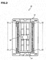
- the IC package 10 is inserted in the cover 16 through an IC package insertion opening 60 formed on the cover 16 and is accommodated in the socket main body 14.
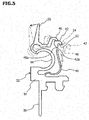
- the connection terminals 30 of the IC package 10 are brought into contact with the upper end surfaces of the first contacting portions 42, respectively, in one-to-one relationship. If the pressing down force acting on the cover 16 is then removed, the cover 16 returns to the original position due to the spring force of the coil spring 22. As a result, the second spring portion 44 displaces from the two-dot chain line position in FIG. 5 in the clockwise direction. As illustrated in FIG.
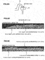
- the base material 62 is made of a conductive material. In the present embodiment, taking into consideration that elasticity is needed in the contact pin 32, for example, a beryllium copper (Be-Cu) alloy is employed. Furthermore, the underlying layer 64 is made of, for example, nickel (Ni) plating that is in the range of 2 ⁇ 10 -6 to 3 ⁇ 10 -6 m.
- the base material 62 and the underlying layer 64 are not limited to such materials, and they may be made of other suitably selected materials.
- the second layer 70 is formed on the first layer 68 by means of, for example, a manufacturing method using plating or a manufacturing method using ion plating in the same way as the above-described manufacturing method of the first layer 68.
- the first layer is a plating layer of Pd which is employed among materials into which Sn dissolves and diffuses by applying heat.
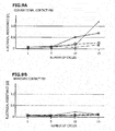
- Pd plating layer diffusion speed of Sn is extremely high and absorption amount of Sn is extremely large which are similar to Au.
- Mechanical strength of a Pd-Sn alloy is extremely higher than that of an Au-Sn alloy.
- the second layer is further formed on a contact side of the first layer, and the second layer is a plating layer of Ag. Ag is a material, into which Sn dissolves and diffuses by applying heat, in which diffusion speed of Sn is lower than that in the first layer. Accordingly, the speed at which Sn contained in the connection terminal 30 of the IC package 10 dissolves into the contact pin side becomes slow.
Landscapes
- Chemical & Material Sciences (AREA)
- Engineering & Computer Science (AREA)
- Materials Engineering (AREA)
- Metallurgy (AREA)
- Organic Chemistry (AREA)
- Mechanical Engineering (AREA)
- Chemical Kinetics & Catalysis (AREA)
- General Chemical & Material Sciences (AREA)
- Electrochemistry (AREA)
- Testing Of Individual Semiconductor Devices (AREA)
- Connecting Device With Holders (AREA)
- Automation & Control Theory (AREA)
- Manufacturing & Machinery (AREA)
Applications Claiming Priority (2)
| Application Number | Priority Date | Filing Date | Title |
|---|---|---|---|
| JP2013057696A JP2014182976A (ja) | 2013-03-21 | 2013-03-21 | 電気接触子及び電気部品用ソケット |
| PCT/JP2014/056788 WO2014148365A1 (fr) | 2013-03-21 | 2014-03-13 | Connecteur électrique et douille pour composant électrique |
Publications (3)
| Publication Number | Publication Date |
|---|---|
| EP2978076A1 true EP2978076A1 (fr) | 2016-01-27 |
| EP2978076A4 EP2978076A4 (fr) | 2016-11-02 |
| EP2978076B1 EP2978076B1 (fr) | 2019-01-02 |
Family
ID=51580051
Family Applications (1)
| Application Number | Title | Priority Date | Filing Date |
|---|---|---|---|
| EP14770603.0A Active EP2978076B1 (fr) | 2013-03-21 | 2014-03-13 | Connecteur électrique et douille pour composant électrique |
Country Status (7)
| Country | Link |
|---|---|
| US (1) | US20160285186A1 (fr) |
| EP (1) | EP2978076B1 (fr) |
| JP (1) | JP2014182976A (fr) |
| KR (1) | KR20150135336A (fr) |
| CN (1) | CN105051982B (fr) |
| TW (1) | TWI620380B (fr) |
| WO (1) | WO2014148365A1 (fr) |
Cited By (2)
| Publication number | Priority date | Publication date | Assignee | Title |
|---|---|---|---|---|
| EP3343704A4 (fr) * | 2015-08-25 | 2019-04-24 | Enplas Corporation | Contact électrique et douille pour composant électrique |
| CN109845041A (zh) * | 2016-10-20 | 2019-06-04 | 株式会社自动网络技术研究所 | 连接端子及连接端子的制造方法 |
Families Citing this family (4)
| Publication number | Priority date | Publication date | Assignee | Title |
|---|---|---|---|---|
| KR101558256B1 (ko) * | 2015-05-18 | 2015-10-12 | 주식회사 기가레인 | 고정 가능한 프로브 핀 및 프로브 핀 고정 어셈블리 |
| JP6755096B2 (ja) * | 2016-01-22 | 2020-09-16 | 日立オートモティブシステムズ株式会社 | 車載用電子モジュール、カードエッジコネクタ、およびコネクタ |
| KR101723975B1 (ko) * | 2016-12-15 | 2017-04-07 | 주식회사 제이미크론 | 휴대폰 방수용 충전단자 및 이의 제조방법 |
| JP6653340B2 (ja) * | 2018-02-01 | 2020-02-26 | Jx金属株式会社 | バーンインテストソケット用表面処理金属材料、それを用いたバーンインテストソケット用コネクタ及びバーンインテストソケット |
Family Cites Families (16)
| Publication number | Priority date | Publication date | Assignee | Title |
|---|---|---|---|---|
| US3951872A (en) * | 1973-12-03 | 1976-04-20 | P. R. Mallory & Co., Inc. | Electrical contact material |
| JPS59180908A (ja) * | 1983-03-30 | 1984-10-15 | 古河電気工業株式会社 | 銀被覆導体とその製造方法 |
| JPS6037605A (ja) * | 1983-08-11 | 1985-02-27 | 古河電気工業株式会社 | Ag被覆Cu系電子部品材料 |
| US4628165A (en) * | 1985-09-11 | 1986-12-09 | Learonal, Inc. | Electrical contacts and methods of making contacts by electrodeposition |
| US4911798A (en) * | 1988-12-20 | 1990-03-27 | At&T Bell Laboratories | Palladium alloy plating process |
| GB9102062D0 (en) * | 1991-01-31 | 1991-03-13 | Otter Controls Ltd | Improvements relating to conductors for switching applications |
| DE19543223C1 (de) * | 1995-11-20 | 1997-02-20 | Degussa | Silber-Eisen-Werkstoff für elektrische Schaltkontakte (III) |
| US6352634B1 (en) * | 1998-06-10 | 2002-03-05 | W. C. Heraeus Gmbh & Co. Kg | Method for producing a lead-free substrate |
| US20020185716A1 (en) * | 2001-05-11 | 2002-12-12 | Abys Joseph Anthony | Metal article coated with multilayer finish inhibiting whisker growth |
| US7391116B2 (en) * | 2003-10-14 | 2008-06-24 | Gbc Metals, Llc | Fretting and whisker resistant coating system and method |
| JP4728571B2 (ja) * | 2003-10-31 | 2011-07-20 | 古河電気工業株式会社 | 可動接点用銀被覆ステンレス条の製造方法 |
| JP5334416B2 (ja) | 2005-09-22 | 2013-11-06 | 株式会社エンプラス | 電気接触子及び電気部品用ソケット |
| JP4834023B2 (ja) * | 2007-03-27 | 2011-12-07 | 古河電気工業株式会社 | 可動接点部品用銀被覆材およびその製造方法 |
| CN106086502B (zh) * | 2010-03-12 | 2018-12-04 | 克斯塔里克公司 | 具有涂层的物件及涂布方法 |
| EP2860533B1 (fr) * | 2012-06-06 | 2020-12-02 | Enplas Corporation | Prise femelle pour composant électrique |
| WO2014003003A1 (fr) * | 2012-06-25 | 2014-01-03 | 山一電機株式会社 | Contact d'essai électrique et alvéole d'essai électrique l'utilisant |
-
2013
- 2013-03-21 JP JP2013057696A patent/JP2014182976A/ja active Pending
-
2014
- 2014-03-13 EP EP14770603.0A patent/EP2978076B1/fr active Active
- 2014-03-13 US US14/778,573 patent/US20160285186A1/en not_active Abandoned
- 2014-03-13 KR KR1020157027479A patent/KR20150135336A/ko not_active Ceased
- 2014-03-13 CN CN201480017235.XA patent/CN105051982B/zh active Active
- 2014-03-13 WO PCT/JP2014/056788 patent/WO2014148365A1/fr not_active Ceased
- 2014-03-21 TW TW103110644A patent/TWI620380B/zh active
Cited By (3)
| Publication number | Priority date | Publication date | Assignee | Title |
|---|---|---|---|---|
| EP3343704A4 (fr) * | 2015-08-25 | 2019-04-24 | Enplas Corporation | Contact électrique et douille pour composant électrique |
| CN109845041A (zh) * | 2016-10-20 | 2019-06-04 | 株式会社自动网络技术研究所 | 连接端子及连接端子的制造方法 |
| CN109845041B (zh) * | 2016-10-20 | 2020-10-23 | 株式会社自动网络技术研究所 | 连接端子及连接端子的制造方法 |
Also Published As
| Publication number | Publication date |
|---|---|
| TW201503492A (zh) | 2015-01-16 |
| WO2014148365A1 (fr) | 2014-09-25 |
| JP2014182976A (ja) | 2014-09-29 |
| KR20150135336A (ko) | 2015-12-02 |
| CN105051982B (zh) | 2018-09-14 |
| EP2978076B1 (fr) | 2019-01-02 |
| EP2978076A4 (fr) | 2016-11-02 |
| CN105051982A (zh) | 2015-11-11 |
| US20160285186A1 (en) | 2016-09-29 |
| TWI620380B (zh) | 2018-04-01 |
Similar Documents
| Publication | Publication Date | Title |
|---|---|---|
| EP2978076B1 (fr) | Connecteur électrique et douille pour composant électrique | |
| JP6112792B2 (ja) | 電気接触子の使用方法及び電気接触子 | |
| EP2860533A1 (fr) | Contacteur électrique et prise femelle pour composant électrique | |
| CN106847720B (zh) | 半导体装置的制造方法 | |
| JP6241502B2 (ja) | 電気テスト用コンタクトおよびそれを用いた電気テスト用ソケット | |
| US9698511B2 (en) | Electric contact and socket for electrical part | |
| TWI697155B (zh) | 電子連接器及電子零件插座 | |
| JP2012184987A (ja) | 半導体装置の検査方法 | |
| JP6506590B2 (ja) | 電気接触子及び電気部品用ソケット | |
| JP2005268090A (ja) | コンタクトピン及び電気部品用ソケット |
Legal Events
| Date | Code | Title | Description |
|---|---|---|---|
| PUAI | Public reference made under article 153(3) epc to a published international application that has entered the european phase |
Free format text: ORIGINAL CODE: 0009012 |
|
| 17P | Request for examination filed |
Effective date: 20151021 |
|
| AK | Designated contracting states |
Kind code of ref document: A1 Designated state(s): AL AT BE BG CH CY CZ DE DK EE ES FI FR GB GR HR HU IE IS IT LI LT LU LV MC MK MT NL NO PL PT RO RS SE SI SK SM TR |
|
| AX | Request for extension of the european patent |
Extension state: BA ME |
|
| DAX | Request for extension of the european patent (deleted) | ||
| A4 | Supplementary search report drawn up and despatched |
Effective date: 20160930 |
|
| RIC1 | Information provided on ipc code assigned before grant |
Ipc: H01R 12/70 20110101ALN20160926BHEP Ipc: C23C 14/32 20060101ALN20160926BHEP Ipc: C23C 18/16 20060101ALN20160926BHEP Ipc: H01R 13/03 20060101AFI20160926BHEP Ipc: C25D 5/12 20060101ALN20160926BHEP Ipc: C25D 5/10 20060101ALN20160926BHEP |
|
| STAA | Information on the status of an ep patent application or granted ep patent |
Free format text: STATUS: EXAMINATION IS IN PROGRESS |
|
| 17Q | First examination report despatched |
Effective date: 20171030 |
|
| GRAP | Despatch of communication of intention to grant a patent |
Free format text: ORIGINAL CODE: EPIDOSNIGR1 |
|
| STAA | Information on the status of an ep patent application or granted ep patent |
Free format text: STATUS: GRANT OF PATENT IS INTENDED |
|
| RIC1 | Information provided on ipc code assigned before grant |
Ipc: C25D 5/12 20060101ALI20180615BHEP Ipc: C25D 5/10 20060101ALI20180615BHEP Ipc: H01R 13/03 20060101AFI20180615BHEP Ipc: C22C 5/06 20060101ALI20180615BHEP Ipc: C23C 18/16 20060101ALI20180615BHEP Ipc: B32B 15/01 20060101ALI20180615BHEP Ipc: C22C 5/04 20060101ALI20180615BHEP Ipc: C25D 7/00 20060101ALI20180615BHEP |
|
| INTG | Intention to grant announced |
Effective date: 20180720 |
|
| GRAS | Grant fee paid |
Free format text: ORIGINAL CODE: EPIDOSNIGR3 |
|
| GRAA | (expected) grant |
Free format text: ORIGINAL CODE: 0009210 |
|
| STAA | Information on the status of an ep patent application or granted ep patent |
Free format text: STATUS: THE PATENT HAS BEEN GRANTED |
|
| AK | Designated contracting states |
Kind code of ref document: B1 Designated state(s): AL AT BE BG CH CY CZ DE DK EE ES FI FR GB GR HR HU IE IS IT LI LT LU LV MC MK MT NL NO PL PT RO RS SE SI SK SM TR |
|
| REG | Reference to a national code |
Ref country code: GB Ref legal event code: FG4D |
|
| REG | Reference to a national code |
Ref country code: CH Ref legal event code: EP Ref country code: AT Ref legal event code: REF Ref document number: 1085596 Country of ref document: AT Kind code of ref document: T Effective date: 20190115 |
|
| REG | Reference to a national code |
Ref country code: IE Ref legal event code: FG4D |
|
| REG | Reference to a national code |
Ref country code: DE Ref legal event code: R096 Ref document number: 602014039175 Country of ref document: DE |
|
| REG | Reference to a national code |
Ref country code: NL Ref legal event code: MP Effective date: 20190102 |
|
| REG | Reference to a national code |
Ref country code: LT Ref legal event code: MG4D |
|
| REG | Reference to a national code |
Ref country code: AT Ref legal event code: MK05 Ref document number: 1085596 Country of ref document: AT Kind code of ref document: T Effective date: 20190102 |
|
| PG25 | Lapsed in a contracting state [announced via postgrant information from national office to epo] |
Ref country code: NL Free format text: LAPSE BECAUSE OF FAILURE TO SUBMIT A TRANSLATION OF THE DESCRIPTION OR TO PAY THE FEE WITHIN THE PRESCRIBED TIME-LIMIT Effective date: 20190102 |
|
| PG25 | Lapsed in a contracting state [announced via postgrant information from national office to epo] |
Ref country code: LT Free format text: LAPSE BECAUSE OF FAILURE TO SUBMIT A TRANSLATION OF THE DESCRIPTION OR TO PAY THE FEE WITHIN THE PRESCRIBED TIME-LIMIT Effective date: 20190102 Ref country code: SE Free format text: LAPSE BECAUSE OF FAILURE TO SUBMIT A TRANSLATION OF THE DESCRIPTION OR TO PAY THE FEE WITHIN THE PRESCRIBED TIME-LIMIT Effective date: 20190102 Ref country code: ES Free format text: LAPSE BECAUSE OF FAILURE TO SUBMIT A TRANSLATION OF THE DESCRIPTION OR TO PAY THE FEE WITHIN THE PRESCRIBED TIME-LIMIT Effective date: 20190102 Ref country code: PT Free format text: LAPSE BECAUSE OF FAILURE TO SUBMIT A TRANSLATION OF THE DESCRIPTION OR TO PAY THE FEE WITHIN THE PRESCRIBED TIME-LIMIT Effective date: 20190502 Ref country code: NO Free format text: LAPSE BECAUSE OF FAILURE TO SUBMIT A TRANSLATION OF THE DESCRIPTION OR TO PAY THE FEE WITHIN THE PRESCRIBED TIME-LIMIT Effective date: 20190402 Ref country code: PL Free format text: LAPSE BECAUSE OF FAILURE TO SUBMIT A TRANSLATION OF THE DESCRIPTION OR TO PAY THE FEE WITHIN THE PRESCRIBED TIME-LIMIT Effective date: 20190102 Ref country code: FI Free format text: LAPSE BECAUSE OF FAILURE TO SUBMIT A TRANSLATION OF THE DESCRIPTION OR TO PAY THE FEE WITHIN THE PRESCRIBED TIME-LIMIT Effective date: 20190102 |
|
| PG25 | Lapsed in a contracting state [announced via postgrant information from national office to epo] |
Ref country code: BG Free format text: LAPSE BECAUSE OF FAILURE TO SUBMIT A TRANSLATION OF THE DESCRIPTION OR TO PAY THE FEE WITHIN THE PRESCRIBED TIME-LIMIT Effective date: 20190402 Ref country code: RS Free format text: LAPSE BECAUSE OF FAILURE TO SUBMIT A TRANSLATION OF THE DESCRIPTION OR TO PAY THE FEE WITHIN THE PRESCRIBED TIME-LIMIT Effective date: 20190102 Ref country code: LV Free format text: LAPSE BECAUSE OF FAILURE TO SUBMIT A TRANSLATION OF THE DESCRIPTION OR TO PAY THE FEE WITHIN THE PRESCRIBED TIME-LIMIT Effective date: 20190102 Ref country code: IS Free format text: LAPSE BECAUSE OF FAILURE TO SUBMIT A TRANSLATION OF THE DESCRIPTION OR TO PAY THE FEE WITHIN THE PRESCRIBED TIME-LIMIT Effective date: 20190502 Ref country code: GR Free format text: LAPSE BECAUSE OF FAILURE TO SUBMIT A TRANSLATION OF THE DESCRIPTION OR TO PAY THE FEE WITHIN THE PRESCRIBED TIME-LIMIT Effective date: 20190403 Ref country code: HR Free format text: LAPSE BECAUSE OF FAILURE TO SUBMIT A TRANSLATION OF THE DESCRIPTION OR TO PAY THE FEE WITHIN THE PRESCRIBED TIME-LIMIT Effective date: 20190102 |
|
| REG | Reference to a national code |
Ref country code: DE Ref legal event code: R097 Ref document number: 602014039175 Country of ref document: DE |
|
| PG25 | Lapsed in a contracting state [announced via postgrant information from national office to epo] |
Ref country code: AL Free format text: LAPSE BECAUSE OF FAILURE TO SUBMIT A TRANSLATION OF THE DESCRIPTION OR TO PAY THE FEE WITHIN THE PRESCRIBED TIME-LIMIT Effective date: 20190102 Ref country code: MC Free format text: LAPSE BECAUSE OF FAILURE TO SUBMIT A TRANSLATION OF THE DESCRIPTION OR TO PAY THE FEE WITHIN THE PRESCRIBED TIME-LIMIT Effective date: 20190102 Ref country code: DK Free format text: LAPSE BECAUSE OF FAILURE TO SUBMIT A TRANSLATION OF THE DESCRIPTION OR TO PAY THE FEE WITHIN THE PRESCRIBED TIME-LIMIT Effective date: 20190102 Ref country code: SK Free format text: LAPSE BECAUSE OF FAILURE TO SUBMIT A TRANSLATION OF THE DESCRIPTION OR TO PAY THE FEE WITHIN THE PRESCRIBED TIME-LIMIT Effective date: 20190102 Ref country code: EE Free format text: LAPSE BECAUSE OF FAILURE TO SUBMIT A TRANSLATION OF THE DESCRIPTION OR TO PAY THE FEE WITHIN THE PRESCRIBED TIME-LIMIT Effective date: 20190102 Ref country code: IT Free format text: LAPSE BECAUSE OF FAILURE TO SUBMIT A TRANSLATION OF THE DESCRIPTION OR TO PAY THE FEE WITHIN THE PRESCRIBED TIME-LIMIT Effective date: 20190102 Ref country code: AT Free format text: LAPSE BECAUSE OF FAILURE TO SUBMIT A TRANSLATION OF THE DESCRIPTION OR TO PAY THE FEE WITHIN THE PRESCRIBED TIME-LIMIT Effective date: 20190102 Ref country code: RO Free format text: LAPSE BECAUSE OF FAILURE TO SUBMIT A TRANSLATION OF THE DESCRIPTION OR TO PAY THE FEE WITHIN THE PRESCRIBED TIME-LIMIT Effective date: 20190102 Ref country code: CZ Free format text: LAPSE BECAUSE OF FAILURE TO SUBMIT A TRANSLATION OF THE DESCRIPTION OR TO PAY THE FEE WITHIN THE PRESCRIBED TIME-LIMIT Effective date: 20190102 |
|
| REG | Reference to a national code |
Ref country code: CH Ref legal event code: PL |
|
| PLBE | No opposition filed within time limit |
Free format text: ORIGINAL CODE: 0009261 |
|
| STAA | Information on the status of an ep patent application or granted ep patent |
Free format text: STATUS: NO OPPOSITION FILED WITHIN TIME LIMIT |
|
| PG25 | Lapsed in a contracting state [announced via postgrant information from national office to epo] |
Ref country code: SM Free format text: LAPSE BECAUSE OF FAILURE TO SUBMIT A TRANSLATION OF THE DESCRIPTION OR TO PAY THE FEE WITHIN THE PRESCRIBED TIME-LIMIT Effective date: 20190102 Ref country code: LU Free format text: LAPSE BECAUSE OF NON-PAYMENT OF DUE FEES Effective date: 20190313 |
|
| REG | Reference to a national code |
Ref country code: BE Ref legal event code: MM Effective date: 20190331 |
|
| 26N | No opposition filed |
Effective date: 20191003 |
|
| GBPC | Gb: european patent ceased through non-payment of renewal fee |
Effective date: 20190402 |
|
| PG25 | Lapsed in a contracting state [announced via postgrant information from national office to epo] |
Ref country code: CH Free format text: LAPSE BECAUSE OF NON-PAYMENT OF DUE FEES Effective date: 20190331 Ref country code: GB Free format text: LAPSE BECAUSE OF NON-PAYMENT OF DUE FEES Effective date: 20190402 Ref country code: LI Free format text: LAPSE BECAUSE OF NON-PAYMENT OF DUE FEES Effective date: 20190331 Ref country code: IE Free format text: LAPSE BECAUSE OF NON-PAYMENT OF DUE FEES Effective date: 20190313 |
|
| PG25 | Lapsed in a contracting state [announced via postgrant information from national office to epo] |
Ref country code: SI Free format text: LAPSE BECAUSE OF FAILURE TO SUBMIT A TRANSLATION OF THE DESCRIPTION OR TO PAY THE FEE WITHIN THE PRESCRIBED TIME-LIMIT Effective date: 20190102 Ref country code: BE Free format text: LAPSE BECAUSE OF NON-PAYMENT OF DUE FEES Effective date: 20190331 |
|
| PG25 | Lapsed in a contracting state [announced via postgrant information from national office to epo] |
Ref country code: TR Free format text: LAPSE BECAUSE OF FAILURE TO SUBMIT A TRANSLATION OF THE DESCRIPTION OR TO PAY THE FEE WITHIN THE PRESCRIBED TIME-LIMIT Effective date: 20190102 |
|
| PG25 | Lapsed in a contracting state [announced via postgrant information from national office to epo] |
Ref country code: CY Free format text: LAPSE BECAUSE OF FAILURE TO SUBMIT A TRANSLATION OF THE DESCRIPTION OR TO PAY THE FEE WITHIN THE PRESCRIBED TIME-LIMIT Effective date: 20190102 |
|
| PG25 | Lapsed in a contracting state [announced via postgrant information from national office to epo] |
Ref country code: HU Free format text: LAPSE BECAUSE OF FAILURE TO SUBMIT A TRANSLATION OF THE DESCRIPTION OR TO PAY THE FEE WITHIN THE PRESCRIBED TIME-LIMIT; INVALID AB INITIO Effective date: 20140313 |
|
| PG25 | Lapsed in a contracting state [announced via postgrant information from national office to epo] |
Ref country code: MK Free format text: LAPSE BECAUSE OF FAILURE TO SUBMIT A TRANSLATION OF THE DESCRIPTION OR TO PAY THE FEE WITHIN THE PRESCRIBED TIME-LIMIT Effective date: 20190102 |
|
| P01 | Opt-out of the competence of the unified patent court (upc) registered |
Effective date: 20230512 |
|
| PGFP | Annual fee paid to national office [announced via postgrant information from national office to epo] |
Ref country code: DE Payment date: 20260319 Year of fee payment: 13 |
|
| PGFP | Annual fee paid to national office [announced via postgrant information from national office to epo] |
Ref country code: FR Payment date: 20260320 Year of fee payment: 13 |
|
| PGFP | Annual fee paid to national office [announced via postgrant information from national office to epo] |
Ref country code: MT Payment date: 20260226 Year of fee payment: 13 |