EP2980278A1 - Composant électroformé et son procédé de fabrication - Google Patents
Composant électroformé et son procédé de fabrication Download PDFInfo
- Publication number
- EP2980278A1 EP2980278A1 EP14831220.0A EP14831220A EP2980278A1 EP 2980278 A1 EP2980278 A1 EP 2980278A1 EP 14831220 A EP14831220 A EP 14831220A EP 2980278 A1 EP2980278 A1 EP 2980278A1
- Authority
- EP
- European Patent Office
- Prior art keywords
- insulating film
- electroformed
- insulating
- electroformed product
- mold form
- Prior art date
- Legal status (The legal status is an assumption and is not a legal conclusion. Google has not performed a legal analysis and makes no representation as to the accuracy of the status listed.)
- Granted
Links
Images






Classifications
-
- C—CHEMISTRY; METALLURGY
- C25—ELECTROLYTIC OR ELECTROPHORETIC PROCESSES; APPARATUS THEREFOR
- C25D—PROCESSES FOR THE ELECTROLYTIC OR ELECTROPHORETIC PRODUCTION OF COATINGS; ELECTROFORMING; APPARATUS THEREFOR
- C25D1/00—Electroforming
- C25D1/003—3D structures, e.g. superposed patterned layers
-
- C—CHEMISTRY; METALLURGY
- C25—ELECTROLYTIC OR ELECTROPHORETIC PROCESSES; APPARATUS THEREFOR
- C25D—PROCESSES FOR THE ELECTROLYTIC OR ELECTROPHORETIC PRODUCTION OF COATINGS; ELECTROFORMING; APPARATUS THEREFOR
- C25D1/00—Electroforming
-
- C—CHEMISTRY; METALLURGY
- C25—ELECTROLYTIC OR ELECTROPHORETIC PROCESSES; APPARATUS THEREFOR
- C25D—PROCESSES FOR THE ELECTROLYTIC OR ELECTROPHORETIC PRODUCTION OF COATINGS; ELECTROFORMING; APPARATUS THEREFOR
- C25D1/00—Electroforming
- C25D1/10—Moulds; Masks; Masterforms
-
- C—CHEMISTRY; METALLURGY
- C25—ELECTROLYTIC OR ELECTROPHORETIC PROCESSES; APPARATUS THEREFOR
- C25D—PROCESSES FOR THE ELECTROLYTIC OR ELECTROPHORETIC PRODUCTION OF COATINGS; ELECTROFORMING; APPARATUS THEREFOR
- C25D1/00—Electroforming
- C25D1/20—Separation of the formed objects from the electrodes with no destruction of said electrodes
-
- G—PHYSICS
- G01—MEASURING; TESTING
- G01R—MEASURING ELECTRIC VARIABLES; MEASURING MAGNETIC VARIABLES
- G01R1/00—Details of instruments or arrangements of the types included in groups G01R5/00 - G01R13/00 and G01R31/00
- G01R1/02—General constructional details
- G01R1/06—Measuring leads; Measuring probes
- G01R1/067—Measuring probes
- G01R1/06711—Probe needles; Cantilever beams; "Bump" contacts; Replaceable probe pins
- G01R1/06716—Elastic
- G01R1/06722—Spring-loaded
-
- G—PHYSICS
- G01—MEASURING; TESTING
- G01R—MEASURING ELECTRIC VARIABLES; MEASURING MAGNETIC VARIABLES
- G01R3/00—Apparatus or processes specially adapted for the manufacture or maintenance of measuring instruments, e.g. of probe tips
Definitions
- the present invention relates to an electroformed component and a method of producing the electroformed component.
- Fig. 1 is a perspective view illustrating a method of producing a conventional electroformed component, that is, a contact.
- a surface of an electrically conductive base material 11 is subjected to electrolytic degreasing as illustrated in (A) of Fig. 1 .
- a photoresist 12 is applied to the surface of the electrically conductive base material 11.
- a laser beam 13 is scanned, with the use of a direct writing exposure device, along a region of the surface of the photoresist 12, except for a region having a contact shape.
- the contacts are sometimes used in such a manner as to be arranged at narrow pitches while maintaining electrical insulation from each other.
- the contacts may be used for a probe card that carries out electrical inspection of a highly dense microcircuit board.
- an insulator is sandwiched between a pair of substrates, and contacts such as those described above are contained in respective through-holes made through the insulator.
- Each of the substrates has supporting holes so as to face the corresponding through-holes of the insulator. Both ends of each of the contacts are inserted into respective supporting holes of corresponding substrates.
- an end part of each of the contacts comes into contact with a corresponding electrode (inter-electrode pitch: 30 ⁇ m to 200 ⁇ m) of the microcircuit board to be measured. Therefore, narrow pitches between the electrodes of the microcircuit board to be measured make it necessary to provide the contacts to be arranged at narrow pitches as well.
- An electroformed component production method of the present invention includes: an electrodepositing step of fabricating an electroformed product by electrodepositing a metal on an exposed surface which is at least part of an electrically conductive base material and which is exposed within an opening of an insulating mold form; a mold form removing step of removing the insulating mold form from a surface of the electrically conductive base material; an insulating film forming step of covering a surface of the electroformed product with an insulating film; and an insulating film removing step of removing part of the insulating film while causing a remaining part of the insulating film to remain on at least part of the surface of the electroformed product.
- FIG. 1 are perspective views for describing a step of producing conventional contacts.
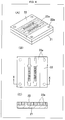
- FIG. 2 are a perspective view, a plan view and a cross-sectional view, respectively, which illustrate a step of electrolytic degreasing an electrically conductive base material in accordance with Embodiment 1 of the present invention.
- FIG. 3 are a perspective view, a plan view and a cross-sectional view, respectively, which illustrate a step of laminating a dry film resist in accordance with Embodiment 1 of the present invention.
- FIG. 4 are a perspective view and a plan view, respectively, which illustrate a step of exposing the dry film resist in accordance with Embodiment 1 of the present invention.
- (C) of Fig. 4 is a cross-sectional view taken along the line X-X shown in (B) of Fig. 4 .
- FIG. 5 are a perspective view, a plan view and a cross-sectional view, respectively, which illustrate a step of fabricating a mold form by developing the dry film resist in accordance with Embodiment 1 of the present invention.
- FIG. 6 are a perspective view, a plan view and a cross-sectional view, respectively, which illustrate a step of electroforming in accordance with Embodiment 1 of the present invention.
- FIG. 7 are a perspective view, a plan view and a cross-sectional view, respectively, which illustrate a step of removing the mold form in accordance with Embodiment 1 of the present invention.
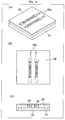
- FIG. 8 are a perspective view, a plan view and a cross-sectional view, respectively, which illustrate a step of laminating an insulating film (dry film resist) in accordance with Embodiment 1 of the present invention.
- FIG. 9 are a perspective view, a plan view and a cross-sectional view, respectively, which illustrate an step of exposing the insulating film in accordance with Embodiment 1 of the present invention.
- FIG. 10 are a perspective view, a plan view and a cross-sectional view, respectively, which illustrate a developing the insulating film in accordance with Embodiment 1 of the present invention.
- FIG. 11 are a perspective view, a plan view and a cross-sectional view, respectively, which illustrate a step of peeling electroformed components in accordance with Embodiment 1 of the present invention.
- FIG. 12 are a perspective view and a plan view, respectively, which illustrate a step of making position determining holes through an electrically conductive base material in accordance with Embodiment 2 of the present invention.
- (C) of Fig. 12 is a cross-sectional view taken along the line Y-Y shown in (B) of Fig. 12 .
- FIG. 13 are a perspective view, a plan view and a cross-sectional view, respectively, which illustrate a step of laminating a dry film resist in accordance with Embodiment 2 of the present invention.
- FIG. 14 are a perspective view, a plan view and a cross-sectional view, respectively, which illustrate a step of exposing the dry film resist in accordance with Embodiment 2 of the present invention.
- FIG. 15 are a perspective view, a plan view and a cross-sectional view, respectively, which illustrate a step of fabricating a mold form by developing the dry film resist in accordance with Embodiment 2 of the present invention.
- FIG. 16 are a perspective view, a plan view and a cross-sectional view, respectively, which illustrate a step of electroforming in accordance with Embodiment 2 of the present invention.
- FIG. 17 are a perspective view, a plan view and a cross-sectional view, respectively, which illustrate a step of removing a mold form in accordance with Embodiment 2 of the present invention.
- FIG. 18 are a perspective view, a plan view and a cross-sectional view, respectively, which illustrate a step of laminating an insulating film (dry film resist) in accordance with Embodiment 2 of the present invention.
- FIG. 19 are a perspective view, a plan view and a cross-sectional view, respectively, which illustrate a step of exposing the insulating film in accordance with Embodiment 2 of the present invention.
- FIG. 20 are a perspective view, a plan view and a cross-sectional view, respectively, which illustrate a step of developing the insulating film in accordance with Embodiment 2 of the present invention.
- FIG. 21 are a perspective view, a plan view and a cross-sectional view, respectively, which illustrate a step of peeling electroformed components in accordance with Embodiment 2 of the present invention.
- FIG. 22 are a front view and a perspective view, respectively, each of which illustrates a contact obtained by providing an insulating film all over a surface of a contact element (electroformed product).
- FIG. 23 are a front view and a perspective view, respectively, each of which illustrates a contact obtained by providing an insulating film on part of a contact element (electroformed product).
- FIG. 24 are a front view and a perspective view, respectively, each of which illustrates another contact obtained by providing an insulating film on part of a contact element (electroformed product).
- Fig. 25 is a front view illustrating yet another contact obtained by providing an insulating film on part of a contact element (electroformed product).
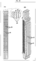
- FIG. 26 are a side view and a perspective view, respectively, each of which illustrates contacts configured so that respective contact elements (electroformed products), on each of which an insulating film is provided, are arranged at narrow pitches.
- an electrically conductive base material 21 is first subjected to electrolytic degreasing.
- (A) of Fig. 2 , (B) of Fig. 2 and (C) of Fig. 2 are a perspective view, a plan view and a cross-sectional view, respectively, which illustrate a step involved in the electrolytic degreasing ((A), (B) and (C) of each of Figs. 3 to 11 are also a perspective view, a plan view and a cross-sectional view, respectively).
- the electrically conductive base material 21 is a stainless plate having flat surfaces.
- At least a top surface of the electrically conductive base material 21 has been processed so that a metal molded product, which has been electrodeposited on the top surface, can easily be peeled off.
- the electrically conductive base material 21 is degreased and cleaned in a step of electrolytic degreasing (electrolytic cleaning).
- the electrolytic degreasing is a process of degreasing the electrically conductive base material 21 by (i) causing the electrically conductive base material 21 to serve as a cathode or an anode in an alkaline solution or (ii) causing a polarity of the electrically conductive base material 21 to alternate.
- a negative dry film resist 22 comes into close contact with the top surface of the electrically conductive base material 21 so as to be laminated on the top surface of the electrically conductive base material 21.
- the dry film resist 22 is greater in thickness than an electroformed product (contact element 25).
- the thickness of the dry film resist 22 is preferably several tens of micrometers or more. While the dry film resist 22 is preferable for facilitating the step, it is alternatively possible to use a liquid resist. For example, it is possible to apply a liquid resist to the top surface of the electrically conductive base material 21 and then carry out prebaking.
- the dry film resist 22 is irradiated with an ultraviolet laser beam with the use of a direct writing exposure device, so that an area inside a predetermined region is scanned.
- (A) of Fig. 4 , (B) of Fig. 4 and (C) of Fig. 4 illustrate the exposed region.
- an ultraviolet laser beam is scanned along regions 22a (which are obtained by providing a dot pattern on the dry film resist 22) for light exposure (see (A) of Fig. 4 )).
- the ultraviolet laser beam is scanned along regions other than regions from which contact elements (25) and frame parts (26) are to be fabricated.
- regions, at which position determining marks are to be provided on the frame parts are also irradiated with the ultraviolet laser beam. According to the direct writing exposure method, it is thus unnecessary to use a mask. This allows an exposing step to be simple, and therefore allows for a reduction in cost. Nevertheless, the present invention does not exclude light exposure with the use of a mask.
- the dry film resist 22 which has been exposed to the light, is developed and rinsed. This causes the regions of the negative dry film resist 22, other than the exposed regions 22a, to be removed by a developing solution. A remaining part of the dry film resist 22 becomes a mold form 22b.
- This as illustrated in (A) of Fig. 5 , (B) of Fig. 5 and (C) of Fig. 5 , (i) causes cavities 23 for forming electroformed products to be fabricated in the mold form 22b and (ii) causes the electrically conductive base material 21 to be exposed at bottom surfaces of the cavities 23.
- parts of the dry film resist 22, which parts correspond to frame regions at which the frame parts are to be formed are peeled and (ii) protrusion parts 24, which are intended for forming the position determining marks in the frame regions, are formed.
- the contact elements 25 are formed by electroforming (electroforming method) with the use of the electrically conductive base material 21 and the mold form 22b which serve as a matrix.
- an electrodepositing step is carried out such that (i) the matrix is provided in an electrolytic cell and then (ii) an electric current flows through an electrolytic solution by applying, with the use of a direct power supply, a voltage between the electrically conductive base material 21 and a counter electrode.
- metal ions in the electrolytic solution are electrodeposited on the surfaces of the electrically conductive base material 21. This causes metal to be precipitated. Meanwhile, the mold form blocks the electric current.
- a metal grows, in each of the cavities 23, in a voltage application direction d from the bottom surface, so that a contact element 25 is formed in each of the cavities 23.
- the contact element 25 thus grown includes (i) a spring part 44 which is elastically deformable in a direction f which is perpendicular to a voltage application direction and (ii) a terminal part 45 which is located so as to be able to be pressed, by elasticity of the spring part 44, against an external conductor (e.g. a terminal of an integrated circuit).
- frame parts 26 are formed outside the mold form 22b.
- a thickness of each of the metals (contact elements 25) thus electrodeposited is determined by an accumulated electric current flowing amount of the electric current (i.e. a time-based accumulated amount of the flowing electric current).
- an accumulated electric current flowing amount of the electric current i.e. a time-based accumulated amount of the flowing electric current.
- the mold form 22b is peeled by etching or the like.
- the mold form 22b has been peeled, as illustrated in (A) of Fig. 7 , (B) of Fig. 7 and (C) of Fig. 7 , the contact elements 25 remain attached to the top surface of the electrically conductive base material 21.
- position determining marks 27 are formed after the protrusion parts 24 are peeled, which position determining marks 27 each have a form of a through-hole.
- the position determining marks can be post-like protrusion parts which are formed by electroforming on the surface of the electrically conductive base material.
- the electrically conductive base material 21 is then covered, from above, with an insulating film 28 which is photosensitive (see (A) of Fig. 8 , (B) of Fig. 8 and (C) of Fig. 8 ). Then, the insulating film 28 comes into close contact with the top surfaces (main surfaces) of the contact elements 25 and of the frame parts 26.
- the insulating film 28 is a negative dry film resist.
- the insulating film 28 is irradiated with an ultraviolet laser beam with the use of a direct writing exposure device, so that an area inside a predetermined region is scanned.
- (A) of Fig. 9 , (B) of Fig. 9 and (C) of Fig. 9 illustrate the exposed region.
- an ultraviolet laser beam is, for example, scanned along regions 28a (which are obtained by providing a dot pattern on the insulating film 28) for light exposure (see (A) of Fig. 9 ). That is, in the case where the negative insulating film 28 is used, the ultraviolet laser beam is scanned along predetermined regions located directly above the respective contact elements 25.
- the direct writing exposure device (i) carries out image recognition of positions the respective position determining marks 27 which are visible through the insulating film 28 and then (ii) scans an ultraviolet laser beam with the position determining marks 27 serving as positional references.
- This allows an ultraviolet laser beam to be precisely scanned, for light exposure, along the predetermined regions located directly above the respective contact elements 25.
- the insulating film 28, which has been exposed to the light is developed and rinsed. This causes regions of the negative insulating film 28, other than the exposed regions 28a, to be removed by a developing solution.
- This causes insulating films 28 to be provided (i) all over the main surfaces (i.e. surfaces perpendicular to the voltage application direction during the electroforming) of the respective contact elements 25 or (ii) only on predetermined partial regions of the main surfaces.
- the contact elements 25 i.e. contacts 29 (electroformed components)
- the contact elements 25 which have the respective top surfaces on which the corresponding insulating films 28 are provided, are peeled from the electrically conductive base material 21 (see (A) of Fig. 11 , (B) of Fig. 11 and (C) of Fig. 11 ).
- Embodiment 2 an electroformed component production method in accordance with Embodiment 2 of the present invention.
- the electroformed component production method of Embodiment 2 is different from that of Embodiment 1 in terms of how a position of an exposed region is determined in an exposing step. Therefore, part of Embodiment 2, which part is similar to Embodiment 1, will be briefly described.
- a plurality of position determining marks are first made at respective predetermined positions of an electrically conductive base material 21 (see (A) of Fig. 12 , (B) of Fig. 12 and (C) of Fig. 12 ).
- (A) of Fig. 12 , (B) of Fig. 12 and (C) of Fig. 12 are a perspective view, a plan view and a cross-sectional view, respectively, which illustrate a step of making the position determining holes 31 ((A), (B) and (C) of each of Figs. 13 to 21 are also a perspective view, plan view and a cross-sectional view).
- the position determining holes 31 can be made by laser perforating or by drilling. Then, a surface of the electrically conductive base material 21, through which the position determining holes 31 are made, is cleaned and then subjected to electrolytic degreasing.
- position determining marks are the position determining holes 31 made through the electrically conductive base material 21.
- the position determining marks can be circular engraved marks, cross engraved marks or the like, or can be recess parts or the like.
- a negative dry film resist 22 comes into close contact with a top surface of the electrically conductive base material 21 so as to be laminated on the top surface of the electrically conductive base material 21.
- the dry film resist 22 is irradiated with an ultraviolet laser beam with the use of a direct writing exposure device, so that an area inside a predetermined region is scanned.
- (A) of Fig. 14, Fig. 14 and (C) of Fig. 14 illustrate the exposed region.
- an ultraviolet laser beam is scanned along regions 22a (which are obtained by providing a dot pattern on the dry film resist 22) for light exposure (see (A) of Fig. 4 )). That is, in the case where the negative dry film resist 22 is used, the ultraviolet laser beam is scanned along regions other than regions from which contact elements (25) and frame parts (26) are to be fabricated.
- the direct writing exposure device (i) carries out image recognition of positions the respective position determining holes 31 which are visible through the dry film resist 22 and then (ii) scans an ultraviolet laser beam with the position determining holes 31 serving as positional references.
- metals are precipitated, by electroforming (electroforming method), in a matrix made up of the electrically conductive base material 21 and the mold form 22b. This causes contact elements 25 to be formed in the respective cavities 23.
- the mold form 22b is peeled by etching or the like. This, as illustrated in (A) of Fig. 17 , (B) of Fig. 17 and (C) of Fig. 17 , causes the contact elements 25 to be provided on the top surface of the electrically conductive base material 21.
- the electrically conductive base material 21 is then covered, from above, with an insulating film 28 (dry film resist) which is photosensitive (see (A) of Fig. 18 , (B) of Fig. 18 and (C) of Fig. 18 ). Then, the insulating film 28 comes into close contact with the top surfaces of the contact elements 25. Then, the insulating film 28 is irradiated with an ultraviolet laser beam with the use of a direct writing exposure device, so that an area inside a predetermined region is scanned. (A) of Fig. 19, Fig. 19 and (C) of Fig. 19 illustrate the exposed region.
- an ultraviolet laser beam is, for example, scanned along regions 28a (which are obtained by providing a dot pattern on the insulating film 28) for light exposure (see (A) of Fig. 9 ). That is, in the case where the negative insulating film 28 is used, the ultraviolet laser beam is scanned along predetermined regions located directly above the respective contact elements 25. In so doing, the direct writing exposure device (i) carries out image recognition of positions the respective position determining holes 31 which are visible through the insulating film 28 and then (ii) scans an ultraviolet laser beam with the position determining holes 31 serving as positional references.
- the position determining holes 31 are thus used as the same references for controlling the exposed region both when the dry film resist 22 is subjected to direct writing light exposure and when the insulating film 28 is subjected to direct writing light exposure.
- This allows an ultraviolet laser beam to be precisely scanned, for light exposure, along the predetermined regions located directly above the respective contact elements 25. Therefore, it is possible to reduce an amount by which the respective positions of the contact elements 25 and of the insulating film 28 are shifted from each other.
- the insulating film 28, which has been exposed to the light is developed and rinsed.
- This causes regions of the negative insulating film 28, other than the exposed regions 28a, to be removed by a developing solution.
- the contact elements 25 i.e. contacts 29
- the contact elements 25 which have the respective top surfaces on which the corresponding insulating films 28 are provided, are peeled from the electrically conductive base material 21 (see (A) of Fig. 11 , (B) of Fig. 11 and (C) of Fig. 11 ).
- FIG. 22 and (B) of Fig. 22 are a front view and a perspective view, respectively, each of which illustrates each of contacts 41 (electroformed component) produced by a method such as that described above. That is, (A) of Fig. 22 and (B) of Fig. 22 each illustrate a contact element 25 on which an insulating film 28 is provided. The contact element 25 is to be used as an integrated circuit inspection probe.
- a spring part 44 is provided, in a zigzag pattern, between a fixed part 42 and a movable part 43. At an end part of the fixed part 42, a terminal part 45 is provided. The spring part 44, which connects the fixed part 42 and the movable part 43, is thin.
- the resistance between the fixed part 42 and the movable part 43 is made small by causing a movable contact segment 46a, which is provided on the movable part 43, and a movable contact segment 46b, which is provided on the fixed part 42, to be slidably in contact with each other.
- the insulating film 28 is provided all over a main surface on one side of the contact element 25 (i.e. surface perpendicular to a voltage application direction during electroforming).
- the contacts 41 are to be used, as described later, while being arranged at narrow pitches while maintaining electrical insulation of the contact elements 25 from each other.
- the contacts 41 are contained in a casing (not illustrated).
- the fixed parts 42 are fixed to the casing.
- the terminal parts 45 protrude from the casing. In such a state, the terminal parts 45 come in contact with corresponding terminals of an integrated circuit, and the movable parts 43 are pressed down. This causes the terminal parts 45 to be pressed, by elasticity of the spring parts 44, against the corresponding terminals of the integrated circuit. Then, for example, electrical conduction failure or the like of each of the terminals of the integrated circuit is inspected.
- FIG. 23 and (B) of Fig. 23 show another example of each of contacts produced by a method such as that described above.
- a contact 51 an insulating film 28 is provided all over, except for a region corresponding to a spring part 44, a main surface on one side of a contact element 25.
- the spring part 44 has an elastically deformable portion. Therefore, there is a risk that if the insulating film 28 is provided on the elastically deformable portion of the spring part 44, then the insulating film 28 may be peeled from the contact element 25 or may have a crack developed therein. Therefore, it is possible not to provide the insulating film 28 on the elastically deformable portion of the spring part 44.
- FIG. 24 and (B) of Fig. 24 show a modification of the contact 51 illustrated in Fig. 23 .
- an insulating film 28 is provided on an entire portion of a spring part 44 except for portions where deforming amounts are so large that stress can easily concentrated on the portions.
- the insulating film 28 is provided on straight portions of the spring part 44, which straight portions each have a relatively small deforming amount.
- FIG. 25 and (B) of Fig. 25 illustrate another example of each of contacts produced by a method such as that described above.
- a contact 53 an insulating film 28 is provided all over, except for a region corresponding to a terminal part 45, a main surface on one side of a contact element 25.
- the insulating film 28 is provided all over the main surface except for the region corresponding to the terminal part 45, and then the terminal part 45 is plated with Au, solder, or the like.
- each of Figs. 22 to 25 are to be used so as to be stacked with each other while sandwiching an insulating film 28 between adjacent contact elements 25 (see (A) of Fig. 26 and (B) of Fig. 26 ).
- This process of stacking the contacts together can be made easy by being carried out during the step of producing the contacts. Therefore, it is possible to precisely arrange, at narrow pitches, thin and extremely small contact elements while maintaining electrical insulation of the contact elements from each other.
- an insulating film was provided only on a main surface on one side of a contact element.
- an insulating film can be provided on both main surfaces of a contact element (not illustrated).
- an electroformed component production method of the present invention includes: an electrodepositing step of fabricating an electroformed product by electrodepositing a metal on an exposed surface which is at least part of an electrically conductive base material and which is exposed within an opening of an insulating mold form; a mold form removing step of removing the insulating mold form from a surface of the electrically conductive base material; an insulating film forming step of covering a surface of the electroformed product with an insulating film; and an insulating film removing step of removing part of the insulating film while causing a remaining part of the insulating film to remain on at least part of the surface of the electroformed product.
- the electroformed component production method of the present invention it is possible to provide an insulating film on a surface of an electroformed product during a step of producing the electroformed product. This allows a thin insulating film to be provided on at least part of the surface of the electroformed product. Therefore, in a case where (i) the electroformed product includes a plurality of electroformed products, (ii) the insulating film includes a plurality of insulating films, and (iii) the plurality of electroformed products and the plurality of insulating films are alternately stacked, it is possible to arrange the plurality of electroformed products at narrow pitches while maintaining electrical insulation of the electroformed products from each other.
- the insulating film is thus provided on the surface of the electroformed product during the step of producing the electroformed product. Therefore, in a case where the electroformed product includes a plurality of electroformed products, the plurality of electroformed products can be stacked together during a step of producing the electroformed products. This allows the electroformed products to be precisely stacked together with an excellent production yield.
- the insulating film covering the surface of the electroformed product can be a dry film resist or a liquid resist which has been applied to the surface of the electroformed product.
- the insulating film is a dry film resist, it is possible to facilitate the film forming step.
- the insulating mold form In order to fabricate the insulating mold form, it is only necessary to cause the part of the electrically conductive base material to be exposed in the opening by making the opening through part of an insulating mold form material which is provided on the surface of the electrically conductive base material (mold form fabricating step). After the insulating film removing step, it is only necessary to peel, from the electrically conductive base material, the electroformed product having the surface on which the remaining part of the insulating film is provided.
- the insulating film is a photosensitive film; and the insulating film removing step includes (i) an exposing step of irradiating, after the insulating film forming step, the insulating film with light while the electroformed product serves as a positional reference, so that a partial region, which corresponds to the at least part of the surface of the electroformed product, is made insoluble in a developing solution and (ii) a developing step of subjecting the insulating film to a development process, so as to remove a region of the insulating film, the region not having been made insoluble in the developing solution.
- it is possible to precisely pattern an insulating film by use of, for example, a negative resist and a photolithography technique.
- the insulating film is a photosensitive film; and the insulating film removing step includes (i) an exposing step of irradiating, after the insulating film forming step, the insulating film with light while the electroformed product serves as a positional reference, so that a region of the insulating film, which region is other than a partial region corresponding to the at least part of the surface of the electroformed product, is made soluble and (ii) a developing step of subjecting the insulating film to a development process, so as to remove the region of the insulating film.
- it is possible to precisely pattern an insulating film by use of, for example, a positive resist and a photolithography technique.
- the electroformed component production method further includes: a mold form fabricating step of (i) fabricating the insulating mold form by making the opening through an insulating mold form material which is provided on the surface of the electrically conductive base material and (ii) forming, with use of the insulating mold form material, a recess part or a protrusion part any of which is intended for fabricating a position determining mark, in the electrodepositing step, (i) the electroformed product being fabricated in the opening and (ii) the recess part or the protrusion part fabricating the position determining mark having a protruding form or a recessed form, respectively, and in the exposing step, light irradiation being carried out while the position determining mark serves as a positional reference.
- a mold form fabricating step of (i) fabricating the insulating mold form by making the opening through an insulating mold form material which is provided on the surface of the electrically conductive base material and (ii) forming, with use of the insulating mold
- the electroformed component production method further includes: a mold form material providing step of providing an insulating mold form material on a surface of the electrically conductive base material, which surface has a position determining mark; and a mold form fabricating step of fabricating the insulating mold form by making the opening through part of the insulating mold form material while the position determining mark serves as a positional reference, in the exposing step, light irradiation being carried out while the position determining mark serves as a positional reference.
- the electroformed component production method of the present invention can be used for, for example, a method of producing a contact which is an electroformed product.
- a contact of the present invention includes: an electroformed product including (i) a spring part which is elastically deformable in a direction perpendicular to a voltage application direction in which a voltage is applied during formation of the contact by electroforming and (ii) a terminal part provided so as to be able to be pressed, by the spring part, against an external conductor; and an insulating film provided on at least part of a main surface of the electroformed product, which main surface is perpendicular to the voltage application direction.
- the contact of the present invention is configured so that the insulating film is provided on at least part of a main surface of the electroformed product. Therefore, in a case where (i) the electroformed product includes a plurality of electroformed products, (ii) the insulating film includes a plurality of insulating films, and (iii) the plurality of electroformed products and the plurality of insulating films are alternately stacked, it is possible to arrange the plurality of electroformed products at narrow pitches while maintaining electrical insulation of the plurality of electroformed products from each other.
- the main surface herein refers to a surface of the electroformed product, which surface is perpendicular to a voltage application direction in which a voltage is applied during electroforming.
- the insulating film herein does not include an oxide film or the like of the electroformed product.
- the insulating film can be provided on at least part of a main surface on one side of the electroformed product or can be provided on at least part of each of both main surfaces of the electroformed product.
- the insulating film can be provided on only part of the electroformed product.
- a region, which protrudes from the insulating film on the electroformed product can be plated with, for example, Au.
- the insulating film can be provided on a region other than the spring part of the electroformed product.
- the insulating film can be provided on a region other than a part on which stress is concentrated when the electroformed product is elastically deformed.
- An electroformed component of the present invention includes: an insulating film provided on at least part of a main surface of the electroformed component, the main surface being perpendicular to a voltage application direction in which a voltage is applied during formation of the electroformed component by electroforming.
- the electroformed component of the present invention is configured so that the insulating film is thus provided on at least part of a main surface of the electroformed component.
- the electroformed product includes a plurality of electroformed products
- the insulating film includes a plurality of insulating films
- the plurality of electroformed products and the plurality of insulating films are alternately stacked
- the main surface herein refers to a surface perpendicular to a voltage application direction in which a voltage is applied during electroforming.
- the insulating film herein does not include an oxide film or the like of the electroformed product.
- the technical means to solve the problem encompass a proper combination of the constituent elements disclosed above.
- the present invention can be altered in many ways by the proper combination of the constituent elements.
Landscapes
- Chemical & Material Sciences (AREA)
- Organic Chemistry (AREA)
- Metallurgy (AREA)
- Engineering & Computer Science (AREA)
- Chemical Kinetics & Catalysis (AREA)
- Electrochemistry (AREA)
- Materials Engineering (AREA)
- Physics & Mathematics (AREA)
- General Physics & Mathematics (AREA)
- Crystallography & Structural Chemistry (AREA)
- Moulds For Moulding Plastics Or The Like (AREA)
- Measuring Leads Or Probes (AREA)
- Geometry (AREA)
- Micromachines (AREA)
- Connecting Device With Holders (AREA)
- Manufacturing Optical Record Carriers (AREA)
Applications Claiming Priority (2)
| Application Number | Priority Date | Filing Date | Title |
|---|---|---|---|
| JP2013161824A JP5786906B2 (ja) | 2013-08-02 | 2013-08-02 | 電鋳部品の製造方法 |
| PCT/JP2014/069339 WO2015016099A1 (fr) | 2013-08-02 | 2014-07-22 | Composant électroformé et son procédé de fabrication |
Publications (3)
| Publication Number | Publication Date |
|---|---|
| EP2980278A1 true EP2980278A1 (fr) | 2016-02-03 |
| EP2980278A4 EP2980278A4 (fr) | 2016-04-13 |
| EP2980278B1 EP2980278B1 (fr) | 2017-04-12 |
Family
ID=52431635
Family Applications (1)
| Application Number | Title | Priority Date | Filing Date |
|---|---|---|---|
| EP14831220.0A Active EP2980278B1 (fr) | 2013-08-02 | 2014-07-22 | Procédé de fabrication d'un composant électroformé |
Country Status (9)
| Country | Link |
|---|---|
| US (1) | US9598784B2 (fr) |
| EP (1) | EP2980278B1 (fr) |
| JP (1) | JP5786906B2 (fr) |
| KR (1) | KR101572788B1 (fr) |
| CN (1) | CN105164320B (fr) |
| MY (1) | MY193636A (fr) |
| SG (1) | SG11201508847WA (fr) |
| TW (1) | TWI518211B (fr) |
| WO (1) | WO2015016099A1 (fr) |
Families Citing this family (12)
| Publication number | Priority date | Publication date | Assignee | Title |
|---|---|---|---|---|
| CN104756209A (zh) * | 2012-10-30 | 2015-07-01 | 株式会社Leap | 线圈元件的制造方法 |
| WO2014068614A1 (fr) * | 2012-10-30 | 2014-05-08 | 株式会社Leap | Procédé de production d'un élément bobine en utilisant un substrat en résine et en utilisant l'électroformage |
| JP2018197714A (ja) * | 2017-05-24 | 2018-12-13 | 山一電機株式会社 | Mems型プローブ、及び、これを使用した電気検査用装置 |
| CN111721980B (zh) * | 2019-03-22 | 2022-11-04 | 台湾中华精测科技股份有限公司 | 垂直式探针卡及其矩形探针 |
| TWI709750B (zh) * | 2019-03-22 | 2020-11-11 | 中華精測科技股份有限公司 | 垂直式探針卡及其矩形探針 |
| TWI695985B (zh) * | 2019-03-22 | 2020-06-11 | 中華精測科技股份有限公司 | 垂直式探針卡及其矩形探針 |
| KR102848243B1 (ko) * | 2020-08-19 | 2025-08-20 | (주)포인트엔지니어링 | 양극산화막 몰드 및 이를 포함하는 몰드구조체, 이를 이용한 성형물의 제조방법 및 그 성형물 |
| KR102689455B1 (ko) * | 2021-10-06 | 2024-07-29 | (주)포인트엔지니어링 | 전기 전도성 접촉핀 및 이를 구비하는 검사장치 |
| KR102685910B1 (ko) * | 2021-10-06 | 2024-07-17 | (주)포인트엔지니어링 | 전기 전도성 접촉핀 및 이를 구비하는 검사장치 |
| KR102690490B1 (ko) * | 2021-10-07 | 2024-07-31 | (주)포인트엔지니어링 | 전기 전도성 접촉핀 어레이 |
| KR102951741B1 (ko) * | 2022-03-30 | 2026-04-13 | (주)포인트엔지니어링 | 전기 전도성 접촉핀 및 이를 구비하는 검사장치 |
| JP2025160661A (ja) * | 2024-04-10 | 2025-10-23 | 株式会社日本マイクロニクス | プローブ |
Family Cites Families (34)
| Publication number | Priority date | Publication date | Assignee | Title |
|---|---|---|---|---|
| US4356223A (en) * | 1980-02-28 | 1982-10-26 | Nippon Electric Co., Ltd. | Semiconductor device having a registration mark for use in an exposure technique for micro-fine working |
| JP3762444B2 (ja) * | 1993-08-24 | 2006-04-05 | 信昭 鈴木 | 回路基板の検査用プローブとその取付構造 |
| JP3381375B2 (ja) * | 1994-04-18 | 2003-02-24 | ソニー株式会社 | 電極集合体及びその製造方法ならびに電極集合体を用いたリードフレーム |
| JP3398803B2 (ja) * | 1994-05-25 | 2003-04-21 | 九州日立マクセル株式会社 | 電鋳製品の製造方法 |
| DE19732250A1 (de) * | 1997-07-26 | 1999-01-28 | Bosch Gmbh Robert | Verfahren zur Herstellung metallischer Mikrostrukturen |
| JPH11100698A (ja) * | 1997-09-26 | 1999-04-13 | Nec Ibaraki Ltd | メッキ装置 |
| JP3740869B2 (ja) * | 1998-11-13 | 2006-02-01 | 松下電器産業株式会社 | 微細パターンの製造方法およびそれを用いたプリント配線板 |
| US6383720B1 (en) | 1998-08-18 | 2002-05-07 | Matsushita Electric Industrial Co., Ltd. | Method of manufacturing fine pattern and printed circuit board manufactured with this method |
| US5989994A (en) * | 1998-12-29 | 1999-11-23 | Advantest Corp. | Method for producing contact structures |
| JP2002161388A (ja) * | 2000-11-24 | 2002-06-04 | Canon Inc | マイクロ構造体の作製方法、該作製方法によるレンズ支持具の作製方法とフレア絞りの作製方法、及びレンズ支持具とフレア絞り |
| DE60236426D1 (de) * | 2001-04-13 | 2010-07-01 | Sumitomo Electric Industries | Kontaktsonde |
| JP3714262B2 (ja) * | 2002-02-20 | 2005-11-09 | 住友電気工業株式会社 | 微細電鋳用金型とその製造方法 |
| KR20040064191A (ko) * | 2003-01-09 | 2004-07-16 | 김정식 | 적층박막전주가공물과 그 제작방법. |
| JP4003216B2 (ja) | 2003-01-27 | 2007-11-07 | 大宏電機株式会社 | マイクロコネクタとそのソケットの製造方法 |
| JP2005127952A (ja) * | 2003-10-27 | 2005-05-19 | Sumitomo Electric Ind Ltd | コンタクトプローブおよびその製造方法 |
| JP4696533B2 (ja) * | 2003-12-16 | 2011-06-08 | セイコーエプソン株式会社 | 装飾部品、装飾部品の製造方法、シート状シール、時計、および被装飾部品 |
| JP2006004788A (ja) * | 2004-06-18 | 2006-01-05 | Alps Electric Co Ltd | 接続部材の製造方法、及び接続装置の製造方法 |
| JP4074297B2 (ja) * | 2005-04-04 | 2008-04-09 | 山一電機株式会社 | プローブユニットの製造方法 |
| KR101424824B1 (ko) | 2005-11-18 | 2014-08-01 | 레플리서러스 그룹 에스에이에스 | 다중 층 구조 형성 방법 |
| JP4978024B2 (ja) * | 2006-02-22 | 2012-07-18 | 三菱電機株式会社 | SiC半導体装置の製造方法 |
| DE06405114T1 (de) * | 2006-03-15 | 2008-04-24 | Doniar S.A. | LIGA Verfahren zur Herstellung einer einzel- oder mehrlagigen metallischen Struktur und damit hergestellte Struktur |
| JP2009146919A (ja) * | 2007-12-11 | 2009-07-02 | Oki Semiconductor Co Ltd | 露光位置決定方法 |
| WO2010016465A1 (fr) | 2008-08-07 | 2010-02-11 | 株式会社クラレ | Matrice de moulage, et procédé de fabrication de matrice de moulage |
| EP2182096A1 (fr) * | 2008-10-28 | 2010-05-05 | Nivarox-FAR S.A. | Procédé LIGA hétérogène |
| JP2010132959A (ja) * | 2008-12-03 | 2010-06-17 | Mitsui Mining & Smelting Co Ltd | キャリア付銅箔の製造方法及びその製造方法を用いて得られるキャリア付銅箔 |
| JP2011040687A (ja) * | 2009-08-18 | 2011-02-24 | Sumitomo Electric Ind Ltd | 半導体レーザの製造方法 |
| TWI429789B (zh) * | 2010-03-11 | 2014-03-11 | Omron Tateisi Electronics Co | 接觸件製造用組成物及使用其之接觸件以及連接器及製造接觸件製造用組成物之方法 |
| JP2011226786A (ja) * | 2010-04-15 | 2011-11-10 | Tokyo Electron Ltd | 接触構造体および接触構造体の製造方法 |
| CN102316677B (zh) * | 2010-06-30 | 2013-05-08 | 比亚迪股份有限公司 | 一种用于双面及多层柔性印刷线路板的电镀方法 |
| JP5839798B2 (ja) * | 2010-12-17 | 2016-01-06 | 株式会社オプトニクス精密 | プローブカード |
| WO2013072964A1 (fr) * | 2011-11-17 | 2013-05-23 | 株式会社Leap | Procédé de production pour moule à transfert, et moule à transfert ainsi réalisé |
| JP5077479B1 (ja) * | 2011-12-15 | 2012-11-21 | オムロン株式会社 | コンタクトおよびこれを用いた電子部品 |
| CN103171248B (zh) * | 2011-12-23 | 2015-06-10 | 昆山允升吉光电科技有限公司 | 双层太阳能网板印刷定位点的设计方法 |
| CN103205683A (zh) * | 2012-01-16 | 2013-07-17 | 昆山允升吉光电科技有限公司 | 一种易于焊接的蒸镀用掩模板及其制备工艺 |
-
2013
- 2013-08-02 JP JP2013161824A patent/JP5786906B2/ja active Active
-
2014
- 2014-07-07 TW TW103123256A patent/TWI518211B/zh active
- 2014-07-22 EP EP14831220.0A patent/EP2980278B1/fr active Active
- 2014-07-22 MY MYPI2015002604A patent/MY193636A/en unknown
- 2014-07-22 SG SG11201508847WA patent/SG11201508847WA/en unknown
- 2014-07-22 WO PCT/JP2014/069339 patent/WO2015016099A1/fr not_active Ceased
- 2014-07-22 US US14/787,453 patent/US9598784B2/en active Active
- 2014-07-22 KR KR1020157030616A patent/KR101572788B1/ko active Active
- 2014-07-22 CN CN201480024080.2A patent/CN105164320B/zh active Active
Also Published As
| Publication number | Publication date |
|---|---|
| KR101572788B1 (ko) | 2015-11-27 |
| KR20150123974A (ko) | 2015-11-04 |
| MY193636A (en) | 2022-10-20 |
| TWI518211B (zh) | 2016-01-21 |
| JP2015030887A (ja) | 2015-02-16 |
| TW201516187A (zh) | 2015-05-01 |
| CN105164320A (zh) | 2015-12-16 |
| EP2980278A4 (fr) | 2016-04-13 |
| US9598784B2 (en) | 2017-03-21 |
| CN105164320B (zh) | 2016-08-31 |
| WO2015016099A1 (fr) | 2015-02-05 |
| SG11201508847WA (en) | 2015-11-27 |
| US20160115610A1 (en) | 2016-04-28 |
| EP2980278B1 (fr) | 2017-04-12 |
| JP5786906B2 (ja) | 2015-09-30 |
Similar Documents
| Publication | Publication Date | Title |
|---|---|---|
| EP2980278B1 (fr) | Procédé de fabrication d'un composant électroformé | |
| KR101368554B1 (ko) | 가스 전자 증폭기를 제조하는 방법 | |
| US5390412A (en) | Method for making printed circuit boards | |
| KR20020074188A (ko) | 전기적 접속 소자를 제조하기 위한 방법, 제조 설비 및제조 장치, 전기적 접속 소자 및 반가공 제품 | |
| JP2009223010A (ja) | ワイヤーグリッド用金属板、自立型ワイヤーグリッド及びワイヤーグリッド用金属板の製造方法 | |
| JP2020027859A (ja) | 電気コネクターの製造方法 | |
| US5027062A (en) | Electroformed chemically milled probes for chip testing | |
| KR101843035B1 (ko) | 모판 및 마스크의 제조 방법 | |
| JPH11323592A (ja) | 電鋳金属体およびその製造方法 | |
| CN115413142B (zh) | 线路板制作方法及线路板 | |
| JP2008066430A (ja) | 固体電解コンデンサの製造方法 | |
| JP2784569B2 (ja) | メッキ回路体、メッキ回路積層体、プリント回路体及びそれらの製造方法 | |
| WO2004064135A1 (fr) | Element d'electroformage de forme composite, sa matrice d'electroformage et procede de fabrication associe | |
| JP2002260753A (ja) | バンプ付きシートの製造方法 | |
| KR102279623B1 (ko) | 미세 패턴을 갖는 마스터 몰드를 이용한 연성회로기판의 제조방법 | |
| JP4541782B2 (ja) | フィルムプローブ及びその製造方法 | |
| CN107797396B (zh) | 导电薄膜对位标记制作方法 | |
| JP2002227000A (ja) | 電解エッチング用電極、電解エッチング方法、光起電力素子の製造方法及び電極の製造方法 | |
| CN117693808A (zh) | 球排列掩模和球排列掩模的制造方法 | |
| JP5377478B2 (ja) | 半導体素子のためのコンタクト構造 | |
| KR20220118447A (ko) | 전주 공정 | |
| JP2008196914A (ja) | プローブおよびプローブ組立体 | |
| JPH05347468A (ja) | プリント配線板の製造方法 | |
| JP2003342776A (ja) | 微細金属構造体の形成方法 | |
| JP2005150619A (ja) | 微細配線部品の製造方法 |
Legal Events
| Date | Code | Title | Description |
|---|---|---|---|
| PUAI | Public reference made under article 153(3) epc to a published international application that has entered the european phase |
Free format text: ORIGINAL CODE: 0009012 |
|
| 17P | Request for examination filed |
Effective date: 20151028 |
|
| AK | Designated contracting states |
Kind code of ref document: A1 Designated state(s): AL AT BE BG CH CY CZ DE DK EE ES FI FR GB GR HR HU IE IS IT LI LT LU LV MC MK MT NL NO PL PT RO RS SE SI SK SM TR |
|
| AX | Request for extension of the european patent |
Extension state: BA ME |
|
| A4 | Supplementary search report drawn up and despatched |
Effective date: 20160314 |
|
| RIC1 | Information provided on ipc code assigned before grant |
Ipc: C25D 1/00 20060101AFI20160308BHEP Ipc: G01R 1/067 20060101ALI20160308BHEP Ipc: G01R 1/073 20060101ALI20160308BHEP Ipc: G01R 3/00 20060101ALI20160308BHEP |
|
| DAX | Request for extension of the european patent (deleted) | ||
| REG | Reference to a national code |
Ref country code: DE Ref legal event code: R079 Ref document number: 602014008637 Country of ref document: DE Free format text: PREVIOUS MAIN CLASS: C25D0001000000 Ipc: G01R0001067000 |
|
| GRAP | Despatch of communication of intention to grant a patent |
Free format text: ORIGINAL CODE: EPIDOSNIGR1 |
|
| STAA | Information on the status of an ep patent application or granted ep patent |
Free format text: STATUS: GRANT OF PATENT IS INTENDED |
|
| RIC1 | Information provided on ipc code assigned before grant |
Ipc: G01R 1/073 20060101ALI20161122BHEP Ipc: G01R 1/067 20060101AFI20161122BHEP Ipc: C25D 1/20 20060101ALI20161122BHEP Ipc: C25D 1/00 20060101ALI20161122BHEP Ipc: C25D 1/10 20060101ALI20161122BHEP Ipc: G01R 3/00 20060101ALI20161122BHEP |
|
| INTG | Intention to grant announced |
Effective date: 20161209 |
|
| GRAS | Grant fee paid |
Free format text: ORIGINAL CODE: EPIDOSNIGR3 |
|
| GRAA | (expected) grant |
Free format text: ORIGINAL CODE: 0009210 |
|
| STAA | Information on the status of an ep patent application or granted ep patent |
Free format text: STATUS: THE PATENT HAS BEEN GRANTED |
|
| AK | Designated contracting states |
Kind code of ref document: B1 Designated state(s): AL AT BE BG CH CY CZ DE DK EE ES FI FR GB GR HR HU IE IS IT LI LT LU LV MC MK MT NL NO PL PT RO RS SE SI SK SM TR |
|
| REG | Reference to a national code |
Ref country code: GB Ref legal event code: FG4D |
|
| REG | Reference to a national code |
Ref country code: CH Ref legal event code: EP |
|
| REG | Reference to a national code |
Ref country code: IE Ref legal event code: FG4D |
|
| REG | Reference to a national code |
Ref country code: AT Ref legal event code: REF Ref document number: 884429 Country of ref document: AT Kind code of ref document: T Effective date: 20170515 |
|
| REG | Reference to a national code |
Ref country code: DE Ref legal event code: R096 Ref document number: 602014008637 Country of ref document: DE |
|
| REG | Reference to a national code |
Ref country code: NL Ref legal event code: MP Effective date: 20170412 |
|
| REG | Reference to a national code |
Ref country code: LT Ref legal event code: MG4D |
|
| REG | Reference to a national code |
Ref country code: AT Ref legal event code: MK05 Ref document number: 884429 Country of ref document: AT Kind code of ref document: T Effective date: 20170412 |
|
| PG25 | Lapsed in a contracting state [announced via postgrant information from national office to epo] |
Ref country code: NL Free format text: LAPSE BECAUSE OF FAILURE TO SUBMIT A TRANSLATION OF THE DESCRIPTION OR TO PAY THE FEE WITHIN THE PRESCRIBED TIME-LIMIT Effective date: 20170412 |
|
| PG25 | Lapsed in a contracting state [announced via postgrant information from national office to epo] |
Ref country code: FI Free format text: LAPSE BECAUSE OF FAILURE TO SUBMIT A TRANSLATION OF THE DESCRIPTION OR TO PAY THE FEE WITHIN THE PRESCRIBED TIME-LIMIT Effective date: 20170412 Ref country code: AT Free format text: LAPSE BECAUSE OF FAILURE TO SUBMIT A TRANSLATION OF THE DESCRIPTION OR TO PAY THE FEE WITHIN THE PRESCRIBED TIME-LIMIT Effective date: 20170412 Ref country code: HR Free format text: LAPSE BECAUSE OF FAILURE TO SUBMIT A TRANSLATION OF THE DESCRIPTION OR TO PAY THE FEE WITHIN THE PRESCRIBED TIME-LIMIT Effective date: 20170412 Ref country code: LT Free format text: LAPSE BECAUSE OF FAILURE TO SUBMIT A TRANSLATION OF THE DESCRIPTION OR TO PAY THE FEE WITHIN THE PRESCRIBED TIME-LIMIT Effective date: 20170412 Ref country code: GR Free format text: LAPSE BECAUSE OF FAILURE TO SUBMIT A TRANSLATION OF THE DESCRIPTION OR TO PAY THE FEE WITHIN THE PRESCRIBED TIME-LIMIT Effective date: 20170713 Ref country code: NO Free format text: LAPSE BECAUSE OF FAILURE TO SUBMIT A TRANSLATION OF THE DESCRIPTION OR TO PAY THE FEE WITHIN THE PRESCRIBED TIME-LIMIT Effective date: 20170712 Ref country code: ES Free format text: LAPSE BECAUSE OF FAILURE TO SUBMIT A TRANSLATION OF THE DESCRIPTION OR TO PAY THE FEE WITHIN THE PRESCRIBED TIME-LIMIT Effective date: 20170412 |
|
| PG25 | Lapsed in a contracting state [announced via postgrant information from national office to epo] |
Ref country code: BG Free format text: LAPSE BECAUSE OF FAILURE TO SUBMIT A TRANSLATION OF THE DESCRIPTION OR TO PAY THE FEE WITHIN THE PRESCRIBED TIME-LIMIT Effective date: 20170712 Ref country code: LV Free format text: LAPSE BECAUSE OF FAILURE TO SUBMIT A TRANSLATION OF THE DESCRIPTION OR TO PAY THE FEE WITHIN THE PRESCRIBED TIME-LIMIT Effective date: 20170412 Ref country code: RS Free format text: LAPSE BECAUSE OF FAILURE TO SUBMIT A TRANSLATION OF THE DESCRIPTION OR TO PAY THE FEE WITHIN THE PRESCRIBED TIME-LIMIT Effective date: 20170412 Ref country code: PL Free format text: LAPSE BECAUSE OF FAILURE TO SUBMIT A TRANSLATION OF THE DESCRIPTION OR TO PAY THE FEE WITHIN THE PRESCRIBED TIME-LIMIT Effective date: 20170412 Ref country code: IS Free format text: LAPSE BECAUSE OF FAILURE TO SUBMIT A TRANSLATION OF THE DESCRIPTION OR TO PAY THE FEE WITHIN THE PRESCRIBED TIME-LIMIT Effective date: 20170812 Ref country code: SE Free format text: LAPSE BECAUSE OF FAILURE TO SUBMIT A TRANSLATION OF THE DESCRIPTION OR TO PAY THE FEE WITHIN THE PRESCRIBED TIME-LIMIT Effective date: 20170412 |
|
| REG | Reference to a national code |
Ref country code: DE Ref legal event code: R097 Ref document number: 602014008637 Country of ref document: DE |
|
| PG25 | Lapsed in a contracting state [announced via postgrant information from national office to epo] |
Ref country code: DK Free format text: LAPSE BECAUSE OF FAILURE TO SUBMIT A TRANSLATION OF THE DESCRIPTION OR TO PAY THE FEE WITHIN THE PRESCRIBED TIME-LIMIT Effective date: 20170412 Ref country code: SK Free format text: LAPSE BECAUSE OF FAILURE TO SUBMIT A TRANSLATION OF THE DESCRIPTION OR TO PAY THE FEE WITHIN THE PRESCRIBED TIME-LIMIT Effective date: 20170412 Ref country code: EE Free format text: LAPSE BECAUSE OF FAILURE TO SUBMIT A TRANSLATION OF THE DESCRIPTION OR TO PAY THE FEE WITHIN THE PRESCRIBED TIME-LIMIT Effective date: 20170412 Ref country code: CZ Free format text: LAPSE BECAUSE OF FAILURE TO SUBMIT A TRANSLATION OF THE DESCRIPTION OR TO PAY THE FEE WITHIN THE PRESCRIBED TIME-LIMIT Effective date: 20170412 Ref country code: RO Free format text: LAPSE BECAUSE OF FAILURE TO SUBMIT A TRANSLATION OF THE DESCRIPTION OR TO PAY THE FEE WITHIN THE PRESCRIBED TIME-LIMIT Effective date: 20170412 |
|
| PLBE | No opposition filed within time limit |
Free format text: ORIGINAL CODE: 0009261 |
|
| STAA | Information on the status of an ep patent application or granted ep patent |
Free format text: STATUS: NO OPPOSITION FILED WITHIN TIME LIMIT |
|
| PG25 | Lapsed in a contracting state [announced via postgrant information from national office to epo] |
Ref country code: SM Free format text: LAPSE BECAUSE OF FAILURE TO SUBMIT A TRANSLATION OF THE DESCRIPTION OR TO PAY THE FEE WITHIN THE PRESCRIBED TIME-LIMIT Effective date: 20170412 Ref country code: IT Free format text: LAPSE BECAUSE OF FAILURE TO SUBMIT A TRANSLATION OF THE DESCRIPTION OR TO PAY THE FEE WITHIN THE PRESCRIBED TIME-LIMIT Effective date: 20170412 |
|
| REG | Reference to a national code |
Ref country code: CH Ref legal event code: PL |
|
| 26N | No opposition filed |
Effective date: 20180115 |
|
| REG | Reference to a national code |
Ref country code: IE Ref legal event code: MM4A |
|
| REG | Reference to a national code |
Ref country code: FR Ref legal event code: ST Effective date: 20180330 |
|
| PG25 | Lapsed in a contracting state [announced via postgrant information from national office to epo] |
Ref country code: IE Free format text: LAPSE BECAUSE OF NON-PAYMENT OF DUE FEES Effective date: 20170722 Ref country code: CH Free format text: LAPSE BECAUSE OF NON-PAYMENT OF DUE FEES Effective date: 20170731 Ref country code: LI Free format text: LAPSE BECAUSE OF NON-PAYMENT OF DUE FEES Effective date: 20170731 |
|
| PG25 | Lapsed in a contracting state [announced via postgrant information from national office to epo] |
Ref country code: SI Free format text: LAPSE BECAUSE OF FAILURE TO SUBMIT A TRANSLATION OF THE DESCRIPTION OR TO PAY THE FEE WITHIN THE PRESCRIBED TIME-LIMIT Effective date: 20170412 Ref country code: FR Free format text: LAPSE BECAUSE OF NON-PAYMENT OF DUE FEES Effective date: 20170731 |
|
| REG | Reference to a national code |
Ref country code: BE Ref legal event code: MM Effective date: 20170731 |
|
| PG25 | Lapsed in a contracting state [announced via postgrant information from national office to epo] |
Ref country code: LU Free format text: LAPSE BECAUSE OF NON-PAYMENT OF DUE FEES Effective date: 20170722 |
|
| PG25 | Lapsed in a contracting state [announced via postgrant information from national office to epo] |
Ref country code: BE Free format text: LAPSE BECAUSE OF NON-PAYMENT OF DUE FEES Effective date: 20170731 |
|
| PG25 | Lapsed in a contracting state [announced via postgrant information from national office to epo] |
Ref country code: MT Free format text: LAPSE BECAUSE OF NON-PAYMENT OF DUE FEES Effective date: 20170722 |
|
| GBPC | Gb: european patent ceased through non-payment of renewal fee |
Effective date: 20180722 |
|
| PG25 | Lapsed in a contracting state [announced via postgrant information from national office to epo] |
Ref country code: GB Free format text: LAPSE BECAUSE OF NON-PAYMENT OF DUE FEES Effective date: 20180722 |
|
| PG25 | Lapsed in a contracting state [announced via postgrant information from national office to epo] |
Ref country code: HU Free format text: LAPSE BECAUSE OF FAILURE TO SUBMIT A TRANSLATION OF THE DESCRIPTION OR TO PAY THE FEE WITHIN THE PRESCRIBED TIME-LIMIT; INVALID AB INITIO Effective date: 20140722 Ref country code: MC Free format text: LAPSE BECAUSE OF FAILURE TO SUBMIT A TRANSLATION OF THE DESCRIPTION OR TO PAY THE FEE WITHIN THE PRESCRIBED TIME-LIMIT Effective date: 20170412 |
|
| PG25 | Lapsed in a contracting state [announced via postgrant information from national office to epo] |
Ref country code: CY Free format text: LAPSE BECAUSE OF FAILURE TO SUBMIT A TRANSLATION OF THE DESCRIPTION OR TO PAY THE FEE WITHIN THE PRESCRIBED TIME-LIMIT Effective date: 20170412 |
|
| PG25 | Lapsed in a contracting state [announced via postgrant information from national office to epo] |
Ref country code: MK Free format text: LAPSE BECAUSE OF FAILURE TO SUBMIT A TRANSLATION OF THE DESCRIPTION OR TO PAY THE FEE WITHIN THE PRESCRIBED TIME-LIMIT Effective date: 20170412 |
|
| PG25 | Lapsed in a contracting state [announced via postgrant information from national office to epo] |
Ref country code: TR Free format text: LAPSE BECAUSE OF FAILURE TO SUBMIT A TRANSLATION OF THE DESCRIPTION OR TO PAY THE FEE WITHIN THE PRESCRIBED TIME-LIMIT Effective date: 20170412 |
|
| PG25 | Lapsed in a contracting state [announced via postgrant information from national office to epo] |
Ref country code: PT Free format text: LAPSE BECAUSE OF FAILURE TO SUBMIT A TRANSLATION OF THE DESCRIPTION OR TO PAY THE FEE WITHIN THE PRESCRIBED TIME-LIMIT Effective date: 20170412 |
|
| PG25 | Lapsed in a contracting state [announced via postgrant information from national office to epo] |
Ref country code: AL Free format text: LAPSE BECAUSE OF FAILURE TO SUBMIT A TRANSLATION OF THE DESCRIPTION OR TO PAY THE FEE WITHIN THE PRESCRIBED TIME-LIMIT Effective date: 20170412 |
|
| PGFP | Annual fee paid to national office [announced via postgrant information from national office to epo] |
Ref country code: DE Payment date: 20250722 Year of fee payment: 12 |