EP2984152B1 - Dispositif électroluminescent organique - Google Patents
Dispositif électroluminescent organique Download PDFInfo
- Publication number
- EP2984152B1 EP2984152B1 EP14711162.9A EP14711162A EP2984152B1 EP 2984152 B1 EP2984152 B1 EP 2984152B1 EP 14711162 A EP14711162 A EP 14711162A EP 2984152 B1 EP2984152 B1 EP 2984152B1
- Authority
- EP
- European Patent Office
- Prior art keywords
- group
- aromatic
- electron
- substituted
- atoms
- Prior art date
- Legal status (The legal status is an assumption and is not a legal conclusion. Google has not performed a legal analysis and makes no representation as to the accuracy of the status listed.)
- Active
Links
- 0 *c1nc(*)nc(*)n1 Chemical compound *c1nc(*)nc(*)n1 0.000 description 16
- BJXVTXBDGJYGKJ-UHFFFAOYSA-N CC(C)(c1c(CCC(C2)c3c-4ccc(/[O]=C(\c(cccc5)c5-c5cc(-c6cc(-c7ccccc7)ccc6)c6)/[n]7c5c6c5cc(-c6cccc(-c8ccccc8)c6)ccc75)c3)cccc1)c1c2c-4cc(-c(cc2c3c4cccc3)cc(-c3ccccc33)c2[n]4C3=O)c1 Chemical compound CC(C)(c1c(CCC(C2)c3c-4ccc(/[O]=C(\c(cccc5)c5-c5cc(-c6cc(-c7ccccc7)ccc6)c6)/[n]7c5c6c5cc(-c6cccc(-c8ccccc8)c6)ccc75)c3)cccc1)c1c2c-4cc(-c(cc2c3c4cccc3)cc(-c3ccccc33)c2[n]4C3=O)c1 BJXVTXBDGJYGKJ-UHFFFAOYSA-N 0.000 description 1
- CJVROCLAPGEFBY-UHFFFAOYSA-N CC(C)(c1ccccc1-c1c2)c1cc1c2c(cccc2)c2[n]1C1=NC(c2ccccc2)=[I][IH]C(c2ccccc2)=N1 Chemical compound CC(C)(c1ccccc1-c1c2)c1cc1c2c(cccc2)c2[n]1C1=NC(c2ccccc2)=[I][IH]C(c2ccccc2)=N1 CJVROCLAPGEFBY-UHFFFAOYSA-N 0.000 description 1
- UJVHBVKGKFLPKE-UHFFFAOYSA-N O=C(c(ccc(-c1ccccc1)c1)c1-c1cc(-c2ccccc2)c2)[n]3c1c2c1cc(-c2ccccc2)ccc31 Chemical compound O=C(c(ccc(-c1ccccc1)c1)c1-c1cc(-c2ccccc2)c2)[n]3c1c2c1cc(-c2ccccc2)ccc31 UJVHBVKGKFLPKE-UHFFFAOYSA-N 0.000 description 1
- XDFWNXKZQFNJTA-UHFFFAOYSA-N O=C(c(cccc1)c1-[n]1c2c3c4ccccc14)[n](c1c4cccc1)c2c4c(-c1ccccc1)c3-c1ccccc1 Chemical compound O=C(c(cccc1)c1-[n]1c2c3c4ccccc14)[n](c1c4cccc1)c2c4c(-c1ccccc1)c3-c1ccccc1 XDFWNXKZQFNJTA-UHFFFAOYSA-N 0.000 description 1
- CXRUJQGMPDAJTC-UHFFFAOYSA-N O=C(c(cccc1)c1-[n]1c2ccccc2cc1-c1c2)[n]1c1c2cccc1 Chemical compound O=C(c(cccc1)c1-[n]1c2ccccc2cc1-c1c2)[n]1c1c2cccc1 CXRUJQGMPDAJTC-UHFFFAOYSA-N 0.000 description 1
- KLLNXVWEIHREDO-UHFFFAOYSA-N O=C(c1c(C(CCc2ccccc22)c3c(cc4)C2=O)cccc1)[n]1c3c4c2ccccc12 Chemical compound O=C(c1c(C(CCc2ccccc22)c3c(cc4)C2=O)cccc1)[n]1c3c4c2ccccc12 KLLNXVWEIHREDO-UHFFFAOYSA-N 0.000 description 1
- ZVGRQGSUQFDNHR-UHFFFAOYSA-N O=C(c1cc(-c2ccccc2)c2)[n](c(c(c3cc(-c4ccccc4)c4)c5)ccc5-c5ccccc5)c3c4-[n]3c1c2c1c3ccc(-c2ccccc2)c1 Chemical compound O=C(c1cc(-c2ccccc2)c2)[n](c(c(c3cc(-c4ccccc4)c4)c5)ccc5-c5ccccc5)c3c4-[n]3c1c2c1c3ccc(-c2ccccc2)c1 ZVGRQGSUQFDNHR-UHFFFAOYSA-N 0.000 description 1
- GOWBPAYRYAQOBH-UHFFFAOYSA-N O=C1[n](c(c(c2cc(-c(cccc3)c3-c3ccccc3)c3)c4)ccc4-c(cccc4)c4-c4ccccc4)c2c3-c2c1ccc(-c1ccccc1)c2 Chemical compound O=C1[n](c(c(c2cc(-c(cccc3)c3-c3ccccc3)c3)c4)ccc4-c(cccc4)c4-c4ccccc4)c2c3-c2c1ccc(-c1ccccc1)c2 GOWBPAYRYAQOBH-UHFFFAOYSA-N 0.000 description 1
- NXOFKPVZORIUEA-UHFFFAOYSA-N O=C1[n](c(c(c2ccc3c4c5ccc(-[n]6c(cccc7)c7c7c6cccc7)c4)c4)ccc4-[n]4c(cccc6)c6c6ccccc46)c2c3[n]5-c2c1cccc2 Chemical compound O=C1[n](c(c(c2ccc3c4c5ccc(-[n]6c(cccc7)c7c7c6cccc7)c4)c4)ccc4-[n]4c(cccc6)c6c6ccccc46)c2c3[n]5-c2c1cccc2 NXOFKPVZORIUEA-UHFFFAOYSA-N 0.000 description 1
- FESLGXSPWQERFG-UHFFFAOYSA-N O=C1[n](c(ccc(-c2ccccc2)c2)c2c2cc(-c3ccccc3)c3)c2c3-c2cnccc12 Chemical compound O=C1[n](c(ccc(-c2ccccc2)c2)c2c2cc(-c3ccccc3)c3)c2c3-c2cnccc12 FESLGXSPWQERFG-UHFFFAOYSA-N 0.000 description 1
- ZSFRBMGPEDPACO-UHFFFAOYSA-N O=C1[n](c(ccc(-c2ccccc2)c2)c2c2ccc3c4cc(-c5ccccc5)ccc44)c2c3[n]4-c2c1cccc2 Chemical compound O=C1[n](c(ccc(-c2ccccc2)c2)c2c2ccc3c4cc(-c5ccccc5)ccc44)c2c3[n]4-c2c1cccc2 ZSFRBMGPEDPACO-UHFFFAOYSA-N 0.000 description 1
- JJGVPWGFGMQAPQ-UHFFFAOYSA-N O=C1[n](c(cccc2)c2c2cc(-[n]3c4ccccc4c4c3cccc4)c3)c2c3-c2ccccc12 Chemical compound O=C1[n](c(cccc2)c2c2cc(-[n]3c4ccccc4c4c3cccc4)c3)c2c3-c2ccccc12 JJGVPWGFGMQAPQ-UHFFFAOYSA-N 0.000 description 1
- GZZJQNMNSLLNKP-UHFFFAOYSA-N O=C1[n](c(cccc2)c2c2cc(-c(cc3)ccc3-c(cc3c4c5cccc4)cc(-c4c6cccc4)c3[n]5C6=O)c3)c2c3-c2ccccc12 Chemical compound O=C1[n](c(cccc2)c2c2cc(-c(cc3)ccc3-c(cc3c4c5cccc4)cc(-c4c6cccc4)c3[n]5C6=O)c3)c2c3-c2ccccc12 GZZJQNMNSLLNKP-UHFFFAOYSA-N 0.000 description 1
- JEHPSEYAHCXPBN-UHFFFAOYSA-N O=C1[n](c(cccc2)c2c2cc(-c3cc(-c4c(C(Cc5ccccc5)C5)cccc4)c5cc3)c3)c2c3-c2ccccc12 Chemical compound O=C1[n](c(cccc2)c2c2cc(-c3cc(-c4c(C(Cc5ccccc5)C5)cccc4)c5cc3)c3)c2c3-c2ccccc12 JEHPSEYAHCXPBN-UHFFFAOYSA-N 0.000 description 1
- FRIGJKBLLZSMCO-UHFFFAOYSA-N O=C1[n](c2ccccc2c2ncc3c4c5cccc4)c2c3[n]5-c2c1cccc2 Chemical compound O=C1[n](c2ccccc2c2ncc3c4c5cccc4)c2c3[n]5-c2c1cccc2 FRIGJKBLLZSMCO-UHFFFAOYSA-N 0.000 description 1
- QLKMVCKCOXSVGU-UHFFFAOYSA-N O=C1[n](cc2)c3c2c2ccccc2c(cc2)c3[n]2-c2c1cccc2 Chemical compound O=C1[n](cc2)c3c2c2ccccc2c(cc2)c3[n]2-c2c1cccc2 QLKMVCKCOXSVGU-UHFFFAOYSA-N 0.000 description 1
- MLFKIGGPNUEZGY-UHFFFAOYSA-N c1c[nH]c2c1nnnn2 Chemical compound c1c[nH]c2c1nnnn2 MLFKIGGPNUEZGY-UHFFFAOYSA-N 0.000 description 1
Classifications
-
- C—CHEMISTRY; METALLURGY
- C09—DYES; PAINTS; POLISHES; NATURAL RESINS; ADHESIVES; COMPOSITIONS NOT OTHERWISE PROVIDED FOR; APPLICATIONS OF MATERIALS NOT OTHERWISE PROVIDED FOR
- C09K—MATERIALS FOR MISCELLANEOUS APPLICATIONS, NOT PROVIDED FOR ELSEWHERE
- C09K11/00—Luminescent materials, e.g. electroluminescent or chemiluminescent
- C09K11/06—Luminescent materials, e.g. electroluminescent or chemiluminescent containing organic luminescent materials
-
- H—ELECTRICITY
- H10—SEMICONDUCTOR DEVICES; ELECTRIC SOLID-STATE DEVICES NOT OTHERWISE PROVIDED FOR
- H10K—ORGANIC ELECTRIC SOLID-STATE DEVICES
- H10K85/00—Organic materials used in the body or electrodes of devices covered by this subclass
- H10K85/30—Coordination compounds
-
- H—ELECTRICITY
- H10—SEMICONDUCTOR DEVICES; ELECTRIC SOLID-STATE DEVICES NOT OTHERWISE PROVIDED FOR
- H10K—ORGANIC ELECTRIC SOLID-STATE DEVICES
- H10K85/00—Organic materials used in the body or electrodes of devices covered by this subclass
- H10K85/60—Organic compounds having low molecular weight
- H10K85/615—Polycyclic condensed aromatic hydrocarbons, e.g. anthracene
- H10K85/624—Polycyclic condensed aromatic hydrocarbons, e.g. anthracene containing six or more rings
-
- H—ELECTRICITY
- H10—SEMICONDUCTOR DEVICES; ELECTRIC SOLID-STATE DEVICES NOT OTHERWISE PROVIDED FOR
- H10K—ORGANIC ELECTRIC SOLID-STATE DEVICES
- H10K85/00—Organic materials used in the body or electrodes of devices covered by this subclass
- H10K85/60—Organic compounds having low molecular weight
- H10K85/649—Aromatic compounds comprising a hetero atom
- H10K85/654—Aromatic compounds comprising a hetero atom comprising only nitrogen as heteroatom
-
- H—ELECTRICITY
- H10—SEMICONDUCTOR DEVICES; ELECTRIC SOLID-STATE DEVICES NOT OTHERWISE PROVIDED FOR
- H10K—ORGANIC ELECTRIC SOLID-STATE DEVICES
- H10K85/00—Organic materials used in the body or electrodes of devices covered by this subclass
- H10K85/60—Organic compounds having low molecular weight
- H10K85/649—Aromatic compounds comprising a hetero atom
- H10K85/657—Polycyclic condensed heteroaromatic hydrocarbons
- H10K85/6572—Polycyclic condensed heteroaromatic hydrocarbons comprising only nitrogen in the heteroaromatic polycondensed ring system, e.g. phenanthroline or carbazole
-
- C—CHEMISTRY; METALLURGY
- C09—DYES; PAINTS; POLISHES; NATURAL RESINS; ADHESIVES; COMPOSITIONS NOT OTHERWISE PROVIDED FOR; APPLICATIONS OF MATERIALS NOT OTHERWISE PROVIDED FOR
- C09K—MATERIALS FOR MISCELLANEOUS APPLICATIONS, NOT PROVIDED FOR ELSEWHERE
- C09K2211/00—Chemical nature of organic luminescent or tenebrescent compounds
- C09K2211/10—Non-macromolecular compounds
- C09K2211/1003—Carbocyclic compounds
- C09K2211/1007—Non-condensed systems
-
- C—CHEMISTRY; METALLURGY
- C09—DYES; PAINTS; POLISHES; NATURAL RESINS; ADHESIVES; COMPOSITIONS NOT OTHERWISE PROVIDED FOR; APPLICATIONS OF MATERIALS NOT OTHERWISE PROVIDED FOR
- C09K—MATERIALS FOR MISCELLANEOUS APPLICATIONS, NOT PROVIDED FOR ELSEWHERE
- C09K2211/00—Chemical nature of organic luminescent or tenebrescent compounds
- C09K2211/10—Non-macromolecular compounds
- C09K2211/1003—Carbocyclic compounds
- C09K2211/1011—Condensed systems
-
- C—CHEMISTRY; METALLURGY
- C09—DYES; PAINTS; POLISHES; NATURAL RESINS; ADHESIVES; COMPOSITIONS NOT OTHERWISE PROVIDED FOR; APPLICATIONS OF MATERIALS NOT OTHERWISE PROVIDED FOR
- C09K—MATERIALS FOR MISCELLANEOUS APPLICATIONS, NOT PROVIDED FOR ELSEWHERE
- C09K2211/00—Chemical nature of organic luminescent or tenebrescent compounds
- C09K2211/10—Non-macromolecular compounds
- C09K2211/1018—Heterocyclic compounds
- C09K2211/1025—Heterocyclic compounds characterised by ligands
- C09K2211/1029—Heterocyclic compounds characterised by ligands containing one nitrogen atom as the heteroatom
-
- C—CHEMISTRY; METALLURGY
- C09—DYES; PAINTS; POLISHES; NATURAL RESINS; ADHESIVES; COMPOSITIONS NOT OTHERWISE PROVIDED FOR; APPLICATIONS OF MATERIALS NOT OTHERWISE PROVIDED FOR
- C09K—MATERIALS FOR MISCELLANEOUS APPLICATIONS, NOT PROVIDED FOR ELSEWHERE
- C09K2211/00—Chemical nature of organic luminescent or tenebrescent compounds
- C09K2211/10—Non-macromolecular compounds
- C09K2211/1018—Heterocyclic compounds
- C09K2211/1025—Heterocyclic compounds characterised by ligands
- C09K2211/1029—Heterocyclic compounds characterised by ligands containing one nitrogen atom as the heteroatom
- C09K2211/1033—Heterocyclic compounds characterised by ligands containing one nitrogen atom as the heteroatom with oxygen
-
- C—CHEMISTRY; METALLURGY
- C09—DYES; PAINTS; POLISHES; NATURAL RESINS; ADHESIVES; COMPOSITIONS NOT OTHERWISE PROVIDED FOR; APPLICATIONS OF MATERIALS NOT OTHERWISE PROVIDED FOR
- C09K—MATERIALS FOR MISCELLANEOUS APPLICATIONS, NOT PROVIDED FOR ELSEWHERE
- C09K2211/00—Chemical nature of organic luminescent or tenebrescent compounds
- C09K2211/10—Non-macromolecular compounds
- C09K2211/1018—Heterocyclic compounds
- C09K2211/1025—Heterocyclic compounds characterised by ligands
- C09K2211/1044—Heterocyclic compounds characterised by ligands containing two nitrogen atoms as heteroatoms
-
- C—CHEMISTRY; METALLURGY
- C09—DYES; PAINTS; POLISHES; NATURAL RESINS; ADHESIVES; COMPOSITIONS NOT OTHERWISE PROVIDED FOR; APPLICATIONS OF MATERIALS NOT OTHERWISE PROVIDED FOR
- C09K—MATERIALS FOR MISCELLANEOUS APPLICATIONS, NOT PROVIDED FOR ELSEWHERE
- C09K2211/00—Chemical nature of organic luminescent or tenebrescent compounds
- C09K2211/10—Non-macromolecular compounds
- C09K2211/1018—Heterocyclic compounds
- C09K2211/1025—Heterocyclic compounds characterised by ligands
- C09K2211/1059—Heterocyclic compounds characterised by ligands containing three nitrogen atoms as heteroatoms
-
- H—ELECTRICITY
- H10—SEMICONDUCTOR DEVICES; ELECTRIC SOLID-STATE DEVICES NOT OTHERWISE PROVIDED FOR
- H10K—ORGANIC ELECTRIC SOLID-STATE DEVICES
- H10K2101/00—Properties of the organic materials covered by group H10K85/00
- H10K2101/10—Triplet emission
-
- H—ELECTRICITY
- H10—SEMICONDUCTOR DEVICES; ELECTRIC SOLID-STATE DEVICES NOT OTHERWISE PROVIDED FOR
- H10K—ORGANIC ELECTRIC SOLID-STATE DEVICES
- H10K2101/00—Properties of the organic materials covered by group H10K85/00
- H10K2101/20—Delayed fluorescence emission
-
- H—ELECTRICITY
- H10—SEMICONDUCTOR DEVICES; ELECTRIC SOLID-STATE DEVICES NOT OTHERWISE PROVIDED FOR
- H10K—ORGANIC ELECTRIC SOLID-STATE DEVICES
- H10K2101/00—Properties of the organic materials covered by group H10K85/00
- H10K2101/30—Highest occupied molecular orbital [HOMO], lowest unoccupied molecular orbital [LUMO] or Fermi energy values
-
- H—ELECTRICITY
- H10—SEMICONDUCTOR DEVICES; ELECTRIC SOLID-STATE DEVICES NOT OTHERWISE PROVIDED FOR
- H10K—ORGANIC ELECTRIC SOLID-STATE DEVICES
- H10K2101/00—Properties of the organic materials covered by group H10K85/00
- H10K2101/40—Interrelation of parameters between multiple constituent active layers or sublayers, e.g. HOMO values in adjacent layers
-
- H—ELECTRICITY
- H10—SEMICONDUCTOR DEVICES; ELECTRIC SOLID-STATE DEVICES NOT OTHERWISE PROVIDED FOR
- H10K—ORGANIC ELECTRIC SOLID-STATE DEVICES
- H10K2102/00—Constructional details relating to the organic devices covered by this subclass
- H10K2102/301—Details of OLEDs
- H10K2102/351—Thickness
-
- H—ELECTRICITY
- H10—SEMICONDUCTOR DEVICES; ELECTRIC SOLID-STATE DEVICES NOT OTHERWISE PROVIDED FOR
- H10K—ORGANIC ELECTRIC SOLID-STATE DEVICES
- H10K50/00—Organic light-emitting devices
- H10K50/10—OLEDs or polymer light-emitting diodes [PLED]
- H10K50/11—OLEDs or polymer light-emitting diodes [PLED] characterised by the electroluminescent [EL] layers
-
- H—ELECTRICITY
- H10—SEMICONDUCTOR DEVICES; ELECTRIC SOLID-STATE DEVICES NOT OTHERWISE PROVIDED FOR
- H10K—ORGANIC ELECTRIC SOLID-STATE DEVICES
- H10K50/00—Organic light-emitting devices
- H10K50/10—OLEDs or polymer light-emitting diodes [PLED]
- H10K50/14—Carrier transporting layers
- H10K50/16—Electron transporting layers
-
- H—ELECTRICITY
- H10—SEMICONDUCTOR DEVICES; ELECTRIC SOLID-STATE DEVICES NOT OTHERWISE PROVIDED FOR
- H10K—ORGANIC ELECTRIC SOLID-STATE DEVICES
- H10K50/00—Organic light-emitting devices
- H10K50/10—OLEDs or polymer light-emitting diodes [PLED]
- H10K50/14—Carrier transporting layers
- H10K50/16—Electron transporting layers
- H10K50/166—Electron transporting layers comprising a multilayered structure
-
- H—ELECTRICITY
- H10—SEMICONDUCTOR DEVICES; ELECTRIC SOLID-STATE DEVICES NOT OTHERWISE PROVIDED FOR
- H10K—ORGANIC ELECTRIC SOLID-STATE DEVICES
- H10K50/00—Organic light-emitting devices
- H10K50/10—OLEDs or polymer light-emitting diodes [PLED]
- H10K50/17—Carrier injection layers
- H10K50/171—Electron injection layers
-
- H—ELECTRICITY
- H10—SEMICONDUCTOR DEVICES; ELECTRIC SOLID-STATE DEVICES NOT OTHERWISE PROVIDED FOR
- H10K—ORGANIC ELECTRIC SOLID-STATE DEVICES
- H10K71/00—Manufacture or treatment specially adapted for the organic devices covered by this subclass
-
- H—ELECTRICITY
- H10—SEMICONDUCTOR DEVICES; ELECTRIC SOLID-STATE DEVICES NOT OTHERWISE PROVIDED FOR
- H10K—ORGANIC ELECTRIC SOLID-STATE DEVICES
- H10K71/00—Manufacture or treatment specially adapted for the organic devices covered by this subclass
- H10K71/10—Deposition of organic active material
- H10K71/12—Deposition of organic active material using liquid deposition, e.g. spin coating
- H10K71/13—Deposition of organic active material using liquid deposition, e.g. spin coating using printing techniques, e.g. ink-jet printing or screen printing
-
- H—ELECTRICITY
- H10—SEMICONDUCTOR DEVICES; ELECTRIC SOLID-STATE DEVICES NOT OTHERWISE PROVIDED FOR
- H10K—ORGANIC ELECTRIC SOLID-STATE DEVICES
- H10K85/00—Organic materials used in the body or electrodes of devices covered by this subclass
- H10K85/60—Organic compounds having low molecular weight
- H10K85/649—Aromatic compounds comprising a hetero atom
- H10K85/657—Polycyclic condensed heteroaromatic hydrocarbons
-
- Y—GENERAL TAGGING OF NEW TECHNOLOGICAL DEVELOPMENTS; GENERAL TAGGING OF CROSS-SECTIONAL TECHNOLOGIES SPANNING OVER SEVERAL SECTIONS OF THE IPC; TECHNICAL SUBJECTS COVERED BY FORMER USPC CROSS-REFERENCE ART COLLECTIONS [XRACs] AND DIGESTS
- Y02—TECHNOLOGIES OR APPLICATIONS FOR MITIGATION OR ADAPTATION AGAINST CLIMATE CHANGE
- Y02E—REDUCTION OF GREENHOUSE GAS [GHG] EMISSIONS, RELATED TO ENERGY GENERATION, TRANSMISSION OR DISTRIBUTION
- Y02E10/00—Energy generation through renewable energy sources
- Y02E10/50—Photovoltaic [PV] energy
- Y02E10/549—Organic PV cells
Definitions
- the present invention relates to organic electroluminescent devices which contain a luminescent material with a small singlet-triplet distance in the emitting layer and a material having a LUMO ⁇ -2.55 eV in the electron transport layer.
- OLEDs organic electroluminescent devices
- OLEDs organic electroluminescent devices
- emissive materials MA Baldo et al., Appl. Phys. Lett. 1999, 75, 4-6 .
- organometallic compounds for quantum mechanical reasons, up to four times energy and power efficiency is possible using organometallic compounds as phosphorescence emitters.
- iridium and platinum are rare and expensive metals. It would therefore be desirable to conserve resources to avoid the use of these rare metals.
- metal complexes sometimes have a lower thermal stability than purely organic compounds, especially in the sublimation, so that for this reason the use of purely organic compounds would be advantageous, provided that they lead to comparably good efficiencies.
- thermoly activated delayed fluorescence e.g. BH Uoyama et al., Nature 2012, Vol. 492, 234 and WO2013 / 011954 A1 & EP2 733762 A1 ).
- this singlet state is an emissive state from which fluorescence is possible, this state can be used to generate light.
- the conversion of up to 100% of the electrical energy in light is possible when using purely organic materials as an emitter.
- the prior art describes an external quantum efficiency of more than 19%, which is of the same order of magnitude as for phosphorescent OLEDs.
- rare metals such as iridium or platinum.
- organic electroluminescent devices which exhibit emission by the TADF mechanism still require further improvement, in particular with regard to efficiency, voltage and service life.
- the technical problem underlying the present invention is therefore to provide OLEDs whose emission is based on TADF and which have improved properties, in particular with respect to one or more of the abovementioned properties.
- organic electroluminescent devices according to claim 1 which have an organic TADF molecule in the emitting layer and have one or more layers on the cathode side adjacent to this layer which contain an electron-conducting material with a LUMO of ⁇ -2.55 eV Solve the problem and lead to improvements of the organic electroluminescent device.
- organic electroluminescent devices are therefore the subject of the present invention.
- the present invention is an organic electroluminescent device according to claim 1, comprising cathode, anode and emitting layer containing at least one luminescent organic compound having a distance between the lowest triplet state T 1 and the first excited singlet state S 1 of ⁇ 0.15 eV, characterized in that the electroluminescent device on the cathode side of the emitting layer contains one or more electron transport layers, each containing at least one compound having a LUMO ⁇ -2.55 eV.
- An organic electroluminescent device comprises anode, cathode, emitting layer, which is arranged between the anode and cathode, and at least one electron-transport layer.
- An electron transport layer in the sense of the present invention is a layer which is between the cathode or the electron injection layer and the emitting layer is arranged.
- An electron injection layer in the sense of the present invention is a layer which directly adjoins the cathode and which has a layer thickness of not more than 5 nm, preferably 0.5 to 5 nm.
- all electron transport layers ie all layers present between the cathode or, if present, the electron injection layer and the emitting layer, contain at least one compound having a LUMO ⁇ -2.55 eV.
- An organic compound in the sense of the present invention is a carbon-containing compound which contains no metals.
- a luminescent compound in the sense of the present invention is a compound which is capable of emitting light at room temperature under optical excitation in an environment as present in the organic electroluminescent device.
- the compound preferably has a luminescence quantum efficiency of at least 40%, particularly preferably of at least 50%, very particularly preferably of at least 60% and particularly preferably of at least 70%.
- the luminescence quantum efficiency is determined in a layer in admixture with the matrix material as it is to be used in the organic electroluminescent device. How the determination of the luminescence quantum yield in the sense of the present invention is carried out is described in detail in the examples section in general terms.
- the decay time is preferably ⁇ 50 ⁇ s. How the determination of the decay time is carried out in the sense of the present invention is described in detail in the example section in general terms.
- the energy of the lowest excited singlet state (S 1 ) and the lowest triplet state (T 1 ) are determined by quantum chemical calculation. How this determination is carried out in the sense of the present invention is described in detail in the example section in detail.
- the distance between S 1 and T 1 must not exceed 0.15 eV, so that the connection is a TADF connection in the sense of the present invention.
- the distance between S 1 and T 1 ⁇ 0.10 eV, more preferably ⁇ 0.08 eV, most preferably ⁇ 0.05 eV.
- the TADF compound is preferably an aromatic compound having both donor and acceptor substituents, with the LUMO and the HOMO of the compound overlapping only slightly in space.
- donor or acceptor substituents are known in principle to the person skilled in the art.
- Suitable donor substituents are, in particular, diaryl or heteroarylamino groups as well as carbazole groups or carbazole derivatives, which are each preferably linked via N to the aromatic compound. These groups may also be further substituted.
- Suitable acceptor substituents are in particular cyano groups, but also, for example, electron-deficient heteroaryl groups, which may also be further substituted.
- Suitable molecules that exhibit TADF are the structures listed in the following table.
- the TADF compound is preferably present in the emissive layer in a matrix.
- the matrix material does not or not significantly contribute to the emission of the mixture.
- LUMO LUMO
- HOMO matrix
- LUMO TADF - HOMO matrix > S 1 TADF - 0.4 eV
- LUMO TADF - HOMO matrix > S 1 TADF - 0.3 eV
- LUMO TADF - HOMO matrix > S 1 TADF - 0.2 eV
- S 1 (TADF) is the first excited singlet state S 1 of the TADF compound.
- the lowest triplet energy of the matrix be at most 0.1 eV lower than the triplet energy of the molecule exhibiting TADF.
- T 1 (matrix) ⁇ T 1 (TADF) is preferred.
- T 1 (matrix) is the lowest triplet energy of the matrix compound
- T 1 (TADF) is the lowest triplet energy of the compound showing TADF.
- the triplet energy of the matrix is determined by quantum-chemical calculation, as described in the back of the example section in general for the compounds which show TADF.
- Suitable matrix materials are ketones, phosphine oxides, sulfoxides and sulfones, e.g. B. according to WO 2004/013080 . WO 2004/093207 . WO 2006/005627 or WO 2010/006680 , Triarylamines, carbazole derivatives, e.g. B. CBP (N, N-Biscarbazolylbiphenyl), m-CBP or in WO 2005/039246 . US 2005/0069729 . JP 2004/288381 .
- EP 1205527 . WO 2008/086851 or US 2009/0134784 disclosed carbazole derivatives, indolocarbazole derivatives, e.g. B.
- Indenocarbazole derivatives e.g. B. according to WO 2010/136109 or WO 2011/000455
- Azacarbazoles e.g. B. according to EP 1617710 .
- EP 1617711 e.g. EP 1731584 .
- JP 2005/347160 bipolar matrix materials, e.g. B. according to WO 2007/137725 , Silane, z. B. according to WO 2005/111172 , Azaborole or Boronester, z. B. according to WO 2006/117052 , Diazasilolderivete, z. B.
- WO 2010/054729 Diazaphospholderivate, z. B. according to WO 2010/054730 , Triazine derivatives, e.g. B. according to WO 2010/015306 . WO 2007/063754 or WO 2008/056746 , Zinc complexes, e.g. B. according to EP 652273 or WO 2009/062578 , or bridged carbazole derivatives, e.g. B. according to US 2009/0136779 . WO 2010/050778 . WO 2011/042107 or WO 2011/088877 ,
- one or more electron transport layers are present, each of these layers containing at least one material having a LUMO ⁇ -2.55 eV.
- the layer thickness of the electron transport layers is preferably in total between 10 and 100 nm, particularly preferably between 15 and 90 nm, very particularly preferably between 20 and 70 nm.
- the electron transport layer contains at least one electron transporting compound having a LUMO ⁇ -2.55 eV.
- the LUMO is the lowest unoccupied molecular orbital. The value of the LUMO of the compound is determined by quantum chemical calculation, as generally described in the back of the examples section.
- the lowest triplet energy of this electron transport layer be at most 0.1 eV lower than the triplet energy of the molecule exhibiting TADF.
- T 1 (ETL) ⁇ T 1 (TADF) is preferred.
- T 1 (ETL) is the lowest triplet energy of the electron transport layer directly adjacent to the emitting layer
- T 1 (TADF) is the lowest triplet energy of the TADF compound.
- the triplet energy of the materials of the electron transport layer is determined by quantum chemical calculation, as is generally described in the back of the example section.
- the condition for the triplet energy is preferably for each of the compounds.
- triplet energy is preferred only for the electron transport layer directly adjacent to the emitting layer. If further electron transport layers are present, which are arranged on the cathode side of the electron transport layer directly adjacent to the emitting layer, the triplet energy is not important for these further electron transport layers, so that electron transport materials with a lower triplet energy can also be selected here, for example anthracene derivatives.
- the electron transport layer according to the invention which is directly adjacent to the emitting layer on the cathode side, can also act as a hole blocking layer, and can therefore also have hole-blocking properties in addition to electron-transporting properties. This depends on the location of the HOMO level of the layer.
- the layer acts as a hole blocking layer if the following applies for the HOMO of the layer: HOMO (EML) - HOMO (ETL)> 0.2 eV, preferably HOMO (EML) - HOMO (ETL)> 0.3 eV.
- HOMO (ETL) is the HOMO of the material of the electron transport layer. If this layer consists of several materials, then HOMO (ETL) is the highest HOMO of these materials.
- HOMO is the HOMO of the material of the emitting layer. If this layer consists of several materials, so HOMO (EML) is the highest HOMO of these materials. In each case, the HOMO (highest occupied molecular orbital) is determined by quantum-chemical calculations, as generally explained in the back of the example section.
- HOMO and LUMO are negative numerical values.
- the highest lying HOMO or the highest HOMO is therefore the smallest HOMO in terms of absolute value, and the lowest lying LUMO or the deepest LUMO is the largest LUMO in terms of amount.
- the electron transport layer according to the invention may be present as a pure layer, i. H. consist only of a compound, which then has a LUMO ⁇ -2.55 eV.
- the layer may also be in the form of a mixture, in which case at least one of the compounds has a LUMO ⁇ -2.55 eV.
- This compound is present in the layer in a proportion of preferably at least 30% by volume, more preferably at least 50% by volume, most preferably at least 70% by volume.
- the layer is present as a pure layer, d. H. it only consists of a compound that has a LUMO ⁇ -2.55 eV.
- the electron transport layer contains a mixture of two or more materials, it is preferable that each of these materials has a LUMO ⁇ -2.55 eV.
- Suitable electron transport materials for use in the electron transport layer according to the invention are selected from the classes of the triazines, the pyrimidines, the lactams, the metal complexes, in particular the Be, Zn or Al complexes, the aromatic ketones, the aromatic phosphine oxides, the azaphosphole, the Azaboroles which are substituted with at least one electron-conducting substituent, the benzimidazoles and the quinoxalines. It is essential to the invention that these materials have a LUMO of ⁇ -2.55 eV.
- adjacent substituents are substituents that are either bonded to the same carbon atom or that are bonded to carbon atoms, which in turn are directly bonded to one another.
- An aryl group in the sense of this invention contains 6 to 60 C atoms;
- a heteroaryl group contains 2 to 60 C atoms and at least one heteroatom, with the proviso that the sum of C atoms and heteroatoms gives at least 5.
- the heteroatoms are preferably selected from N, O and / or S.
- aryl group or heteroaryl either a simple aromatic cycle, ie benzene, or a simple heteroaromatic cycle, for example pyridine, pyrimidine, thiophene, etc., or a fused (fused) aryl or heteroaryl group, for example naphthalene, anthracene, phenanthrene, quinoline, isoquinoline, etc., understood.
- aromatics linked to one another by single bond such as, for example, biphenyl, are not designated as aryl or heteroaryl group but as aromatic ring system.
- An aromatic ring system in the sense of this invention contains 6 to 80 carbon atoms in the ring system.
- a heteroaromatic ring system in the sense of this invention contains 2 to 60 C atoms and at least one heteroatom in the ring system, with the proviso that the sum of C atoms and heteroatoms gives at least 5.
- the heteroatoms are preferably selected from N, O and / or S.
- an aromatic or heteroaromatic ring system in the context of this invention is a system be understood that does not necessarily contain only aryl or heteroaryl, but in which also several aryl or heteroaryl groups by a non-aromatic moiety, such as. As a C, N or O atom can be connected.
- systems such as fluorene, 9,9'-spirobifluorene, 9,9-diarylfluorene, triarylamine, diaryl ether, stilbene, etc. are to be understood as aromatic ring systems in the context of this invention, and also systems in which two or more aryl groups, for example are linked by a short alkyl group.
- an aliphatic hydrocarbon radical or an alkyl group or an alkenyl or alkynyl group which may contain 1 to 40 C atoms, and in which also individual H atoms or CH 2 groups, may be represented by the abovementioned groups
- the radicals are methyl, ethyl, n-propyl, i-propyl, n-butyl, i-butyl, s-butyl, t-butyl, 2-methylbutyl, n-pentyl, s-pentyl, neo-pentyl , Cyclopentyl, n-hexyl, neo -hexyl, cyclohexyl, n-heptyl, cycloheptyl, n-octyl, cyclooctyl, 2-ethylhexyl, trifluoromethyl, pentafluoroeth radical or n-propyl,
- alkoxy group having 1 to 40 carbon atoms methoxy, trifluoromethoxy, ethoxy, n-propoxy, i-propoxy, n-butoxy, i-butoxy, s-butoxy, t-butoxy, n-pentoxy, s-pentoxy, 2-methylbutoxy, n-hexoxy, cyclohexyloxy, n-heptoxy, cycloheptyloxy, n-octyloxy, cyclooctyloxy, 2-ethylhexyloxy, pentafluoroethoxy and 2,2,2-trifluoroethoxy understood.
- alkyl, alkoxy or thioalkyl groups according to the present invention may be straight-chain, branched or cyclic, wherein a or several non-adjacent CH 2 groups may be replaced by the above-mentioned groups;
- one or more H atoms can also be replaced by D, F, Cl, Br, I, CN or NO 2 , preferably F, Cl or CN, more preferably F or CN, particularly preferably CN.
- An aromatic or heteroaromatic ring system having 5 to 30 or 5 to 60 aromatic ring atoms, which may be substituted in each case by the abovementioned radicals R, R 1 or R 2 , is understood in particular to mean groups which are derived from benzene, naphthalene, Anthracene, benzanthracene, phenanthrene, pyrene, chrysene, perylene, fluoranthene, naphthacene, pentacene, benzpyrene, biphenyl, biphenylene, terphenyl, triphenylene, fluorene, spirobifluorene, dihydrophenanthrene, dihydropyrene, tetrahydropyrene, cis- or trans-indenofluorene, cis- or trans- Indenocarbazole, cis or trans indolocarbazole, truxene, isotruxene, spir
- At least one of the substituents R is a aromatic or heteroaromatic ring system.
- all three substituents R are particularly preferably an aromatic or heteroaromatic ring system which may each be substituted by one or more radicals R 1 .
- formula (2) are particularly preferably one, two or three substituents R is an aromatic or heteroaromatic ring system, which may be substituted by one or more radicals R 1 , and the other substituents R are H.
- Particularly preferred embodiments are thus the Compounds of the following formulas (1a) or (2a) to (2d), where R is the same or different and represents an aromatic or heteroaromatic ring system having 5 to 60 aromatic ring atoms, each of which may be substituted by one or more radicals R 1 , and R 1 has the abovementioned meaning.
- the compounds of the formulas (2a) and (2d) are preferred, in particular compounds of the formula (2d).
- Preferred aromatic or heteroaromatic ring systems contain 5 to 30 aromatic ring atoms, in particular 6 to 24 aromatic ring atoms, and may be substituted by one or more radicals R 1 .
- the aromatic or heteroaromatic ring systems preferably contain no condensed aryl or heteroaryl groups in which more than two aromatic six-membered rings are directly fused to one another. With particular preference, they contain no aryl or heteroaryl groups at all, in which aromatic six-membered rings are directly fused to one another. This preference is due to the higher triplet energy of such substituents.
- R has, for example, no naphthyl groups or higher condensed aryl groups and also no quinoline groups, acridine groups, etc.
- R it is possible for R to have carbazole groups, dibenzofuran weakness, etc., because in these structures no 6-ring aromatics or heteroaromatics are directly fused to one another.
- Preferred substituents R are selected from the group consisting of benzene, ortho, meta or para biphenyl, ortho, meta, para or branched terphenyl, ortho, meta, para or branched quaterphenyl, 1, 2 -, 3- or 4-fluorenyl, 1-, 2-, 3- or 4-spirobifluorenyl, 1- or 2-naphthyl, pyrrole, furan, thiophene, indole, benzofuran, benzothiophene, 1-, 2- or 3-carbazole , 1-, 2- or 3-dibenzofuran, 1-, 2- or 3-dibenzothiophene, indenocarbazole, indolocarbazole, 2-, 3- or 4-pyridine, 2-, 4- or 5-pyrimidine, pyrazine, pyridazine, triazine , Anthracene, phenanthrene, triphenylene, pyrene, benzanthracene, or combinations of
- per cycle refers to each individual ring contained in the compound, ie to each individual 5 or 5-membered ring. 6-membered ring.
- At most one symbol X per cycle represents N. More preferably, the symbol X is the same or different at each occurrence as CR 1 , in particular CH.
- groups of the formulas (3) to (44) have several groups Y, then all combinations from the definition of Y are suitable for this purpose. Preference is given to groups of the formulas (3) to (44) in which one group Y is NR 1 and the other group Y is C (R 1 ) 2 or in which both groups Y are NR 1 or in which both groups Y are stand for O
- At least one group Y in the formulas (3) to (44) is identical or different at each occurrence for C (R 1 ) 2 or for NR 1 .
- substituent R 1 which is bonded directly to a nitrogen atom, for an aromatic or heteroaromatic ring system having 5 to 24 aromatic ring atoms, which may also be substituted by one or more radicals R 2 .
- this substituent R 1 is identical or different at each occurrence for an aromatic or heteroaromatic ring system having 6 to 24 aromatic ring atoms, which has no condensed aryl groups and which does not have fused heteroaryl groups in which two or more aromatic or heteroaromatic Ring groups are fused directly to each other, and which in each case by one or more radicals R 2 may be substituted.
- R 1 is preferably the same or different each occurrence of a linear alkyl group having 1 to 10 C atoms or a branched or cyclic alkyl group having 3 to 10 C atoms or an aromatic or heteroaromatic ring system having 5 to 24 aromatic ring atoms, which is also replaced by one or more radicals R 2 may be substituted. Most preferably, R 1 is a methyl group or a phenyl group.
- the group of the abovementioned formulas (3) to (44) does not bind directly to the triazine in formula (1) or the pyrimidine in formula (2) but via a bridging group.
- This bridging group is then preferably selected from an aromatic or heteroaromatic ring system having 5 to 24 aromatic ring atoms, in particular having 6 to 12 aromatic ring atoms, each of which may be substituted by one or more radicals R 1 .
- Examples of preferred compounds according to formula (1) or (2) are the following compounds.
- the group Ar 2 is a group according to one of the following formulas (53), (54) or (55), where the dashed bond indicates the linkage with N, # indicates the position of the linkage with E or Ar 3 , * indicates the linkage with E or Ar 1, and W and V have the abovementioned meanings.
- the group Ar 3 is a group according to one of the following formulas (56), (57), (58) or (59), wherein the dashed bond indicates the linkage with N, * indicates the linkage with E or Ar 2 and W and V have the meanings mentioned above.
- At least one group E is a single bond.
- Ar 1 , Ar 2 and Ar 3 are a 6-membered aryl or a 6-membered heteroaryl group.
- Ar 1 is particularly preferably a group of the formula (47) and at the same time Ar 2 is a group of the formula (53) or Ar 1 is a group of the formula (47) and at the same time Ar 3 is a group of the formula (56), or Ar 2 represents a group of the formula (53) and at the same time Ar 3 represents a group of the formula (59).
- W is CR or N and not a group of formula (51) or (52).
- W is CR or N and not a group of formula (51) or (52).
- all symbols W stand for CR. Therefore, particularly preferred are the compounds according to the following formulas (60a) to (69a), wherein the symbols used have the meanings given above.
- the bridging group L in the compounds of the formula (46a) is preferably selected from a single bond or an aromatic or heteroaromatic ring system having 5 to 30 aromatic ring atoms, which may be substituted by one or more radicals R.
- the aromatic or heteroaromatic ring systems preferably contain no condensed aryl or heteroaryl groups in which more than two aromatic six-membered rings are directly fused to one another. With particular preference, they contain no aryl or heteroaryl groups at all, in which aromatic six-membered rings are directly fused to one another.
- the index m in compounds of the formula (46) 2 or 3, in particular equal to 2.
- R in the abovementioned formulas is the same or different at each occurrence selected from the group consisting of H, D, F, Cl, Br, CN, a straight-chain alkyl group having 1 to 10 C atoms or a a branched or cyclic alkyl group having 3 to 10 carbon atoms, each of which may be substituted by one or more R 1 radicals, wherein one or more H atoms may be replaced by D or F, an aromatic or heteroaromatic ring system having 5 to 18 aromatic Ring atoms, which may each be substituted by one or more radicals R 1 , or a combination of these systems.
- radicals R when they contain aromatic or heteroaromatic ring systems, preferably contain no fused aryl or heteroaryl groups in which more than two aromatic six-membered rings are directly fused to one another. With particular preference, they contain no aryl or heteroaryl groups at all, in which aromatic six-membered rings are directly fused to one another. Particular preference is given here to phenyl, biphenyl, terphenyl, quaterphenyl, carbazole, dibenzothiophene, dibenzofuran, indenocarbazole, indolocarbazole, triazine or pyrimidine, which in each case may also be substituted by one or more radicals R 1 .
- the alkyl groups preferably have not more than five carbon atoms, more preferably not more than 4 carbon atoms, most preferably not more than 1 carbon atom.
- compounds which are substituted by alkyl groups having up to 10 carbon atoms or are substituted by oligoarylene groups, for example ortho, meta, para or branched terphenyl groups, are also suitable.
- aromatic ketones or aromatic phosphine oxides are suitable as electron transport material in the electron transport layer according to the invention.
- an aromatic ketone is understood as meaning a carbonyl group to which two aromatic or heteroaromatic groups or aromatic or heteroaromatic ring systems are directly bonded.
- Suitable compounds according to formula (70) and (71) are in particular those described in WO 2004/093207 and WO 2010/006680 revealed ketones and those in WO 2005/003253 disclosed phosphine oxides. These are via quote part of the present invention.
- the group Ar 4 in compounds of the formula (70) or (71) is preferably an aromatic ring system having 6 to 40 aromatic ring atoms, ie it contains no heteroaryl groups.
- the aromatic ring system need not necessarily have only aromatic groups, but also two aryl groups may be interrupted by a non-aromatic group, for example by another carbonyl group or phosphine oxide group.
- the group Ar 4 has no more than two condensed rings. It is therefore preferably composed only of phenyl and / or naphthyl groups, particularly preferably only of phenyl groups, but does not contain any larger condensed aromatics, such as, for example, anthracene.
- Preferred groups Ar 4 which are bonded to the carbonyl group are phenyl, 2-, 3- or 4-tolyl, 3- or 4-o-xylyl, 2- or 4-m-xylyl, 2-p-xylyl, o -, m- or p-tert-butylphenyl, o-, m- or p-fluorophenyl, benzophenone, 1-, 2- or 3-phenylmethanone, 2-, 3- or 4-biphenyl, 2-, 3- or 4 -o-terphenyl, 2-, 3- or 4-m-terphenyl, 2-, 3- or 4-p-terphenyl, 2'-p-terphenyl, 2'-, 4'- or 5'-m-terphenyl , 3'- or 4'-o-terphenyl, p-, m, p-, o, p-, m, m-, o, m- or o, o-quaterphenyl, quinque
- the groups Ar 4 may be substituted by one or more radicals R.
- the group Ar is the same or different at each occurrence, an aromatic ring system having 6 to 24 aromatic ring atoms, which may be substituted by one or more radicals R 1 .
- Ar identical or different at each occurrence, an aromatic ring system having 6 to 12 aromatic ring atoms.
- benzophenone derivatives each substituted at the 3,5,3 ', 5' positions by an aromatic or heteroaromatic ring system having from 5 to 30 aromatic ring atoms which in turn are substituted by one or more Rs as defined above can be.
- Preference is furthermore given to ketones which are substituted by at least one spirobifluorene group.
- Ar 4 in the abovementioned formula (72) and (75) preferably represents an aromatic or heteroaromatic ring system having 5 to 30 aromatic ring atoms which is substituted by one or more radicals R 1 can be. Particularly preferred are the abovementioned groups Ar.
- Examples of suitable compounds according to formulas (70) and (71) are the compounds depicted in the following table.
- Suitable metal complexes which are used as electron transport material in the electron transport layer according to the invention are Be, Zn or Al complexes, provided the LUMO of these compounds is ⁇ -2.55 eV.
- Suitable metal complexes are the compounds depicted in the following table.
- the electron transport materials having a LUMO ⁇ -2.55 eV in the electron transport layers according to the invention are purely organic materials, ie materials which contain no metal.
- Suitable azaphospholes which can be used as the electron-conducting matrix material in the organic electroluminescent device according to the invention are those compounds as described in US Pat WO 2010/054730 are disclosed, provided that the LUMO of these compounds ⁇ -2.55 eV. This application is via quotation part of the present invention.
- Suitable azaboroles which can be used as electron-conducting matrix material in the organic electroluminescent device according to the invention are azaborol derivatives which are substituted by at least one electron-conducting substituent, provided that the LUMO of these compounds is ⁇ -2.55 eV.
- Such compounds are in the not yet disclosed application EP 11010103.7 disclosed. This application is via quotation part of the present invention.
- benzimidazole derivatives are also suitable.
- a fused aryl group is attached to the benzimidazole directly or via an optionally substituted bivalent aromatic or heteroaromatic group, in particular an anthracene, benzanthracene or pyrene.
- an optionally substituted bivalent aromatic or heteroaromatic group in particular an anthracene, benzanthracene or pyrene.
- both the benzimidazole and the condensed aryl group may be optionally substituted.
- Suitable substituents for the benzimidazole derivatives are the radicals R. described above.
- the organic electroluminescent device includes cathode, anode, emissive layer and, on the cathode side thereof, at least one electron transport layer adjacent thereto.
- they may also contain further layers, for example one or more hole injection layers, hole transport layers, further electron transport layers, electron injection layers, exciton blocking layers, electron blocking layers and / or charge generation layers (charge generation layers). It should be noted, however, that not necessarily each of these layers must be present.
- the hole transport layers may also be p-doped or the electron transport layers may also be n-doped.
- a p-doped layer is understood as meaning a layer in which free holes have been produced and whose conductivity is thereby increased.
- the p-dopant is able to oxidize the hole transport material in the hole transport layer, thus has a sufficiently high redox potential, in particular a higher redox potential than the hole transport material.
- dopants in principle, all compounds are suitable which represent electron acceptor compounds and can increase the conductivity of the organic layer by oxidation of the host.
- dopants are those in WO 2011/073149 . EP 1968131 . EP 2276085 . EP 2213662 . EP 1722602 . EP 2045848 . DE 102007031220 . US 8044390 . US 8057712 . WO 2009/003455 . WO 2010/094378 . WO 2011/120709 and US 2010/0096600 disclosed compounds.
- the further electron transport layer and / or electron injection layer contains a lithium compound, for example LiQ (lithium quinolinate).
- LiQ lithium quinolinate
- Other suitable lithium compounds may be the WO 2010/072300 be removed.
- the electron transport layer adjacent to the cathode or, if present, the electron injection layer contains a mixture of an electron transport material having a LUMO ⁇ -2.55 eV and a lithium compound, in particular lithium quinolinate or a lithium quinolinate derivative.
- Preferred as the cathode of the electroluminescent device according to the invention are low work function metals, metal alloys or multilayer structures of different metals, such as alkaline earth metals, alkali metals, main group metals or lanthanides (eg Ca, Ba, Mg, Al, In, Mg, Yb, Sm, Etc.).
- alkaline earth metals alkali metals
- main group metals or lanthanides eg Ca, Ba, Mg, Al, In, Mg, Yb, Sm, Etc.
- further metals which have a relatively high work function, such as, for example, B. Ag, which then usually combinations of metals, such as Mg / Ag, Ca / Ag or Ba / Ag are used.
- metal alloys in particular alloys of an alkali metal or alkaline earth metal and silver, particularly preferably an alloy of Mg and Ag. It may also be preferred to introduce between a metallic cathode and the organic semiconductor a thin intermediate layer of a material with a high dielectric constant. Suitable examples of these are alkali metal or alkaline earth metal fluorides, but also the corresponding oxides or carbonates (eg LiF, Li 2 O, CsF, Cs 2 CO 3 , BaF 2 , MgO, NaF, etc.). Likewise, organic alkali or alkaline earth metal complexes in question, such as. For example, lithium quinolinate (LiQ).
- the layer thickness of this layer which is to be regarded as an electron injection layer, is preferably between 0.5 and 5 nm.
- the anode of the electroluminescent device materials having a high work function are preferred.
- the anode has a work function greater than 4.5 eV. Vacuum up.
- metals with a high redox potential such as Ag, Pt or Au, are suitable for this purpose.
- metal / metal oxide electrodes for example Al / Ni / NiO x , Al / PtO x ) may also be preferred. At least one of the electrodes must be transparent or partially transparent in order to enable the extraction of light.
- Preferred transparent or partially transparent Anode materials are conductive mixed metal oxides. Particularly preferred are indium tin oxide (ITO) or indium zinc oxide (IZO). Preference is furthermore given to conductive, doped organic materials, in particular conductive doped polymers.
- the device is structured accordingly (depending on the application), contacted and finally hermetically sealed because the life of such devices drastically shortened in the presence of water and / or air.
- an organic electroluminescent device characterized in that one or more layers are coated with a sublimation process.
- the materials are vapor-deposited in vacuum sublimation systems at an initial pressure of less than 10 -5 mbar, preferably less than 10 -6 mbar. But it is also possible that the initial pressure is even lower, for example less than 10 -7 mbar.
- an organic electroluminescent device characterized in that one or more layers are coated with the OVPD (Organic Vapor Phase Deposition) method or with the aid of a carrier gas sublimation.
- the materials are applied at a pressure between 10 -5 mbar and 1 bar.
- OVJP Organic Vapor Jet Printing
- OVJP Organic Vapor Jet Printing
- an organic electroluminescent device characterized in that one or more layers of solution, such. B. by spin coating, or with any printing process, such.
- any printing process such as screen printing, flexographic printing, offset printing, LITI (Light Induced Thermal Imaging, thermal transfer printing), ink-jet printing (ink jet printing) or Nozzle Printing, are produced.
- soluble compounds are necessary, which are obtained for example by suitable substitution become.
- Another object of the present invention is therefore a method for producing an organic electroluminescent device according to the invention, characterized in that at least one layer is applied by a sublimation and / or that at least one layer with an OVPD (Organic Vapor Phase Deposition) method or by means of a Carrier gas sublimation is applied and / or that at least one layer of solution, by spin coating or by a printing process is applied.
- OVPD Organic Vapor Phase Deposition
- the HOMO and LUMO energy levels as well as the energy of the lowest triplet state T 1 and the lowest excited singlet state S 1 of the materials are determined by quantum-chemical calculations.
- the program package "Gaussian09W” (Gaussian Inc.) is used.
- a geometry optimization with the method “Ground State / Semi-empirical / Default Spin / AM1 / Batch 0 / Spin Singlet” is carried out first. This is followed by an energy bill based on the optimized geometry.
- the method “TD-SFC / DFT / Default Spin / B3PW91” with the basic set “6-31G (d)” is used (batch 0, spin singlet).
- M-org metal-containing compounds
- Table 4 For metal-containing compounds (referred to as "M-org.”
- the geometry is optimized using the "Ground State / Hartree-Fock / Default Spin / LanL2MB / Batch 0 / Spin Singlet” method.
- the energy calculation is analogous to the organic substances, as described above, with the difference that for the metal atom, the base set “LanL2DZ” and for the ligands of the basic set “6-31G (d)” is used.
- the energy bill gives the HOMO energy level HEh or LUMO energy level LEh in Hartree units.
- these values are to be regarded as HOMO or LUMO energy levels of the materials.
- the lowest triplet state T 1 is defined as the energy of the triplet state with the lowest energy, which results from the described quantum chemical calculation.
- the lowest excited singlet state S 1 is defined as the energy of the excited singlet state to the lowest energy, resulting from the described quantum chemical calculation.
- Table 4 shows the HOMO and LUMO energy levels as well as S 1 and T 1 of the various materials.
- a 50 nm thick film is applied to a suitable transparent substrate, preferably quartz, i. E. H. the layer contains the same materials in the same concentration as in the OLED.
- the same manufacturing conditions as in the production of the emission layer for the OLEDs are used.
- an absorption spectrum in the wavelength range of 350-500 nm is measured.
- the reflection spectrum R ( ⁇ ) and the transmission spectrum T ( ⁇ ) of the sample is determined at an angle of incidence of 6 ° (ie, almost vertical incidence).
- a ( ⁇ ) ⁇ 0.3 is in the range 350-500 nm, then the wavelength belonging to the maximum of the absorption spectrum in the range 350-500 nm is defined as ⁇ exc . If, for any wavelength A ( ⁇ )> 0.3, ⁇ exc is the maximum wavelength at which A ( ⁇ ) changes from a value smaller than 0.3 to a value greater than 0.3 or from a value greater than 0.3 to a value smaller than 0.3.
- a measuring station Hamamatsu C9920-02 is used for the determination of the PLQE.
- the principle is based on the excitation of the sample with light of defined wavelength and the measurement of the absorbed and emitted radiation.
- the sample is in an integrating sphere during the measurement.
- the spectrum of the excitation light is defined approximately Gaussian with a half-width of ⁇ 10 nm and the peak wavelength ⁇ exc above.
- the PLQE is determined according to the usual evaluation procedure for the named measuring station. It is very important to ensure that the sample does not come into contact with oxygen at any time, since the PLQE of materials with a small energetic distance between S 1 and T 1 is greatly reduced by oxygen ( H. Uoyama et al., Nature 2012, Vol. 492, 234 ).
- Table 2 shows the PLQE for the emission layers of the OLEDs as defined above together with the excitation wavelength used.
- a sample prepared as described above under “Determining the PL Quantum Efficiency (PLQE)" is used.
- the sample is excited by a laser pulse at a temperature of 295 K (wavelength 266 nm, pulse duration 1.5 ns, pulse energy 200 ⁇ J, beam diameter 4 mm).
- the sample is in a vacuum ( ⁇ 10 -5 mbar).
- t 0
- Photoluminescence initially shows a steep drop due to the prompt fluorescence of the TADF compound. In the further course of time, a slower drop is observed, the delayed fluorescence (see, eg H. Uoyama et al., Nature, vol.
- Table 2 shows the values of t a and t d , which are determined for the emission layers of the OLEDs according to the invention.
- Glass plates coated with structured ITO Indium Tin Oxide of thickness 50 nm form the substrates for the OLEDs.
- the substrates are wet-cleaned (dishwasher, Merck Extran cleaner), then baked at 250 ° C. for 15 minutes and treated with an oxygen plasma for 130 seconds before coating. These plasma-treated glass slides form the substrates to which the OLEDs are applied.
- the substrates remain in vacuum before coating. The coating begins no later than 10 minutes after the plasma treatment.
- the OLEDs have in principle the following layer structure: Substrate / optional hole injection layer (HIL) / optional hole transport layer (HTL) / optional interlayer (IL) / electron blocker layer (EBL) / emission layer (EML) / optional hole blocking layer (HBL) / electron transport layer (ETL) / optional electron injection layer (EIL) and finally a cathode.
- the cathode is formed by a 100 nm thick aluminum layer.
- the exact structure of the OLEDs is shown in Table 1.
- the materials needed to make the OLEDs are shown in Table 3.
- the emission layer always consists of a matrix material (host material, host material) and the emitting TADF compound, ie the material that shows a small energetic distance between S 1 and T 1 . This is added to the matrix material by co-evaporation in a certain volume fraction.
- An indication such as IC1: D1 (95%: 5%) here means that the material IC1 is present in a volume fraction of 95% and D1 in a proportion of 5% in the layer.
- the electron transport layer may consist of a mixture of two materials.
- the OLEDs are characterized by default.
- the electroluminescence spectra are determined at a luminance of 1000 cd / m 2 and from this the CIE 1931 x and y color coordinates are calculated.
- the indication U1000 in Table 2 indicates the voltage required for a luminance of 1000 cd / m 2 .
- SE1000 and LE1000 indicate the power efficiency achieved at 1000 cd / m 2 .
- EQE1000 refers to external quantum efficiency at an operating luminance of 1000 cd / m 2 .
- the roll-off is defined as EQE at 5000 cd / m 2 divided by EQE at 500 cd / m 2 , ie a high value corresponds to a small decrease in efficiency at high luminance, which is beneficial.
- the lifetime LD is defined as the time after which the luminance decreases from the start luminance to a certain proportion L1 when operating with a constant current.
- the compound D1 As the emitting dopant in the emission layer, the compound D1 is used, which has an energetic distance between S 1 and T 1 of 0.09 eV or the compound D2, for the difference between S 1 and T 1 0.06eV
- Examples V1-V11 are comparative examples according to the prior art, examples E1-E16 show data of inventive OLEDs.
Landscapes
- Chemical & Material Sciences (AREA)
- Engineering & Computer Science (AREA)
- Materials Engineering (AREA)
- Physics & Mathematics (AREA)
- Spectroscopy & Molecular Physics (AREA)
- Organic Chemistry (AREA)
- Inorganic Chemistry (AREA)
- Electroluminescent Light Sources (AREA)
Claims (18)
- Dispositif électroluminescent organique, comprenant une cathode, une anode et une couche d'émission, laquelle couche d'émission comprend au moins un composé organique luminescent qui est un composé aromatique qui comporte à la fois des substituants donneurs et également accepteurs, dans lequel les substituants donneurs sont sélectionnés parmi le groupe qui est constitué par des groupes diaryl-hétéroarylamino ou dihétéroarylamino, des groupes carbazole et des dérivés de carbazole, lesquels groupes et/ou dérivés peuvent dans chaque cas également être substitués, et dans lequel les substituants accepteurs sont sélectionnés parmi le groupe qui est constitué par des groupes cyano et des groupes hétéroaryle déficients en électrons, lesquels groupes peuvent également être substitués, et qui présente une séparation entre l'état triplet le plus bas T1 et le premier état singulet excité S1 ≤ 0,15 eV (composé TADF),
caractérisé en ce que le dispositif électroluminescent comprend une ou plusieurs couche(s) de transport d'électrons dont chacune comprend au moins un composé qui présente un LUMO ≤ -2,55 eV, sur le côté de cathode de la couche d'émission. - Dispositif électroluminescent organique selon la revendication 1,
caractérisé en ce que toutes les couches de transport d'électrons qui sont présentes entre la cathode ou, si elle est présente, la couche d'injection d'électrons, et la couche d'émission comprennent au moins un composé qui présente un LUMO ≤ -2,55 eV. - Dispositif électroluminescent organique selon la revendication 1 ou 2,
caractérisé en ce que la séparation entre S1 et T1 du composé TADF est ≤ 0,10 eV, de préférence ≤ 0,08 eV et de façon particulièrement préférable ≤ 0,05 eV. - Dispositif électroluminescent organique selon une ou plusieurs des revendications 1 à 3, caractérisé en ce que le composé TADF est présent selon/dans une matrice, et ce qui suit s'applique au LUMO du composé TADF LUMO(TADF) et à l'HOMO de la matrice HOMO(matrice) :

- Dispositif électroluminescent organique selon une ou plusieurs des revendications 1 à 4, caractérisé en ce que le matériau de transport d'électrons dans la couche de transport d'électrons présente un LUMO ≤ -2,60 eV, de préférence ≤ -2,65 eV.
- Dispositif électroluminescent organique selon une ou plusieurs des revendications 1 à 5, caractérisé en ce qu'une, deux ou trois couche(s) de transport d'électrons est/sont présente(s).
- Dispositif électroluminescent organique selon une ou plusieurs des revendications 1 à 6, caractérisé en ce que l'épaisseur de couche des couches de transport d'électrons est au total entre 10 et 100 nm, de préférence entre 15 et 90 nm, de façon particulièrement préférable entre 20 et 70 nm.
- Dispositif électroluminescent organique selon une ou plusieurs des revendications 1 à 7, caractérisé en ce que l'énergie du triplet le plus bas de la couche de transport d'électrons qui est directement adjacente à la couche d'émission est au maximum de 0,1 eV inférieure à l'énergie du triplet du composé TADF.
- Dispositif électroluminescent organique selon une ou plusieurs des revendications 1 à 8, caractérisé en ce que ce qui suit s'applique au matériau de transport d'électrons de la couche de transport d'électrons qui est directement adjacente à la couche d'émission :

- Dispositif électroluminescent organique selon une ou plusieurs des revendications 1 à 9, caractérisé en ce qu'au moins une couche d'injection d'électrons, laquelle est de préférence sélectionnée parmi des composés de lithium et/ou des fluorures de métaux alcalins ou de métaux alcalino-terreux, des oxydes ou des carbonates, est présente entre la couche de transport d'électrons qui comprend le matériau de transport d'électrons qui présente un LUMO ≤ -2,55 eV et la cathode.
- Dispositif électroluminescent organique selon une ou plusieurs des revendications 1 à 10, caractérisé en ce que la couche de transport d'électrons qui est adjacente à la cathode ou, si elle est présente, à la couche d'injection d'électrons, comprend un mélange d'un matériau de transport d'électrons qui présente un LUMO ≤ -2,55 eV et d'un composé de lithium, en particulier du quinolinate de lithium ou un dérivé de quinolinate de lithium.
- Dispositif électroluminescent organique selon une ou plusieurs des revendications 1 à 11, caractérisé en ce que le matériau de transport d'électrons est sélectionné parmi les classes de substances qui sont constituées par les triazines, les pyrimidines, les lactames, les complexes de métaux, en particulier les complexes de Be, de Zn et d'Al, les cétones aromatiques, les oxydes de phosphine aromatiques, les azaphospholes, les azaboroles, lesquels sont substitués par au moins un substituant de conduction d'électrons, les benzimidazoles et les quinoxalines.
- Dispositif électroluminescent organique selon une ou plusieurs des revendications 1 à 12, caractérisé en ce que le matériau de transport d'électrons est sélectionné parmi les composés des formules (1) et (2) qui suivent :
 R est sélectionné pour chaque occurrence, de manière identique ou différente, parmi le groupe qui est constitué par H, D, F, CI, Br, I, CN, NO2, N(Ar)2, N(R1)2, C(=O)Ar, C(=O)R1, P(=O)(Ar)2, un groupe alkyle, alcoxy ou thioalkyle en chaîne droite qui comporte de 1 à 40 atome(s) de C ou un groupe alkyle, alcoxy ou thioalkyle ramifié ou cyclique qui comporte de 3 à 40 atomes de C ou un groupe alkényle ou alkynyle qui comporte de 2 à 40 atomes de C, lequel groupe peut dans chaque cas être substitué par un radical ou par plusieurs radicaux R1, où un ou plusieurs groupe(s) CH2 non adjacents peut/peuvent être remplacé(s) par R1C=CR1, C≡C, Si(R1)2, C=O, C=S, C=NR1, P(=O)(R1), SO, SO2, NR1, O, S ou CONR1 et où un ou plusieurs atome(s) de H peut/peuvent être remplacé(s) par D, F, CI, Br, I, CN ou NO2, un système de cycle aromatique ou hétéroaromatique qui comporte de 5 à 80, de préférence de 5 à 60, atomes de cycle aromatique, lequel système de cycle peut dans chaque cas être substitué par un radical ou par plusieurs radicaux R1, un groupe aryloxy ou hétéroaryloxy qui comporte de 5 à 60 atomes de cycle aromatique, lequel groupe peut être substitué par un radical ou par plusieurs radicaux R1, ou un groupe aralkyle ou hétéroaralkyle qui comporte de 5 à 60 atomes de cycle aromatique, lequel groupe peut être substitué par un radical ou par plusieurs radicaux R1, où deux substituants R adjacents ou plus peuvent en option former un système de cycle aliphatique, aromatique ou hétéroaromatique monocyclique ou polycyclique, lequel système de cycle peut être substitué par un radical ou par plusieurs radicaux R1;R1 est sélectionné pour chaque occurrence, de manière identique ou différente, parmi le groupe qui est constitué par H, D, F, Cl, Br, I, CN, NO2, N(Ar)2, N(R2)2, C(=O)Ar, C(=O)R2, P(=O)(Ar)2, un groupe alkyle, alcoxy ou thioalkyle en chaîne droite qui comporte de 1 à 40 atome(s) de C ou un groupe alkyle, alcoxy ou thioalkyle ramifié ou cyclique qui comporte de 3 à 40 atomes de C ou un groupe alkényle ou alkynyle qui comporte de 2 à 40 atomes de C, lequel groupe peut dans chaque cas être substitué par un radical ou par plusieurs radicaux R2, où un ou plusieurs groupe(s) CH2 non adjacents peut/peuvent être remplacé(s) par R2C=CR2, C≡C, Si(R2)2, C=O, C=S, C=NR2, P(=O)(R2), SO, SO2, NR2, O, S ou CONR2 et où un ou plusieurs atome(s) de H peut/peuvent être remplacé(s) par D, F, Cl, Br, I, CN ou NO2, un système de cycle aromatique ou hétéroaromatique qui comporte de 5 à 60 atomes de cycle aromatique, lequel système de cycle peut dans chaque cas être substitué par un radical ou par plusieurs radicaux R2, un groupe aryloxy ou hétéroaryloxy qui comporte de 5 à 60 atomes de cycle aromatique, lequel groupe peut être substitué par un radical ou par plusieurs radicaux R2, ou un groupe aralkyle ou hétéroaralkyle qui comporte de 5 à 60 atomes de cycle aromatique, où deux substituants R1 adjacents ou plus peuvent en option former un système de cycle aliphatique, aromatique ou hétéroaromatique monocyclique ou polycyclique, lequel système de cycle peut être substitué par un radical ou par plusieurs radicaux R2;Ar est pour chaque occurrence, de manière identique ou différente, un système de cycle aromatique ou hétéroaromatique qui comporte de 5 à 30 atomes de cycle aromatique, lequel système de cycle peut être substitué par un radical ou par plusieurs radicaux non aromatique(s) R2; deux radicaux Ar qui sont liés au même atome de N ou au même atome de P peuvent également être pontés l'un à l'autre au moyen d'une liaison simple ou au moyen d'un pont qui est sélectionné parmi N(R2), C(R2)2, O ou S ;R2 est sélectionné parmi le groupe qui est constitué par H, D, F, CN, un radical hydrocarbone aliphatique qui comporte de 1 à 20 atome(s) de C, un système de cycle aromatique ou hétéroaromatique qui comporte de 5 à 30 atomes de cycle aromatique, système de cycle dans lequel un ou plusieurs atome(s) de H peut/ peuvent être remplacé(s) par D, F, Cl, Br, I ou CN, où deux substituants R2 adjacents ou plus peuvent former un système de cycle aliphatique, aromatique ou hétéroaromatique monocyclique ou polycyclique l'un avec l'autre ou les uns avec les autres.
 - Dispositif électroluminescent organique selon la revendication 13,
caractérisé en ce qu'au moins un radical R est sélectionné, de manière identique ou différente pour chaque occurrence, parmi le groupe qui est constitué par benzène, ortho-biphényle, méta-biphényle ou para-biphényle, ortho-terphényle, méta-terphényle, para-terphényle ou terphényle ramifié, ortho-quaterphényle, méta-quaterphényle, para-quaterphényle ou quaterphényle ramifié, 1-fluorényle, 2-fluorényle, 3-fluorényle ou 4-fluorényle, 1- spirobifluorényle, 2- spirobifluorényle, 3- spirobifluorényle ou 4-spirobifluorényle, 1-naphtyle ou 2-naphtyle, pyrrole, furane, thiophène, indole, benzofurane, benzothiophène, 1-carbazole, 2-carbazole ou 3-carbazole, 1-dibenzofurane, 2-dibenzofurane ou 3-dibenzofurane, 1- dibenzothiophène, 2- dibenzothiophène ou 3-dibenzothiophène, indénocarbazole, indolocarbazole, 2-pyridine, 3-pyridine ou 4-pyridine, 2-pyrilidine, 4-pyrimidine ou 5-pyrimidine, pyrazine, pyridazine, triazine, anthracène, phénanthrène, triphénylène, pyrène, benzanthracène ou des combinaisons de deux ou trois de ces groupes, lesquels groupes peuvent dans chaque cas être substitués par un radical ou par plusieurs radicaux R1, ou parmi les structures des formules (3) à (44) qui suivent :

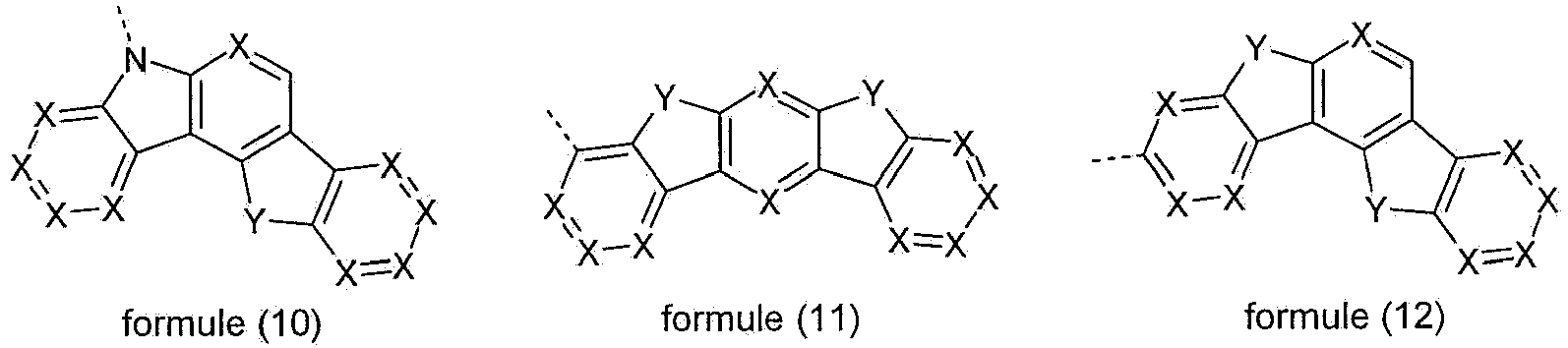


 X est pour chaque occurrence, de manière identique ou différente, CR1 ou N, où de préférence, un maximum de 2 symboles X par cycle représentent N ;Y est pour chaque occurrence, de manière identique ou différente, C(R1)2, NR1, O ou S ;n est 0 ou 1, où n égal à 0 signifie qu'aucun groupe Y n'est lié au niveau de cette position et qu'en lieu et place, des radicaux R1 sont liés aux atomes de carbone correspondants.
 - Dispositif électroluminescent organique selon la revendication 12,
caractérisé en ce que le matériau de transport d'électrons est sélectionné parmi les composés de la formule (45) ou (46) : E est, de manière identique ou différente pour chaque occurrence, une liaison simple, NR, CR2, O ou S ;Ar1 est, en association avec les atomes de carbone qui sont représentés de façon explicite, un système de cycle aromatique ou hétéroaromatique qui comporte de 5 à 30 atomes de cycle aromatique, lequel système de cycle peut être substitué par un radical ou par plusieurs radicaux R ;Ar2, Ar3 sont, de manière identique ou différente pour chaque occurrence, en association avec les atomes de carbone qui sont représentés de façon explicite, un système de cycle aromatique ou hétéroaromatique qui comporte de 5 à 30 atomes de cycle aromatique, lequel système de cycle peut être substitué par un radical ou par plusieurs radicaux R ;L est, pour m = 2, une liaison simple ou un groupe divalent, ou, pour m = 3, un groupe trivalent ou, pour m = 4, un groupe tétravalent, lequel groupe est dans chaque cas lié à Ar1, Ar2 ou Ar3 au niveau de n'importe quelle position souhaitée ou est lié à E en lieu et place d'un radical R ;m est 2, 3 ou 4.
 - Dispositif électroluminescent organique selon la revendication 15,
caractérisé en ce que le groupe Ar1 représente un groupe de la formule (47), (48), (49) ou (50), soit les formules qui suivent : W est, de manière identique ou différente pour chaque occurrence, CR ou N ; ou deux groupes adjacents W représentent un groupe de la formule (51) ou (52) :
 V est NR, O ou S;et/ou en ce que le groupe Ar2 représente un groupe de l'une des formules (53), (54) et (55) :
et/ou en ce que le groupe Ar3 représente un groupe de l'une des formules (56), (57), (58) et (59) :
* indique le lien sur E ou sur Ar2, et W et V présentent les significations qui ont été données ci-avant. - Dispositif électroluminescent organique selon la revendication 12, aractérisé en ce que le matériau de transport d'électrons est sélectionné parmi les composés des formules (70) et (71) :
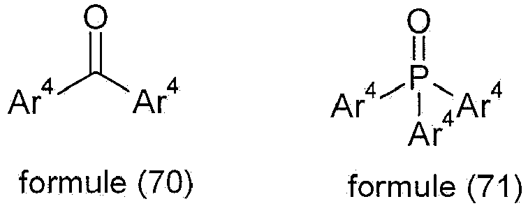 Ar4 est pour chaque occurrence, de manière identique ou différente, un système de cycle aromatique ou hétéroaromatique qui comporte de 5 à 80 atomes de cycle aromatique, de préférence jusqu'à 60 atomes de cycle aromatique, lequel système de cycle peut dans chaque cas être substitué par un ou par plusieurs groupe(s) R.
 - Procédé pour la production d'un dispositif électroluminescent organique selon une ou plusieurs des revendications 1 à 17, caractérisé en ce qu'au moins une couche est appliquée au moyen d'un procédé de sublimation et/ou en ce qu'au moins une couche est appliquée au moyen d'un procédé OVPD (dépôt organique en phase vapeur) ou à l'aide d'une sublimation à gaz porteur et/ou en ce qu'au moins une couche est appliquée à partir d'une solution, au moyen d'un dépôt/ revêtement à la tournette/par centrifugation ou au moyen d'un procédé d'impression.
Priority Applications (1)
| Application Number | Priority Date | Filing Date | Title |
|---|---|---|---|
| EP14711162.9A EP2984152B2 (fr) | 2013-04-08 | 2014-03-18 | Dispositif électroluminescent organique |
Applications Claiming Priority (3)
| Application Number | Priority Date | Filing Date | Title |
|---|---|---|---|
| EP13001796 | 2013-04-08 | ||
| EP14711162.9A EP2984152B2 (fr) | 2013-04-08 | 2014-03-18 | Dispositif électroluminescent organique |
| PCT/EP2014/000742 WO2014166586A1 (fr) | 2013-04-08 | 2014-03-18 | Dispositif électroluminescent organique |
Publications (3)
| Publication Number | Publication Date |
|---|---|
| EP2984152A1 EP2984152A1 (fr) | 2016-02-17 |
| EP2984152B1 true EP2984152B1 (fr) | 2018-04-25 |
| EP2984152B2 EP2984152B2 (fr) | 2022-01-05 |
Family
ID=48128050
Family Applications (1)
| Application Number | Title | Priority Date | Filing Date |
|---|---|---|---|
| EP14711162.9A Active EP2984152B2 (fr) | 2013-04-08 | 2014-03-18 | Dispositif électroluminescent organique |
Country Status (7)
| Country | Link |
|---|---|
| US (2) | US20160093812A1 (fr) |
| EP (1) | EP2984152B2 (fr) |
| JP (1) | JP6553022B2 (fr) |
| KR (1) | KR102177883B1 (fr) |
| CN (2) | CN111430557A (fr) |
| TW (1) | TWI661028B (fr) |
| WO (1) | WO2014166586A1 (fr) |
Families Citing this family (46)
| Publication number | Priority date | Publication date | Assignee | Title |
|---|---|---|---|---|
| US9847501B2 (en) | 2011-11-22 | 2017-12-19 | Idemitsu Kosan Co., Ltd. | Aromatic heterocyclic derivative, material for organic electroluminescent element, and organic electroluminescent element |
| EP3040335B1 (fr) | 2013-11-13 | 2019-04-03 | Idemitsu Kosan Co., Ltd | Composé, élément électroluminescent organique et dispositif électronique |
| EP3069392B1 (fr) | 2013-11-15 | 2019-08-07 | Merck Patent GmbH | Composé avec une nouvelle structure d'anneau à six éléments pour une utilisation dans des dispositifs électroniques organiques |
| US10734587B2 (en) * | 2014-03-13 | 2020-08-04 | Merck Patent Gmbh | Formulations of luminescent compounds |
| WO2016084962A1 (fr) | 2014-11-28 | 2016-06-02 | 出光興産株式会社 | Composé, matériau pour élément électroluminescent organique, élément électroluminescent organique et dispositif électronique |
| US9806269B2 (en) | 2014-12-05 | 2017-10-31 | Lg Display Co., Ltd. | Delayed fluorescence compound, and organic light emitting diode and display device using the same |
| WO2016091353A1 (fr) * | 2014-12-12 | 2016-06-16 | Merck Patent Gmbh | Composés organiques comprenant des groupes solubles |
| KR102343572B1 (ko) * | 2015-03-06 | 2021-12-28 | 삼성디스플레이 주식회사 | 유기 발광 소자 |
| GB201507340D0 (en) | 2015-04-29 | 2015-06-10 | Univ St Andrews | Light emitting devices and compounds |
| EP3305771B1 (fr) * | 2015-06-03 | 2021-12-01 | LG Chem, Ltd. | Dispositif électroluminescent organique contenant un composé hétérocyclique |
| KR102417039B1 (ko) * | 2015-08-20 | 2022-07-05 | 덕산네오룩스 주식회사 | 유기전기 소자용 화합물, 이를 이용한 유기전기소자 및 그 전자 장치 |
| KR102626916B1 (ko) | 2015-09-09 | 2024-01-19 | 삼성전자주식회사 | 축합환 화합물 및 이를 포함한 유기 발광 소자 |
| CN105418486A (zh) | 2015-12-25 | 2016-03-23 | 上海天马有机发光显示技术有限公司 | 有机电致发光化合物及其有机光电装置 |
| CN105418617B (zh) | 2015-12-25 | 2018-03-06 | 上海天马有机发光显示技术有限公司 | 有机电致发光化合物及其有机光电装置 |
| JP6788314B2 (ja) * | 2016-01-06 | 2020-11-25 | コニカミノルタ株式会社 | 有機エレクトロルミネッセンス素子、有機エレクトロルミネッセンス素子の製造方法、表示装置及び照明装置 |
| CN107056748B (zh) * | 2016-04-25 | 2020-12-11 | 中节能万润股份有限公司 | 一种以三嗪和酮为核心的化合物及其在有机电致发光器件上的应用 |
| JP6664514B2 (ja) * | 2016-05-10 | 2020-03-13 | エルジー・ケム・リミテッド | 有機電界発光素子およびその製造方法 |
| KR102651014B1 (ko) | 2016-05-26 | 2024-03-26 | 삼성디스플레이 주식회사 | 함질소 화합물 및 이를 포함하는 유기 전계 발광 소자 |
| EP3266772B1 (fr) * | 2016-07-06 | 2019-04-24 | Cynora Gmbh | Molécules organiques, en particulier destinées à être utilisées dans des composants optoélectroniques |
| JP6691848B2 (ja) * | 2016-07-21 | 2020-05-13 | 株式会社デンソー | 発光素子、表示装置および電子機器 |
| CN106206974B (zh) * | 2016-09-06 | 2018-03-23 | 苏州大学 | 热致延迟荧光有机电致发光体系以及使用该体系的发光二极管 |
| CN108023022B (zh) * | 2016-11-03 | 2020-07-14 | 上海和辉光电有限公司 | 一种有机电致发光器件及电子设备 |
| KR102754844B1 (ko) * | 2016-11-30 | 2025-01-15 | 삼성디스플레이 주식회사 | 다환 화합물 및 이를 포함하는 유기 전계 발광 소자 |
| KR102783283B1 (ko) | 2016-12-01 | 2025-03-20 | 삼성디스플레이 주식회사 | 방향족 화합물 및 이를 포함하는 유기 전계 발광 소자 |
| KR102817119B1 (ko) | 2017-01-19 | 2025-06-09 | 삼성디스플레이 주식회사 | 유기 전계 발광 소자 |
| KR102138823B1 (ko) * | 2017-12-27 | 2020-07-28 | 삼성에스디아이 주식회사 | 유기 광전자 소자 및 표시 장치 |
| CN109705126A (zh) * | 2018-06-29 | 2019-05-03 | 赛洛普(武汉)科技有限公司 | 一种用于有机电致发光器件的化合物及应用 |
| US12378197B2 (en) * | 2018-07-13 | 2025-08-05 | Universal Display Corporation | Organic electroluminescent materials and devices |
| KR102668688B1 (ko) | 2018-07-23 | 2024-05-24 | 삼성디스플레이 주식회사 | 유기 발광 소자 |
| CN111372918B (zh) | 2018-07-27 | 2023-09-05 | 出光兴产株式会社 | 化合物、用于有机电致发光元件的材料、有机电致发光元件以及电子设备 |
| WO2020061103A1 (fr) | 2018-09-18 | 2020-03-26 | Nikang Therapeutics, Inc. | Dérivés d'anneaux tricycliques fusionnés utilisés en tant qu'inhibiteurs de la phosphatase src à homologie-2 |
| KR102499281B1 (ko) | 2018-09-26 | 2023-02-13 | 가부시키가이샤 한도오따이 에네루기 켄큐쇼 | 발광 디바이스, 발광 장치, 전자 기기, 및 조명 장치 |
| TWI767148B (zh) | 2018-10-10 | 2022-06-11 | 美商弗瑪治療公司 | 抑制脂肪酸合成酶(fasn) |
| KR102622078B1 (ko) * | 2018-12-13 | 2024-01-05 | 엘지디스플레이 주식회사 | 유기발광다이오드 및 이를 포함하는 유기발광장치 |
| KR20200091979A (ko) | 2019-01-23 | 2020-08-03 | 삼성디스플레이 주식회사 | 유기 발광 소자 |
| KR102718897B1 (ko) | 2019-10-31 | 2024-10-16 | 삼성전자주식회사 | 발광 소자, 그 제조방법 및 이를 포함한 표시 장치 |
| CN110878062A (zh) * | 2019-11-27 | 2020-03-13 | 武汉华星光电半导体显示技术有限公司 | 热活化延迟荧光材料及其制备方法和电致发光器件 |
| WO2021191058A1 (fr) * | 2020-03-23 | 2021-09-30 | Merck Patent Gmbh | Matériaux pour dispositifs électroluminescents organiques |
| CN111635409B (zh) * | 2020-06-12 | 2021-10-12 | 欧洛德(武汉)光电科技有限公司 | 引入环状酰胺结构用于有机电致发光器件的化合物及应用 |
| CN111620883B (zh) * | 2020-06-12 | 2021-09-28 | 欧洛德(武汉)光电科技有限公司 | 一种用于有机电致发光器件的新型化合物 |
| CN111620882B (zh) * | 2020-06-12 | 2021-08-31 | 欧洛德(武汉)光电科技有限公司 | 新型用于有机电致发光器件的化合物及应用 |
| KR102493132B1 (ko) * | 2020-09-11 | 2023-01-31 | 삼성디스플레이 주식회사 | 발광 소자 및 이를 포함한 전자 장치 |
| KR20250111244A (ko) * | 2020-11-05 | 2025-07-22 | 이데미쓰 고산 가부시키가이샤 | 화합물, 유기 전기발광 소자용 재료, 유기 전기발광 소자 및 전자 기기 |
| US20220367826A1 (en) * | 2020-11-19 | 2022-11-17 | Boe Technology Group Co., Ltd. | Organic light-emitting diode and display panel |
| KR20240136308A (ko) * | 2022-01-21 | 2024-09-13 | 삼성디스플레이 주식회사 | 광전자 소자용 유기 분자 |
| CN117362292B (zh) * | 2023-06-15 | 2025-07-22 | 闽都创新实验室 | 酰胺衍生物热活化延迟荧光材料及其制备方法和应用 |
Citations (5)
| Publication number | Priority date | Publication date | Assignee | Title |
|---|---|---|---|---|
| US20120068170A1 (en) | 2009-05-29 | 2012-03-22 | Merck Patent Gmbh | Materials for organic electroluminescent devices |
| EP2511360A1 (fr) | 2009-12-07 | 2012-10-17 | Nippon Steel Chemical Co., Ltd. | Matière électroluminescente organique et élément électroluminescent organique |
| WO2013011955A1 (fr) | 2011-07-15 | 2013-01-24 | 国立大学法人九州大学 | Matériau à fluorescence retardée et élément d'électroluminescence organique utilisant ledit matériau |
| WO2013011954A1 (fr) * | 2011-07-15 | 2013-01-24 | 国立大学法人九州大学 | Élément d'électroluminescence organique et composé utilisé dans ledit élément |
| WO2013026515A1 (fr) | 2011-08-22 | 2013-02-28 | Merck Patent Gmbh | Dispositif électroluminescent organique |
Family Cites Families (14)
| Publication number | Priority date | Publication date | Assignee | Title |
|---|---|---|---|---|
| DE10357315A1 (de) * | 2003-12-05 | 2005-07-07 | Covion Organic Semiconductors Gmbh | Organisches Elektrolumineszenzelement |
| US20070013451A1 (en) * | 2004-04-21 | 2007-01-18 | Motorola, Inc. | Circuits for use in radio communications |
| EP1956022B1 (fr) * | 2005-12-01 | 2012-07-25 | Nippon Steel Chemical Co., Ltd. | Compose pour element electroluminescent organique et element electroluminescent organique |
| EP2080762B1 (fr) * | 2006-11-09 | 2016-09-14 | Nippon Steel & Sumikin Chemical Co., Ltd. | Composé pour un dispositif électroluminescent organique et dispositif électroluminescent organique |
| JP2009004491A (ja) * | 2007-06-20 | 2009-01-08 | Fujifilm Corp | 有機電界発光素子 |
| DE102008033943A1 (de) * | 2008-07-18 | 2010-01-21 | Merck Patent Gmbh | Neue Materialien für organische Elektrolumineszenzvorrichtungen |
| DE102009009277B4 (de) * | 2009-02-17 | 2023-12-07 | Merck Patent Gmbh | Organische elektronische Vorrichtung, Verfahren zu deren Herstellung und Verwendung von Verbindungen |
| JP5523060B2 (ja) * | 2009-03-16 | 2014-06-18 | キヤノン株式会社 | 新規ビクリセン化合物及びこれを有する有機発光素子 |
| DE102009031021A1 (de) * | 2009-06-30 | 2011-01-05 | Merck Patent Gmbh | Materialien für organische Elektrolumineszenzvorrichtungen |
| US8841655B2 (en) * | 2009-11-27 | 2014-09-23 | Sharp Kabushiki Kaisha | Organic electroluminescence element, manufacturing method thereof, and organic electroluminescence display device |
| US9487548B2 (en) * | 2009-12-14 | 2016-11-08 | Udc Ireland Limited | Metal complexes comprising diazabenzimidazolocarbene ligands and the use thereof in OLEDs |
| DE102010019306B4 (de) * | 2010-05-04 | 2021-05-20 | Merck Patent Gmbh | Organische Elektrolumineszenzvorrichtungen |
| DE102010027317A1 (de) * | 2010-07-16 | 2012-01-19 | Merck Patent Gmbh | Metallkomplexe |
| WO2012064987A1 (fr) * | 2010-11-11 | 2012-05-18 | Nitto Denko Corporation | Élément émetteur composite hybride et dispositifs électroluminescents l'utilisant |
-
2014
- 2014-03-18 US US14/782,621 patent/US20160093812A1/en not_active Abandoned
- 2014-03-18 WO PCT/EP2014/000742 patent/WO2014166586A1/fr not_active Ceased
- 2014-03-18 JP JP2016506801A patent/JP6553022B2/ja active Active
- 2014-03-18 KR KR1020157031343A patent/KR102177883B1/ko active Active
- 2014-03-18 CN CN202010151199.3A patent/CN111430557A/zh active Pending
- 2014-03-18 CN CN201480018014.4A patent/CN105102581A/zh active Pending
- 2014-03-18 EP EP14711162.9A patent/EP2984152B2/fr active Active
- 2014-04-03 TW TW103112539A patent/TWI661028B/zh not_active IP Right Cessation
-
2024
- 2024-09-13 US US18/884,179 patent/US20250008838A1/en active Pending
Patent Citations (7)
| Publication number | Priority date | Publication date | Assignee | Title |
|---|---|---|---|---|
| US20120068170A1 (en) | 2009-05-29 | 2012-03-22 | Merck Patent Gmbh | Materials for organic electroluminescent devices |
| EP2511360A1 (fr) | 2009-12-07 | 2012-10-17 | Nippon Steel Chemical Co., Ltd. | Matière électroluminescente organique et élément électroluminescent organique |
| WO2013011955A1 (fr) | 2011-07-15 | 2013-01-24 | 国立大学法人九州大学 | Matériau à fluorescence retardée et élément d'électroluminescence organique utilisant ledit matériau |
| WO2013011954A1 (fr) * | 2011-07-15 | 2013-01-24 | 国立大学法人九州大学 | Élément d'électroluminescence organique et composé utilisé dans ledit élément |
| EP2733762A1 (fr) * | 2011-07-15 | 2014-05-21 | Kyushu University, National University Corporation | Élément d'électroluminescence organique et composé utilisé dans ledit élément |
| EP2733761A1 (fr) | 2011-07-15 | 2014-05-21 | Kyushu University, National University Corporation | Matériau à fluorescence retardée et élément d'électroluminescence organique utilisant ledit matériau |
| WO2013026515A1 (fr) | 2011-08-22 | 2013-02-28 | Merck Patent Gmbh | Dispositif électroluminescent organique |
Non-Patent Citations (1)
| Title |
|---|
| HIROKI UOYAMA; GOUSHI KENICHI; SHIZU KATSUYUKI; NOMURA HIROKO; ADACHI CHIHAYA: "Highly efficient organic light-emitting diodes from delayed fluorescence", NATURE, vol. 492, 13 December 2012 (2012-12-13), pages 234 - 238, XP055048388 |
Also Published As
| Publication number | Publication date |
|---|---|
| EP2984152B2 (fr) | 2022-01-05 |
| JP2016514908A (ja) | 2016-05-23 |
| KR20150143552A (ko) | 2015-12-23 |
| US20250008838A1 (en) | 2025-01-02 |
| US20160093812A1 (en) | 2016-03-31 |
| TWI661028B (zh) | 2019-06-01 |
| KR102177883B1 (ko) | 2020-11-12 |
| WO2014166586A1 (fr) | 2014-10-16 |
| TW201506125A (zh) | 2015-02-16 |
| EP2984152A1 (fr) | 2016-02-17 |
| JP6553022B2 (ja) | 2019-07-31 |
| CN111430557A (zh) | 2020-07-17 |
| CN105102581A (zh) | 2015-11-25 |
Similar Documents
| Publication | Publication Date | Title |
|---|---|---|
| EP2984692B1 (fr) | Dispositif électroluminescent organique comportant une matière à fluorescence retardée thermiquement activée | |
| EP2984152B2 (fr) | Dispositif électroluminescent organique | |
| EP2984151B1 (fr) | Dispositif électroluminescent organique | |
| EP3005433B1 (fr) | Dispositif organique éléctroluminescent | |
| EP2907173B1 (fr) | Dispositif électronique | |
| EP2984691B1 (fr) | Dispositif émetteur de lumière organique à fluorescence retardée | |
| EP3117470B1 (fr) | Dispositif électroluminescent organique | |
| EP2695213B1 (fr) | Dispositif électroluminescent organique | |
| EP3044286B1 (fr) | Dispositif d'électroluminescence organique | |
| EP3460864B1 (fr) | Dispositifs électroniques | |
| DE112011102558B4 (de) | Organische Elektrolumineszenzvorrichtung | |
| EP2898042B1 (fr) | Matériaux pour dispositifs électroniques | |
| EP3210248B2 (fr) | Matériaux pour dispositifs électroniques | |
| EP2764558B1 (fr) | Dispositif électroluminescents organiques | |
| EP3120396B1 (fr) | Dispositif organique électroluminescent | |
| DE102009014513A1 (de) | Organische Elektrolumineszenzvorrichtung | |
| EP3887479B1 (fr) | Dispositif électronique | |
| EP4193399B1 (fr) | Dispositif électronique | |
| WO2020108899A1 (fr) | Dispositif électronique | |
| WO2021028513A1 (fr) | Dispositif électronique | |
| WO2011035835A1 (fr) | Dispositif électroluminescent organique | |
| EP3548485B1 (fr) | Matériaux pour dispositifs électroluminescents organiques | |
| EP4399952A1 (fr) | Dispositif électronique |
Legal Events
| Date | Code | Title | Description |
|---|---|---|---|
| PUAI | Public reference made under article 153(3) epc to a published international application that has entered the european phase |
Free format text: ORIGINAL CODE: 0009012 |
|
| 17P | Request for examination filed |
Effective date: 20150810 |
|
| AK | Designated contracting states |
Kind code of ref document: A1 Designated state(s): AL AT BE BG CH CY CZ DE DK EE ES FI FR GB GR HR HU IE IS IT LI LT LU LV MC MK MT NL NO PL PT RO RS SE SI SK SM TR |
|
| AX | Request for extension of the european patent |
Extension state: BA ME |
|
| DAX | Request for extension of the european patent (deleted) | ||
| 17Q | First examination report despatched |
Effective date: 20161007 |
|
| STAA | Information on the status of an ep patent application or granted ep patent |
Free format text: STATUS: EXAMINATION IS IN PROGRESS |
|
| RIC1 | Information provided on ipc code assigned before grant |
Ipc: C09K 11/06 20060101AFI20170412BHEP Ipc: H01L 51/56 20060101ALI20170412BHEP Ipc: H01L 33/00 20100101ALI20170412BHEP Ipc: H01L 27/32 20060101ALI20170412BHEP Ipc: H01L 51/00 20060101ALI20170412BHEP Ipc: H01L 51/50 20060101ALI20170412BHEP |
|
| GRAP | Despatch of communication of intention to grant a patent |
Free format text: ORIGINAL CODE: EPIDOSNIGR1 |
|
| STAA | Information on the status of an ep patent application or granted ep patent |
Free format text: STATUS: GRANT OF PATENT IS INTENDED |
|
| INTG | Intention to grant announced |
Effective date: 20171207 |
|
| GRAS | Grant fee paid |
Free format text: ORIGINAL CODE: EPIDOSNIGR3 |
|
| GRAA | (expected) grant |
Free format text: ORIGINAL CODE: 0009210 |
|
| STAA | Information on the status of an ep patent application or granted ep patent |
Free format text: STATUS: THE PATENT HAS BEEN GRANTED |
|
| AK | Designated contracting states |
Kind code of ref document: B1 Designated state(s): AL AT BE BG CH CY CZ DE DK EE ES FI FR GB GR HR HU IE IS IT LI LT LU LV MC MK MT NL NO PL PT RO RS SE SI SK SM TR |
|
| REG | Reference to a national code |
Ref country code: GB Ref legal event code: FG4D Free format text: NOT ENGLISH |
|
| REG | Reference to a national code |
Ref country code: CH Ref legal event code: EP |
|
| REG | Reference to a national code |
Ref country code: AT Ref legal event code: REF Ref document number: 992893 Country of ref document: AT Kind code of ref document: T Effective date: 20180515 |
|
| REG | Reference to a national code |
Ref country code: IE Ref legal event code: FG4D Free format text: LANGUAGE OF EP DOCUMENT: GERMAN |
|
| REG | Reference to a national code |
Ref country code: DE Ref legal event code: R096 Ref document number: 502014008070 Country of ref document: DE |
|
| REG | Reference to a national code |
Ref country code: NL Ref legal event code: MP Effective date: 20180425 |
|
| REG | Reference to a national code |
Ref country code: LT Ref legal event code: MG4D |
|
| PG25 | Lapsed in a contracting state [announced via postgrant information from national office to epo] |
Ref country code: NL Free format text: LAPSE BECAUSE OF FAILURE TO SUBMIT A TRANSLATION OF THE DESCRIPTION OR TO PAY THE FEE WITHIN THE PRESCRIBED TIME-LIMIT Effective date: 20180425 |
|
| PG25 | Lapsed in a contracting state [announced via postgrant information from national office to epo] |
Ref country code: FI Free format text: LAPSE BECAUSE OF FAILURE TO SUBMIT A TRANSLATION OF THE DESCRIPTION OR TO PAY THE FEE WITHIN THE PRESCRIBED TIME-LIMIT Effective date: 20180425 Ref country code: BG Free format text: LAPSE BECAUSE OF FAILURE TO SUBMIT A TRANSLATION OF THE DESCRIPTION OR TO PAY THE FEE WITHIN THE PRESCRIBED TIME-LIMIT Effective date: 20180725 Ref country code: NO Free format text: LAPSE BECAUSE OF FAILURE TO SUBMIT A TRANSLATION OF THE DESCRIPTION OR TO PAY THE FEE WITHIN THE PRESCRIBED TIME-LIMIT Effective date: 20180725 Ref country code: LT Free format text: LAPSE BECAUSE OF FAILURE TO SUBMIT A TRANSLATION OF THE DESCRIPTION OR TO PAY THE FEE WITHIN THE PRESCRIBED TIME-LIMIT Effective date: 20180425 Ref country code: SE Free format text: LAPSE BECAUSE OF FAILURE TO SUBMIT A TRANSLATION OF THE DESCRIPTION OR TO PAY THE FEE WITHIN THE PRESCRIBED TIME-LIMIT Effective date: 20180425 Ref country code: PL Free format text: LAPSE BECAUSE OF FAILURE TO SUBMIT A TRANSLATION OF THE DESCRIPTION OR TO PAY THE FEE WITHIN THE PRESCRIBED TIME-LIMIT Effective date: 20180425 Ref country code: ES Free format text: LAPSE BECAUSE OF FAILURE TO SUBMIT A TRANSLATION OF THE DESCRIPTION OR TO PAY THE FEE WITHIN THE PRESCRIBED TIME-LIMIT Effective date: 20180425 |
|
| PG25 | Lapsed in a contracting state [announced via postgrant information from national office to epo] |
Ref country code: LV Free format text: LAPSE BECAUSE OF FAILURE TO SUBMIT A TRANSLATION OF THE DESCRIPTION OR TO PAY THE FEE WITHIN THE PRESCRIBED TIME-LIMIT Effective date: 20180425 Ref country code: RS Free format text: LAPSE BECAUSE OF FAILURE TO SUBMIT A TRANSLATION OF THE DESCRIPTION OR TO PAY THE FEE WITHIN THE PRESCRIBED TIME-LIMIT Effective date: 20180425 Ref country code: HR Free format text: LAPSE BECAUSE OF FAILURE TO SUBMIT A TRANSLATION OF THE DESCRIPTION OR TO PAY THE FEE WITHIN THE PRESCRIBED TIME-LIMIT Effective date: 20180425 Ref country code: GR Free format text: LAPSE BECAUSE OF FAILURE TO SUBMIT A TRANSLATION OF THE DESCRIPTION OR TO PAY THE FEE WITHIN THE PRESCRIBED TIME-LIMIT Effective date: 20180726 |
|
| PG25 | Lapsed in a contracting state [announced via postgrant information from national office to epo] |
Ref country code: PT Free format text: LAPSE BECAUSE OF FAILURE TO SUBMIT A TRANSLATION OF THE DESCRIPTION OR TO PAY THE FEE WITHIN THE PRESCRIBED TIME-LIMIT Effective date: 20180827 |
|
| REG | Reference to a national code |
Ref country code: DE Ref legal event code: R026 Ref document number: 502014008070 Country of ref document: DE |
|
| PG25 | Lapsed in a contracting state [announced via postgrant information from national office to epo] |
Ref country code: EE Free format text: LAPSE BECAUSE OF FAILURE TO SUBMIT A TRANSLATION OF THE DESCRIPTION OR TO PAY THE FEE WITHIN THE PRESCRIBED TIME-LIMIT Effective date: 20180425 Ref country code: SK Free format text: LAPSE BECAUSE OF FAILURE TO SUBMIT A TRANSLATION OF THE DESCRIPTION OR TO PAY THE FEE WITHIN THE PRESCRIBED TIME-LIMIT Effective date: 20180425 Ref country code: DK Free format text: LAPSE BECAUSE OF FAILURE TO SUBMIT A TRANSLATION OF THE DESCRIPTION OR TO PAY THE FEE WITHIN THE PRESCRIBED TIME-LIMIT Effective date: 20180425 Ref country code: CZ Free format text: LAPSE BECAUSE OF FAILURE TO SUBMIT A TRANSLATION OF THE DESCRIPTION OR TO PAY THE FEE WITHIN THE PRESCRIBED TIME-LIMIT Effective date: 20180425 Ref country code: RO Free format text: LAPSE BECAUSE OF FAILURE TO SUBMIT A TRANSLATION OF THE DESCRIPTION OR TO PAY THE FEE WITHIN THE PRESCRIBED TIME-LIMIT Effective date: 20180425 |
|
| PLBI | Opposition filed |
Free format text: ORIGINAL CODE: 0009260 |
|
| PLAX | Notice of opposition and request to file observation + time limit sent |
Free format text: ORIGINAL CODE: EPIDOSNOBS2 |
|
| PG25 | Lapsed in a contracting state [announced via postgrant information from national office to epo] |
Ref country code: SM Free format text: LAPSE BECAUSE OF FAILURE TO SUBMIT A TRANSLATION OF THE DESCRIPTION OR TO PAY THE FEE WITHIN THE PRESCRIBED TIME-LIMIT Effective date: 20180425 Ref country code: IT Free format text: LAPSE BECAUSE OF FAILURE TO SUBMIT A TRANSLATION OF THE DESCRIPTION OR TO PAY THE FEE WITHIN THE PRESCRIBED TIME-LIMIT Effective date: 20180425 |
|
| 26 | Opposition filed |
Opponent name: NIPPON STEEL CHEMICAL & MATERIAL CO., LTD. Effective date: 20190125 |
|
| PG25 | Lapsed in a contracting state [announced via postgrant information from national office to epo] |
Ref country code: SI Free format text: LAPSE BECAUSE OF FAILURE TO SUBMIT A TRANSLATION OF THE DESCRIPTION OR TO PAY THE FEE WITHIN THE PRESCRIBED TIME-LIMIT Effective date: 20180425 |
|
| PLAF | Information modified related to communication of a notice of opposition and request to file observations + time limit |
Free format text: ORIGINAL CODE: EPIDOSCOBS2 |
|
| PLBB | Reply of patent proprietor to notice(s) of opposition received |
Free format text: ORIGINAL CODE: EPIDOSNOBS3 |
|
| PG25 | Lapsed in a contracting state [announced via postgrant information from national office to epo] |
Ref country code: MC Free format text: LAPSE BECAUSE OF FAILURE TO SUBMIT A TRANSLATION OF THE DESCRIPTION OR TO PAY THE FEE WITHIN THE PRESCRIBED TIME-LIMIT Effective date: 20180425 |
|
| REG | Reference to a national code |
Ref country code: CH Ref legal event code: PL |
|
| GBPC | Gb: european patent ceased through non-payment of renewal fee |
Effective date: 20190318 |
|
| PG25 | Lapsed in a contracting state [announced via postgrant information from national office to epo] |
Ref country code: LU Free format text: LAPSE BECAUSE OF NON-PAYMENT OF DUE FEES Effective date: 20190318 Ref country code: AL Free format text: LAPSE BECAUSE OF FAILURE TO SUBMIT A TRANSLATION OF THE DESCRIPTION OR TO PAY THE FEE WITHIN THE PRESCRIBED TIME-LIMIT Effective date: 20180425 |
|
| REG | Reference to a national code |
Ref country code: BE Ref legal event code: MM Effective date: 20190331 |
|
| PG25 | Lapsed in a contracting state [announced via postgrant information from national office to epo] |
Ref country code: GB Free format text: LAPSE BECAUSE OF NON-PAYMENT OF DUE FEES Effective date: 20190318 Ref country code: CH Free format text: LAPSE BECAUSE OF NON-PAYMENT OF DUE FEES Effective date: 20190331 Ref country code: LI Free format text: LAPSE BECAUSE OF NON-PAYMENT OF DUE FEES Effective date: 20190331 Ref country code: IE Free format text: LAPSE BECAUSE OF NON-PAYMENT OF DUE FEES Effective date: 20190318 |
|
| PG25 | Lapsed in a contracting state [announced via postgrant information from national office to epo] |
Ref country code: FR Free format text: LAPSE BECAUSE OF NON-PAYMENT OF DUE FEES Effective date: 20190331 Ref country code: BE Free format text: LAPSE BECAUSE OF NON-PAYMENT OF DUE FEES Effective date: 20190331 |
|
| PG25 | Lapsed in a contracting state [announced via postgrant information from national office to epo] |
Ref country code: TR Free format text: LAPSE BECAUSE OF FAILURE TO SUBMIT A TRANSLATION OF THE DESCRIPTION OR TO PAY THE FEE WITHIN THE PRESCRIBED TIME-LIMIT Effective date: 20180425 |
|
| PG25 | Lapsed in a contracting state [announced via postgrant information from national office to epo] |
Ref country code: MT Free format text: LAPSE BECAUSE OF FAILURE TO SUBMIT A TRANSLATION OF THE DESCRIPTION OR TO PAY THE FEE WITHIN THE PRESCRIBED TIME-LIMIT Effective date: 20180425 |
|
| PLAY | Examination report in opposition despatched + time limit |
Free format text: ORIGINAL CODE: EPIDOSNORE2 |
|
| REG | Reference to a national code |
Ref country code: AT Ref legal event code: MM01 Ref document number: 992893 Country of ref document: AT Kind code of ref document: T Effective date: 20190318 |
|
| PLBC | Reply to examination report in opposition received |
Free format text: ORIGINAL CODE: EPIDOSNORE3 |
|
| PG25 | Lapsed in a contracting state [announced via postgrant information from national office to epo] |
Ref country code: AT Free format text: LAPSE BECAUSE OF NON-PAYMENT OF DUE FEES Effective date: 20190318 |
|
| PG25 | Lapsed in a contracting state [announced via postgrant information from national office to epo] |
Ref country code: CY Free format text: LAPSE BECAUSE OF FAILURE TO SUBMIT A TRANSLATION OF THE DESCRIPTION OR TO PAY THE FEE WITHIN THE PRESCRIBED TIME-LIMIT Effective date: 20180425 |
|
| PG25 | Lapsed in a contracting state [announced via postgrant information from national office to epo] |
Ref country code: IS Free format text: LAPSE BECAUSE OF FAILURE TO SUBMIT A TRANSLATION OF THE DESCRIPTION OR TO PAY THE FEE WITHIN THE PRESCRIBED TIME-LIMIT Effective date: 20180825 |
|
| PG25 | Lapsed in a contracting state [announced via postgrant information from national office to epo] |
Ref country code: HU Free format text: LAPSE BECAUSE OF FAILURE TO SUBMIT A TRANSLATION OF THE DESCRIPTION OR TO PAY THE FEE WITHIN THE PRESCRIBED TIME-LIMIT; INVALID AB INITIO Effective date: 20140318 |
|
| PUAH | Patent maintained in amended form |
Free format text: ORIGINAL CODE: 0009272 |
|
| STAA | Information on the status of an ep patent application or granted ep patent |
Free format text: STATUS: PATENT MAINTAINED AS AMENDED |
|
| 27A | Patent maintained in amended form |
Effective date: 20220105 |
|
| AK | Designated contracting states |
Kind code of ref document: B2 Designated state(s): AL AT BE BG CH CY CZ DE DK EE ES FI FR GB GR HR HU IE IS IT LI LT LU LV MC MK MT NL NO PL PT RO RS SE SI SK SM TR |
|
| REG | Reference to a national code |
Ref country code: DE Ref legal event code: R102 Ref document number: 502014008070 Country of ref document: DE |
|
| PG25 | Lapsed in a contracting state [announced via postgrant information from national office to epo] |
Ref country code: MK Free format text: LAPSE BECAUSE OF FAILURE TO SUBMIT A TRANSLATION OF THE DESCRIPTION OR TO PAY THE FEE WITHIN THE PRESCRIBED TIME-LIMIT Effective date: 20180425 |
|
| P01 | Opt-out of the competence of the unified patent court (upc) registered |
Effective date: 20230518 |
|
| PGFP | Annual fee paid to national office [announced via postgrant information from national office to epo] |
Ref country code: DE Payment date: 20260219 Year of fee payment: 13 |