EP2985932B1 - Sous-système d'émission optique multi-porteuses, et procédé de génération d'un signal optique - Google Patents
Sous-système d'émission optique multi-porteuses, et procédé de génération d'un signal optique Download PDFInfo
- Publication number
- EP2985932B1 EP2985932B1 EP13881480.1A EP13881480A EP2985932B1 EP 2985932 B1 EP2985932 B1 EP 2985932B1 EP 13881480 A EP13881480 A EP 13881480A EP 2985932 B1 EP2985932 B1 EP 2985932B1
- Authority
- EP
- European Patent Office
- Prior art keywords
- microring
- modulators
- light
- modulator
- light source
- Prior art date
- Legal status (The legal status is an assumption and is not a legal conclusion. Google has not performed a legal analysis and makes no representation as to the accuracy of the status listed.)
- Active
Links
Images


Classifications
-
- H—ELECTRICITY
- H04—ELECTRIC COMMUNICATION TECHNIQUE
- H04B—TRANSMISSION
- H04B10/00—Transmission systems employing electromagnetic waves other than radio-waves, e.g. infrared, visible or ultraviolet light, or employing corpuscular radiation, e.g. quantum communication
- H04B10/50—Transmitters
- H04B10/501—Structural aspects
- H04B10/506—Multiwavelength transmitters
Definitions
- the present invention relates to optical communications technologies, and in particular, to a multicarrier-based optical transmit subsystem and a method for generating an optical signal.
- optical transceiver assemblies With the development of the optical communications industry, technologies related to optical transceiver assemblies also continuously evolve, and an optical assembly that has a high speed, a low cost, and low power consumption and is miniaturized gradually attracts more attention in the industry.
- a WDM light source for example, a multichannel optical transmit device with different wavelengths, or a comb-shaped light source may be directly used as the WDM light source.
- a comb-shaped light source includes basic components such as a frequency shifter, a band-pass filter, an optical amplifier, and a coupler, and implements output of polychromatic light with a comb-shaped spectrum.
- a modulation signal is loaded by using polychromatic light with a comb-shaped spectrum, where the polychromatic light with a comb-shaped spectrum is output by a comb-shaped light source
- light generated by the comb-shaped light source is first split by using a demultiplexer, to obtain multiple beams of single-frequency light (that is, to obtain different beams of monochromatic light) or multiple single-frequency optical carriers, then the modulation signal is loaded to each of the different beams of monochromatic light, to obtain multiple optical signals with different frequencies, and then the multiple optical signals with different frequencies are multiplexed and output by using a wavelength division multiplexer.
- this solution has many disadvantages, for example, beams of light with a comb-shaped spectrum are simultaneously generated by using a feedback loop, and in a process in which the light with a comb-shaped spectrum is used as an optical carrier, the light needs to be split and modulated by using a demultiplexer and then multiplexed by using a wavelength division multiplexer, and therefore, an implementation process is complex.
- CHRISTOPHER NITTA ET AL "DCOF An Arbitration Free Directly Connected Optical Fabric" IEEE JOURNAL ON EMERGING AND SELECTED TOPICS IN CIRCUITS AND SYSTEMS, IEEE, PISCATAWAY, NJ, USA, vol. 2, no. 2, doi:10.1109/JETCAS.2012.2193842, ISSN 2156-3357, PAGE 169 - 182 , discloses an optical modulator connected to an optical detector via a single waveguide.
- the optical modulator and the optical detector may comprise a plurality of microring resonators.
- LINJIE ZHOU ET AL "Towards athermal optically-interconnected computing system using slotted silicon microring resonators and RF-photonic comb generation", APPLIED PHYSICS A; MATERIALS SCIENCE & PROCESSING, SPRINGER, BERLIN, DE, vol. 95, no. 4, ISSN 1432-0630, PAGE 1101 - 1109 , discloses a dual electrode Mach-Zehender modulator connected to a spectrum measurement via a single mode optical fibre (SMF-28).
- SMF-28 single mode optical fibre
- DONG PO ET AL "Low-power photonic components for optical interconnects", OPTOELECTRONIC INTERCONNECTS AND COMPONENT INTEGRATION XI, SPIE, 1000 20TH ST. BELLINGHAM WA 98225-6705 USA, (20110210), vol. 7944, no. 1, doi:10.1117/12.876425, PAGE 1 - 8 , shows a microring modulator connected to a microring detector via a single link.
- embodiments of the present invention provide a multicarrier-based optical transmit subsystem and a method for generating an optical signal, so as to simplify a structure of the multicarrier-based optical transmit subsystem.
- an embodiment of the present invention provides a multi-carrier-based optical transmit subsystem, including:
- the frequency shifting apparatus is a phase modulator to which a microwave signal is loaded, the same microwave signals are loaded to the phase modulators.
- an optical amplifier is connected between any two adjacent frequency shifting apparatuses.
- system further includes:
- an embodiment of the present invention provides a method for generating an optical signal, including:
- the outputting multiple optical signals among the optical signals with different frequencies to the plurality of public waveguide further includes:
- the method further includes:
- optical signals with different frequencies are obtained by filtering and modulating polychromatic light by using a microring group, and are output to a public waveguide by using respective download ends of microring modulators.
- the polychromatic light can be split, and a modulation signal is loaded to optical carriers obtained by means of filtering, to obtain the optical signals with different frequencies; in addition, by connecting the download ends of the microring modulators in the microring group to the public waveguide, the optical signals with different frequencies that are obtained by means of modulation are multiplexed in the public waveguide, so that an extra demultiplexer and wavelength division multiplexer do not need to be disposed in a multicarrier-based optical transmit subsystem, and a structure of the multicarrier-based optical transmit subsystem is simplified, thereby reducing a cost of the multicarrier-based optical transmit subsystem.
- FIG. 1 is a schematic diagram of a multicarrier-based optical transmit subsystem according to an embodiment of the present invention.
- the system includes: a comb-shaped light source apparatus 11, a microring group 12, and a public waveguide 13.
- the comb-shaped light source apparatus 11 is configured to generate and output polychromatic light, such as light with a comb-shaped spectrum.
- the microring group 12 includes multiple microring modulators, where each of the multiple microring modulators includes an input end and a download end, the input end of each of the multiple microring modulators is connected to the comb-shaped light source apparatus, and the multiple microring modulators each are configured to filter and modulate the polychromatic light, to obtain optical signals with different frequencies, and output the optical signals by using respective download ends of the microring modulators.
- the microring group 12 includes five microring modulators, and each microring modulators responds to one beam of monochromatic light or light with one frequency.
- the polychromatic light generated by the comb-shaped light source apparatus 11 includes light whose frequency is f1 (hereinafter referred to as light f1), light whose frequency is f2 (hereinafter referred to as light f2), light whose frequency is f3 (hereinafter referred to as light f3), light whose frequency is f4 (hereinafter referred to as light f4), and light whose frequency is f5 (hereinafter referred to as light f5)
- different microring modulators in the microring group 12 respectively respond to the five beams of monochromatic light.
- the microring group 12 has a microring modulator W1, a microring modulator W2, a microring modulator W3, a microring modulator W4, and a microring modulator W5, the microring modulator W1 responds to the light f1, the microring modulator W2 responds to the light f2, the microring modulator W3 responds to the light f3, the microring modulator W4 responds to the light f4, and the microring modulator W5 responds to the light f5.
- Responding to light with one frequency means filtering out light with all other frequencies in a free spectral range except the light, and using the light with the frequency to which a microring modulator responds as an optical carrier, to load a modulation signal, that is, to perform modulation to obtain an optical signal with the frequency.
- the microring modulator W1 responds to the light f1, that is, filters out light with other frequencies in a free spectral range except the light f1 and loads a modulation signal by using the light f1, to obtain an optical signal whose frequency is f1.
- the microring modulator W2 outputs an optical signal whose frequency is f2
- the microring modulator W3 outputs an optical signal whose frequency is f3
- the microring modulator W4 outputs an optical signal whose frequency is f4
- the microring modulator W5 outputs an optical signal whose frequency is f5.
- the microring modulators each output the optical signal by using respective download ends of the microring modulators.
- microring modulators each respond to light with one frequency, so that the polychromatic light can be split, and a modulation signal can be loaded to optical carriers obtained by means of filtering, to obtain optical signals; in this way, using of a demultiplexer is avoided, and a structure of the multicarrier-based optical transmit subsystem is simplified, thereby reducing a cost of the multicarrier-based optical transmit subsystem and making generating of an optical signal more convenient and efficient.
- the public waveguide 13 is connected to the download ends of the multiple microring modulators, and is configured to multiplex all or some optical signals among the optical signals with different frequencies.
- a download end of each of the microring modulator W1, the microring modulator W2, the microring modulator W3, the microring modulator W4, and the microring modulator W5 is connected to the public waveguide 13, and optical signals with at least five frequencies of f1, f2, f3, f4, and f5 are mixed together in the public waveguide 13, that is, multiplexing is implemented; in this way, using of a wavelength division multiplexer is avoided, and the structure of the multicarrier-based optical transmit subsystem is further simplified, thereby reducing a cost of the multicarrier-based optical transmit subsystem and making generating of an optical signal more convenient and efficient.
- the multicarrier-based optical transmit subsystem may have one or multiple channels of output and a signal of each channel is output by using a public waveguide.
- each of the download ends of all the microring modulators in the microring group 12 is connected to the public waveguide 13.
- microring modulators in the microring group 12 are grouped into multiple microring subgroups whose quantity is the same as that of the public waveguides 13, and the microring subgroups are connected to the public waveguides 13 in a one-to-one correspondence manner.
- the microring modulator W1, the microring modulator W2, the microring modulator W3, the microring modulator W4, and the microring modulator W5 are still used as an example.
- the microring modulator W1, the microring modulator W2, the microring modulator W3, the microring modulator W4, and the microring modulator W5 are grouped into two microring subgroups G1 and G2, where the microring subgroup G1 includes the microring modulator W1 and the microring modulator W2, and the microring subgroup G2 includes the microring modulator W3, the microring modulator W4, and the microring modulator W5.
- the download ends of the microring modulator W1 and the microring modulator W2 in the microring subgroup G1 is connected to one of the public waveguides 13, to implement multiplexing of the optical signals whose frequencies are f1 and f2.
- Each of the download ends of the microring modulator W3, the microring modulator W4, and the microring modulator W5 in the microring subgroup G2 is connected to the other public waveguide 13, to implement multiplexing of the optical signals whose frequencies are f3, f4, and f5.
- the comb-shaped light source apparatus may include one light source and at least one frequency shifting apparatus, where the at least one frequency shifting apparatus is connected to the light source, and is configured to perform frequency shifting on light emitted by the light source, to obtain polychromatic light, so that the multicarrier-based optical transmit subsystem can generate the polychromatic light without a feedback loop, and the structure of the multicarrier-based optical transmit subsystem is further simplified, thereby reducing a cost of the multicarrier-based optical transmit subsystem and making generating of an optical signal more convenient and efficient.
- each of the microring modulators in the microring group 12 is connected to a first waveguide, and the first waveguide is connected to an output end of the frequency shifting apparatus.
- a quantity of the microring modulators in the microring group 12 is equal to or greater than a quantity of the frequency shifting apparatuses
- the frequency shifting apparatuses are connected in series by using a second waveguide, an output end of a frequency shifting apparatus that is farthest from the light source is connected to a third waveguide, and the third waveguide and each second waveguide each are connected to at least one microring modulator in the microring group 12.
- the frequency shifting apparatus may be a frequency shifter or may be a phase modulator.
- the frequency shifting apparatus is a phase modulator, a microwave signal is loaded to the phase modulator, and when there are multiple frequency shifting apparatuses, the same microwave signals are loaded to the phase modulators.
- an optical amplifier may be connected between any two adjacent frequency shifting apparatuses, so as to ensure that the polychromatic light has enough energy to be transmitted backwards.
- multicarrier-based optical transmit subsystem provided in this embodiment of the present invention may further include:
- optical signals with different frequencies are obtained by filtering and modulating polychromatic light by using a microring group, and are output to a public waveguide by using respective download ends of microring modulators.
- the polychromatic light can be split, and a modulation signal is loaded to optical carriers obtained by means of filtering, to obtain the optical signals with different frequencies; in addition, by connecting the download ends of the microring modulators in the microring group to the public waveguide, the optical signals that with different frequencies that are obtained by means of modulation are multiplexed in the public waveguide, so that an extra demultiplexer and wavelength division multiplexer do not need to be disposed in a multicarrier-based optical transmit subsystem, and a structure of the multicarrier-based optical transmit subsystem is simplified, thereby reducing a cost of the multicarrier-based optical transmit subsystem.
- frequency shifting may be performed on a seed light source stage by stage, to generate a light source with multiple wavelengths; then a single-wavelength light source is obtained by means of filtering by a filter, and a modulation signal is loaded; and then for multiple channels on which the signals are loaded, wavelength division multiplexing is performed on the signals that are loaded on the multiple channels, and the signals that are loaded on the multiple channels and on which the wavelength division multiplexing has been performed are output.
- frequency shifting may be performed on a seed light source stage by stage, to generate a light source with multiple wavelengths; then a single-wavelength light source is obtained by means of filtering by a filter, and a modulation signal is loaded; and then for multiple channels on which the signals are loaded, wavelength division multiplexing is performed on the signals that are loaded on the multiple channels, and the signals that are loaded on the multiple channels and on which the wavelength division multiplexing has been performed are output.
- FIG. 2 is a flowchart of a method for generating an optical signal according to another embodiment of the present invention.
- the method shown in this embodiment can be implemented by using the system shown in FIG. 1 , and includes:
- the generating and outputting polychromatic light by using one light source may include:
- the generating and outputting polychromatic light by using one light source may include:
- the outputting multiple optical signals among the optical signals with different frequencies to a public waveguide may further include:
- the method for generating an optical signal may further include:
- optical signals with different frequencies are obtained by filtering and modulating polychromatic light by using multiple modulators, and are output to a public waveguide by using respective download ends of the microring modulators.
- the polychromatic light can be split, and a modulation signal is loaded to optical carriers obtained by means of filtering, to obtain the optical signals with different frequencies;
- the download ends of the microring modulators in the microring group to the public waveguide, the optical signals with different frequencies that are obtained by means of modulation are multiplexed in the public waveguide, so that an extra demultiplexer and wavelength division multiplexer do not need to be disposed in a multicarrier-based optical transmit subsystem, and a structure of the multicarrier-based optical transmit subsystem is simplified, thereby reducing a cost of the multicarrier-based optical transmit subsystem.
- frequency shifting may be performed on a seed light source stage by stage, to generate light source of multiple wavelengths, then a single-wavelength light source is obtained through filtering by a filter and a modulation signal is loaded, and then for multiple channels on which the signals are loaded, wavelength division multiplexing is performed on the signals that are loaded on the multiple channels, and the signals that are loaded on the multiple channels and on which the wavelength division multiplexing has been performed are output.
- a seed light source stage by stage to generate light source of multiple wavelengths
- a single-wavelength light source is obtained through filtering by a filter and a modulation signal is loaded
- wavelength division multiplexing is performed on the signals that are loaded on the multiple channels
- the signals that are loaded on the multiple channels and on which the wavelength division multiplexing has been performed are output.
- FIG. 3 is a schematic structural diagram of a multicarrier-based optical transmit subsystem according to another embodiment of the present invention.
- This embodiment is similar to the embodiment shown in FIG. 1 , and a difference lies in that a comb-shaped light source apparatus in this embodiment includes one light source and multiple frequency shifting apparatuses, the frequency shifting apparatuses are phase modulators, and a same microwave signal is loaded to each phase modulator.
- FIG. 3 shows two phase modulators and two microring modulators.
- the two phase modulators are cascaded, a same microwave signal is loaded to the two phase modulators, and each phase modulator is connected to one microring modulator.
- a light source 31 generates an optical signal whose central frequency is f 0 .
- an external microwave signal source loads a signal V m sin(2 ⁇ f s t) and a signal V m cos(2 ⁇ f s t) to two arms of the first phase modulator 32 respectively.
- V m sin(2 ⁇ f s t) a signal V m cos(2 ⁇ f s t) to two arms of the first phase modulator 32 respectively.
- a process of generating an optical signal on a first channel is used as an example.
- the polychromatic light obtained after frequency shifting is transmitted along a waveguide 38 (that is, the second waveguide in the embodiment shown in FIG. 1 ), and enters a straight waveguide of a first microring modulator 34 after being coupled by a coupling waveguide 33, and then is coupled and enters a ring waveguide.
- the to-be-transmitted signal is from a first signal source.
- the polychromatic light with a comb-shaped spectrum after frequency shifting that is output by the first phase modulator 32 enters a second phase modulator 35. Because a same microwave signal from a same microwave signal source is loaded to the second phase modulator 35 and the first phase modulator 32, a generated frequency shifting effect is similar.
- the second microring modulator 37 is connected to a waveguide 39 (that is, the third waveguide in the embodiment shown in FIG. 1 ), and polychromatic light output by the second phase modulator 35 is obtained by using a coupling waveguide 36.
- a third-stage channel, a fourth-stage channel, and even more channels may be further configured. Accordingly, a third phase modulator, a fourth phase modulator, a third microring modulator, a fourth microring modulator, and even more microring modulators may be further configured.
- a quantity of phase modulators may be equal to or less than a quantity of channels
- a quantity of microring modulators is equal to a quantity of channels
- a connection manner is similar to that shown in FIG. 3 .
- a waveguide to which an output end of one phase modulator is connected may be connected to two or more microring modulators.
- An optical amplifier 310 is a candidate device, and is connected between two phase modulators. After being coupled by multiple coupling waveguides, optical power of polychromatic light transmitted on a waveguide has a certain degree of loss, and the optical amplifier 310 may be configured to increase optical power of the polychromatic light with the comb-shaped spectrum.
- composition of waveguides of microring modulators such as the microring modulator 34 and the microring modulator 37 may be shown in FIG. 4 , and the composition of waveguides of microring modulators includes a straight waveguide 41, a straight waveguide 42, and a ring waveguide 43.
- One end of the straight waveguide 41 is an input end (that is, a port 1), and the other end is a straight-through end (that is, a port 2).
- One end of the straight waveguide 42 is an upload end (that is, a port 3), and the other end is a download end (that is, a port 4).
- each microring modulator After obtaining an optical signal by means of modulation, each microring modulator outputs the optical signal obtained by means of modulation to a channel by using a download end.
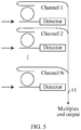
- Optical signals on channels are multiplexed and output by using a public waveguide.
- a download end of a first microring modulator is connected to a public waveguide 51 by using a channel 1
- a download end of a second microring modulator is connected to the public waveguide 51 by using a channel 2.
- a download end of an N th microring modulator is connected to the public waveguide 51 by using a channel N.
- optical signals with different frequencies are multiplexed and output by using the public waveguide 51 without a need for introducing an extra optical wavelength division multiplexer, and a structure of a multicarrier-based optical transmit subsystem is simplified, thereby reducing a cost.
- a straight-through end of a microring modulator may be used as a port for optoelectronic monitoring, that is, an optoelectronic detector for monitoring the outside, to monitor, in real time, a parameter of an optical signal passing through the microring modulator.
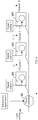
- FIG. 6 is a schematic structural diagram of a multicarrier-based optical transmit subsystem according to another embodiment of the present invention. This embodiment is similar to the embodiment shown in FIG. 3 , and relative strength between a central frequency and a side lobe can be controlled by adjusting a working point of a phase modulator. A difference lies in that there is one frequency shifting apparatus in this embodiment, which is applicable to an application scenario in which there are fewer channels.
- a microring group includes N microring modulators: a microring modulator 631, a microring modulator 632, ..., and a microring modulator 63N, each of which filters and modulates the polychromatic light with the comb-shaped spectrum, to load N different modulation signals to light with different frequencies in the polychromatic light and then output the light to a public waveguide through N channels: a channel 1, a channel 2, ..., and a channel N (for details, refer to FIG. 5 ), so as to implement multiplexing output.
- the N different modulation signals are from N signal sources: a signal source 1, a signal source 2, ..., and a signal source N.
- microring modulators may also be monitored, and a monitoring manner is the same as that in the descriptions in the embodiment shown in FIG. 3 , which is not described again.
- a dot-frequency signal provided by a microwave signal source frequency shifting of a light source is implemented, so as to generate multi-carrier output, that is, polychromatic light with a comb-shaped spectrum; then microring modulators filter and modulate the polychromatic light obtained by mean of frequency shifting, to obtain optical signals with different frequencies; and by using features of the microring modulators, a download end of each of the microring modulators is connected to a public waveguide, to multiplex the optical signals with different frequencies.
- the foregoing embodiment is applicable to a WDM optical transmit scenario in which there are few channels. Because microring modulators used for filtering and modulating are introduced, and download ends of the microring modulators are connected to a public waveguide to implement multiplexing, the multicarrier-based optical transmit subsystem provided in the embodiment of the present invention has advantages of a simple and compact structure, easy integration, and the like.
- the optical signal transmit subsystem provided in the embodiment of the present invention has advantages of a simpler structure and a more flexible configuration in an application scenario in which a quantity of channels is changeable.
Landscapes
- Engineering & Computer Science (AREA)
- Computer Networks & Wireless Communication (AREA)
- Signal Processing (AREA)
- Physics & Mathematics (AREA)
- Electromagnetism (AREA)
- Optical Modulation, Optical Deflection, Nonlinear Optics, Optical Demodulation, Optical Logic Elements (AREA)
- Optical Communication System (AREA)
Claims (7)
- Sous-système de transmission optique multiporteuse, comprenant :un appareil source de lumière en forme de peigne (11), configuré pour générer et délivrer de la lumière polychromatique ;un groupe de micro-anneaux (12), comprenant de multiples modulateurs en micro-anneau, chacun des multiples modulateurs en micro-anneau comprenant une extrémité d'entrée et une extrémité de téléchargement, l'extrémité d'entrée de chacun des multiples modulateurs en micro-anneau étant reliée à l'appareil source de lumière en forme de peigne (11), et les multiples modulateurs en micro-anneau étant chacun configurés pour filtrer et moduler la lumière polychromatique, chaque modulateur en micro-anneau répondant à un faisceau de lumière monochromatique ou de lumière avec une fréquence, et délivrant les signaux optiques en utilisant des extrémités de téléchargement respectives des multiples modulateurs en micro-anneau ; etune pluralité de guides d'ondes publics (13), reliés aux extrémités de téléchargement des multiples modulateurs en micro-anneau, et configurés pour multiplexer les signaux optiques avec différentes fréquences,la pluralité de modulateurs en micro-anneau étant regroupés en de multiples sous-groupes de micro-anneaux dont la quantité est la même que celle des guides d'ondes publics, et les sous-groupes de micro-anneaux étant reliés aux guides d'ondes publics à la manière d'une correspondance biunivoque,l'appareil source de lumière en forme de peigne (11) comprenant :une source de lumière monochromatique ; etde multiples appareils de déplacement de fréquence, reliés à la source de lumière, et configurés pour effectuer un déplacement de fréquence sur la lumière émise par la source de lumière, pour obtenir de la lumière polychromatique ;la quantité des modulateurs en micro-anneau dans le groupe de micro-anneaux (12) étant égale ou supérieure à une quantité des appareils de déplacement de fréquence, les appareils de déplacement de fréquence étant branchés en série au moyen d'un guide d'ondes, et la sortie de chacun des appareils de déplacement de fréquence étant reliée à au moins un modulateur en micro-anneau dans le groupe de micro-anneaux.
- Système selon la revendication 1, dans lequel l'appareil de déplacement de fréquence est un modulateur de phase auquel un signal micro-ondes est envoyé, les mêmes signaux micro-ondes sont envoyés aux modulateurs de phase.
- Système selon la revendication 1, dans lequel un amplificateur optique est branché entre deux quelconques appareils de déplacement de fréquence adjacents.
- Système selon l'une quelconque des revendications 1 à 3, comprenant en outre :un appareil de régulation de température, configuré pour fournir un environnement de température stable pour la source de lumière en forme de peigne (11) et le groupe de micro-anneaux (12).
- Procédé destiné à générer un signal optique, comprenant les étapes suivantes :générer et délivrer (21) de la lumière polychromatique en utilisant une source de lumière monochromatique ;filtrer et moduler (22) la lumière polychromatique en utilisant chacun de multiples modulateurs en micro-anneau, chaque modulateur en micro-anneau répondant à un faisceau de lumière monochromatique ou de lumière avec une fréquence ; etdélivrer (23) de multiples signaux optiques parmi les signaux optiques avec différentes fréquences à une pluralité de guides d'ondes publics,la pluralité de modulateurs en micro-anneau sont regroupés en de multiples sous-groupes de micro-anneaux dont la quantité est la même que celle des guides d'ondes publics, et les sous-groupes de micro-anneaux sont reliés aux guides d'ondes publics à la manière d'une correspondance biunivoque,l'étape consistant à générer et délivrer (21) de la lumière polychromatique en utilisant une source de lumière monochromatique comprenant l'opération suivante :effectuer un déplacement de fréquence étage par étage sur la lumière générée par la source de lumière monochromatique en utilisant de multiples modulateurs de phase en cascade auxquels un même signal micro-ondes est envoyé, pour obtenir de multiples faisceaux de lumière polychromatique,une quantité des modulateurs en micro-anneau dans un groupe de micro-anneaux étant égale ou supérieure à une quantité des appareils de déplacement de fréquence, les appareils de déplacement de fréquence étant branchés en série au moyen d'un guide d'ondes, et la sortie de chacun des appareils de déplacement de fréquence étant reliée à au moins un modulateur en micro-anneau dans le groupe de micro-anneaux.
- Procédé selon la revendication 5, dans lequel l'étape consistant à délivrer (23) de multiples signaux optiques parmi les signaux optiques avec différentes fréquences à la pluralité de guides d'ondes publics comprend en outre l'opération suivante :délivrer des signaux optiques parmi les signaux optiques avec différentes fréquences excepté les multiples signaux optiques à au moins un guide d'ondes public.
- Procédé selon la revendication 5 ou 6, comprenant en outre l'étape suivante :fournir un environnement de température stable pour la source de lumière et le modulateur en micro-anneau.
Applications Claiming Priority (1)
| Application Number | Priority Date | Filing Date | Title |
|---|---|---|---|
| PCT/CN2013/074142 WO2014166108A1 (fr) | 2013-04-12 | 2013-04-12 | Sous-système d'émission optique multi-porteuses, et procédé de génération d'un signal optique |
Publications (3)
| Publication Number | Publication Date |
|---|---|
| EP2985932A1 EP2985932A1 (fr) | 2016-02-17 |
| EP2985932A4 EP2985932A4 (fr) | 2016-07-13 |
| EP2985932B1 true EP2985932B1 (fr) | 2018-02-21 |
Family
ID=49899383
Family Applications (1)
| Application Number | Title | Priority Date | Filing Date |
|---|---|---|---|
| EP13881480.1A Active EP2985932B1 (fr) | 2013-04-12 | 2013-04-12 | Sous-système d'émission optique multi-porteuses, et procédé de génération d'un signal optique |
Country Status (4)
| Country | Link |
|---|---|
| US (1) | US20160036548A1 (fr) |
| EP (1) | EP2985932B1 (fr) |
| CN (1) | CN103518338B (fr) |
| WO (1) | WO2014166108A1 (fr) |
Families Citing this family (9)
| Publication number | Priority date | Publication date | Assignee | Title |
|---|---|---|---|---|
| CN108631877B (zh) * | 2017-03-20 | 2023-09-05 | 上海交通大学 | 单边带电光调制装置 |
| JP7711063B2 (ja) * | 2019-12-20 | 2025-07-22 | アリエル サイエンティフィック イノベーションズ リミテッド | 光信号から情報を抽出する方法及びシステム |
| CN113037388A (zh) * | 2019-12-24 | 2021-06-25 | 中兴通讯股份有限公司 | 一种调制系统和调制方法 |
| CN115701689B (zh) * | 2021-08-02 | 2026-04-24 | 上海华为技术有限公司 | 一种光信号处理方法和装置 |
| CN113608370B (zh) * | 2021-08-17 | 2024-07-02 | 吴弟书 | 一种波长复用的微环调制器及波长锁定方法 |
| CN113872702B (zh) * | 2021-09-26 | 2022-10-14 | 武汉光谷信息光电子创新中心有限公司 | 一种微环波长的控制方法、系统、设备及存储介质 |
| WO2024065611A1 (fr) * | 2022-09-30 | 2024-04-04 | 华为技术有限公司 | Système de régulation et procédé de régulation |
| CN115799970A (zh) * | 2022-11-14 | 2023-03-14 | 武汉光谷信息光电子创新中心有限公司 | 一种集成光电振荡器 |
| CN118249947B (zh) * | 2024-05-28 | 2024-07-19 | 华中科技大学 | 基于多载波调制格式的微环调制器波长锁定方法及系统 |
Family Cites Families (9)
| Publication number | Priority date | Publication date | Assignee | Title |
|---|---|---|---|---|
| US6778318B2 (en) * | 2001-06-29 | 2004-08-17 | Hrl Laboratories, Llc | Optical-to-wireless WDM converter |
| US20090067843A1 (en) * | 2007-07-17 | 2009-03-12 | Way Winston I | Optical Wavelength-Division-Multiplexed (WDM) Comb Generator Using a Single Laser |
| US8934773B2 (en) * | 2008-07-31 | 2015-01-13 | Xieon Networks S.A.R.L. | Method for data processing in an optical network, optical network component and communication system |
| US8705972B2 (en) * | 2010-05-11 | 2014-04-22 | Hewlett-Packard Development Company, L.P. | Energy-efficient and fault-tolerant resonator-based modulation and wavelength division multiplexing systems |
| CN102158285B (zh) * | 2011-04-18 | 2013-10-02 | 武汉邮电科学研究院 | 多路相干光载波产生方法及装置 |
| CN102546078B (zh) * | 2011-12-31 | 2018-05-01 | 中兴通讯股份有限公司 | 一种超密集波分复用系统及方法 |
| US8787767B2 (en) * | 2012-02-03 | 2014-07-22 | Raytheon Company | High-speed low-jitter communication system |
| CN102882631B (zh) * | 2012-10-16 | 2015-01-07 | 广西师范大学 | 基于电域编解码的光码分复用发送和接收方法 |
| JP6499170B2 (ja) * | 2013-10-15 | 2019-04-10 | エレニオン・テクノロジーズ・エルエルシー | シリコンマイクロリングに基づくmod−mux wdm送信機の動作および安定化 |
-
2013
- 2013-04-12 EP EP13881480.1A patent/EP2985932B1/fr active Active
- 2013-04-12 WO PCT/CN2013/074142 patent/WO2014166108A1/fr not_active Ceased
- 2013-04-12 CN CN201380000283.3A patent/CN103518338B/zh active Active
-
2015
- 2015-10-09 US US14/880,069 patent/US20160036548A1/en not_active Abandoned
Non-Patent Citations (1)
| Title |
|---|
| None * |
Also Published As
| Publication number | Publication date |
|---|---|
| EP2985932A1 (fr) | 2016-02-17 |
| EP2985932A4 (fr) | 2016-07-13 |
| CN103518338A (zh) | 2014-01-15 |
| US20160036548A1 (en) | 2016-02-04 |
| CN103518338B (zh) | 2016-11-09 |
| WO2014166108A1 (fr) | 2014-10-16 |
Similar Documents
| Publication | Publication Date | Title |
|---|---|---|
| EP2985932B1 (fr) | Sous-système d'émission optique multi-porteuses, et procédé de génération d'un signal optique | |
| US11588572B2 (en) | Wavelength converter and optical transmission device that includes wavelength converter | |
| CN111614431B (zh) | 具有改进的光放大的、基于wdm梳状源的光链路 | |
| CN110012368B (zh) | 一种兼容波分复用信号的硅基集成化片上多模光交换系统 | |
| US20170353265A1 (en) | Spatial Mode Multiplexer With Optical Reference Path | |
| JP2023528256A (ja) | 光周波数コム発生器を用いた集積cmos光/電子wdm通信システム | |
| WO2022267547A1 (fr) | Procédé de transmission pour signal optique de service et dispositif de réseau et réseau optique | |
| CN102546078B (zh) | 一种超密集波分复用系统及方法 | |
| US12431981B2 (en) | Optical data communication system and associated method | |
| US10644822B2 (en) | Network system | |
| US20030067649A1 (en) | Ring network using multi-wavelength generator | |
| US20150139640A1 (en) | Optical monitoring using optical frequency combs | |
| Doi et al. | 400GbE demonstration utilizing 100GbE optical sub-assemblies and cyclic arrayed waveguide gratings | |
| EP2958253A1 (fr) | Dispositif optique comprenant des composants laser à modes bloqués | |
| CN105897368A (zh) | 可重构的星载全光分插复用设备 | |
| CN103517161A (zh) | 在无源光网络中在局端设备和光网络单元之间通信的方法 | |
| CN103875203A (zh) | 发射器及用于光学传输的方法 | |
| CN115515029A (zh) | 一种业务光信号的传输方法、网络设备以及光网络 | |
| JP2003244100A (ja) | 光波長多重リングネットワーク | |
| JP4703303B2 (ja) | 光送信器および周波数シフト型高密度光周波数多重伝送システム | |
| JP3987447B2 (ja) | 光キャリア発生装置、光変調装置、光信号送受信装置および光通信システム | |
| JP2000258811A (ja) | 波長変換器及び波長変換装置 | |
| Melati et al. | Integrated 8-channel mode and wavelength demultiplexer for MDM and WDM transmission over few-mode fibers | |
| JP2024044029A (ja) | 光送受信器、これを用いた光送受信装置、及び光源波長制御方法 | |
| JP4598615B2 (ja) | 光波長多重信号送受信装置 |
Legal Events
| Date | Code | Title | Description |
|---|---|---|---|
| PUAI | Public reference made under article 153(3) epc to a published international application that has entered the european phase |
Free format text: ORIGINAL CODE: 0009012 |
|
| 17P | Request for examination filed |
Effective date: 20150929 |
|
| AK | Designated contracting states |
Kind code of ref document: A1 Designated state(s): AL AT BE BG CH CY CZ DE DK EE ES FI FR GB GR HR HU IE IS IT LI LT LU LV MC MK MT NL NO PL PT RO RS SE SI SK SM TR |
|
| AX | Request for extension of the european patent |
Extension state: BA ME |
|
| REG | Reference to a national code |
Ref country code: DE Ref legal event code: R079 Ref document number: 602013033571 Country of ref document: DE Free format text: PREVIOUS MAIN CLASS: H04J0014020000 Ipc: H04B0010500000 |
|
| A4 | Supplementary search report drawn up and despatched |
Effective date: 20160610 |
|
| RIC1 | Information provided on ipc code assigned before grant |
Ipc: H04B 10/50 20130101AFI20160606BHEP Ipc: H04J 14/02 20060101ALI20160606BHEP |
|
| DAX | Request for extension of the european patent (deleted) | ||
| STAA | Information on the status of an ep patent application or granted ep patent |
Free format text: STATUS: EXAMINATION IS IN PROGRESS |
|
| 17Q | First examination report despatched |
Effective date: 20170210 |
|
| GRAP | Despatch of communication of intention to grant a patent |
Free format text: ORIGINAL CODE: EPIDOSNIGR1 |
|
| STAA | Information on the status of an ep patent application or granted ep patent |
Free format text: STATUS: GRANT OF PATENT IS INTENDED |
|
| INTG | Intention to grant announced |
Effective date: 20170914 |
|
| GRAS | Grant fee paid |
Free format text: ORIGINAL CODE: EPIDOSNIGR3 |
|
| GRAA | (expected) grant |
Free format text: ORIGINAL CODE: 0009210 |
|
| STAA | Information on the status of an ep patent application or granted ep patent |
Free format text: STATUS: THE PATENT HAS BEEN GRANTED |
|
| AK | Designated contracting states |
Kind code of ref document: B1 Designated state(s): AL AT BE BG CH CY CZ DE DK EE ES FI FR GB GR HR HU IE IS IT LI LT LU LV MC MK MT NL NO PL PT RO RS SE SI SK SM TR |
|
| REG | Reference to a national code |
Ref country code: GB Ref legal event code: FG4D |
|
| REG | Reference to a national code |
Ref country code: CH Ref legal event code: EP |
|
| REG | Reference to a national code |
Ref country code: AT Ref legal event code: REF Ref document number: 972788 Country of ref document: AT Kind code of ref document: T Effective date: 20180315 |
|
| REG | Reference to a national code |
Ref country code: IE Ref legal event code: FG4D |
|
| REG | Reference to a national code |
Ref country code: DE Ref legal event code: R096 Ref document number: 602013033571 Country of ref document: DE |
|
| REG | Reference to a national code |
Ref country code: FR Ref legal event code: PLFP Year of fee payment: 6 |
|
| REG | Reference to a national code |
Ref country code: NL Ref legal event code: MP Effective date: 20180221 |
|
| REG | Reference to a national code |
Ref country code: LT Ref legal event code: MG4D |
|
| REG | Reference to a national code |
Ref country code: AT Ref legal event code: MK05 Ref document number: 972788 Country of ref document: AT Kind code of ref document: T Effective date: 20180221 |
|
| PG25 | Lapsed in a contracting state [announced via postgrant information from national office to epo] |
Ref country code: ES Free format text: LAPSE BECAUSE OF FAILURE TO SUBMIT A TRANSLATION OF THE DESCRIPTION OR TO PAY THE FEE WITHIN THE PRESCRIBED TIME-LIMIT Effective date: 20180221 Ref country code: HR Free format text: LAPSE BECAUSE OF FAILURE TO SUBMIT A TRANSLATION OF THE DESCRIPTION OR TO PAY THE FEE WITHIN THE PRESCRIBED TIME-LIMIT Effective date: 20180221 Ref country code: NO Free format text: LAPSE BECAUSE OF FAILURE TO SUBMIT A TRANSLATION OF THE DESCRIPTION OR TO PAY THE FEE WITHIN THE PRESCRIBED TIME-LIMIT Effective date: 20180521 Ref country code: LT Free format text: LAPSE BECAUSE OF FAILURE TO SUBMIT A TRANSLATION OF THE DESCRIPTION OR TO PAY THE FEE WITHIN THE PRESCRIBED TIME-LIMIT Effective date: 20180221 Ref country code: FI Free format text: LAPSE BECAUSE OF FAILURE TO SUBMIT A TRANSLATION OF THE DESCRIPTION OR TO PAY THE FEE WITHIN THE PRESCRIBED TIME-LIMIT Effective date: 20180221 Ref country code: NL Free format text: LAPSE BECAUSE OF FAILURE TO SUBMIT A TRANSLATION OF THE DESCRIPTION OR TO PAY THE FEE WITHIN THE PRESCRIBED TIME-LIMIT Effective date: 20180221 Ref country code: CY Free format text: LAPSE BECAUSE OF FAILURE TO SUBMIT A TRANSLATION OF THE DESCRIPTION OR TO PAY THE FEE WITHIN THE PRESCRIBED TIME-LIMIT Effective date: 20180221 |
|
| PG25 | Lapsed in a contracting state [announced via postgrant information from national office to epo] |
Ref country code: LV Free format text: LAPSE BECAUSE OF FAILURE TO SUBMIT A TRANSLATION OF THE DESCRIPTION OR TO PAY THE FEE WITHIN THE PRESCRIBED TIME-LIMIT Effective date: 20180221 Ref country code: SE Free format text: LAPSE BECAUSE OF FAILURE TO SUBMIT A TRANSLATION OF THE DESCRIPTION OR TO PAY THE FEE WITHIN THE PRESCRIBED TIME-LIMIT Effective date: 20180221 Ref country code: GR Free format text: LAPSE BECAUSE OF FAILURE TO SUBMIT A TRANSLATION OF THE DESCRIPTION OR TO PAY THE FEE WITHIN THE PRESCRIBED TIME-LIMIT Effective date: 20180522 Ref country code: RS Free format text: LAPSE BECAUSE OF FAILURE TO SUBMIT A TRANSLATION OF THE DESCRIPTION OR TO PAY THE FEE WITHIN THE PRESCRIBED TIME-LIMIT Effective date: 20180221 Ref country code: BG Free format text: LAPSE BECAUSE OF FAILURE TO SUBMIT A TRANSLATION OF THE DESCRIPTION OR TO PAY THE FEE WITHIN THE PRESCRIBED TIME-LIMIT Effective date: 20180521 Ref country code: AT Free format text: LAPSE BECAUSE OF FAILURE TO SUBMIT A TRANSLATION OF THE DESCRIPTION OR TO PAY THE FEE WITHIN THE PRESCRIBED TIME-LIMIT Effective date: 20180221 |
|
| PG25 | Lapsed in a contracting state [announced via postgrant information from national office to epo] |
Ref country code: RO Free format text: LAPSE BECAUSE OF FAILURE TO SUBMIT A TRANSLATION OF THE DESCRIPTION OR TO PAY THE FEE WITHIN THE PRESCRIBED TIME-LIMIT Effective date: 20180221 Ref country code: IT Free format text: LAPSE BECAUSE OF FAILURE TO SUBMIT A TRANSLATION OF THE DESCRIPTION OR TO PAY THE FEE WITHIN THE PRESCRIBED TIME-LIMIT Effective date: 20180221 Ref country code: AL Free format text: LAPSE BECAUSE OF FAILURE TO SUBMIT A TRANSLATION OF THE DESCRIPTION OR TO PAY THE FEE WITHIN THE PRESCRIBED TIME-LIMIT Effective date: 20180221 Ref country code: EE Free format text: LAPSE BECAUSE OF FAILURE TO SUBMIT A TRANSLATION OF THE DESCRIPTION OR TO PAY THE FEE WITHIN THE PRESCRIBED TIME-LIMIT Effective date: 20180221 Ref country code: PL Free format text: LAPSE BECAUSE OF FAILURE TO SUBMIT A TRANSLATION OF THE DESCRIPTION OR TO PAY THE FEE WITHIN THE PRESCRIBED TIME-LIMIT Effective date: 20180221 |
|
| REG | Reference to a national code |
Ref country code: DE Ref legal event code: R097 Ref document number: 602013033571 Country of ref document: DE |
|
| PG25 | Lapsed in a contracting state [announced via postgrant information from national office to epo] |
Ref country code: DK Free format text: LAPSE BECAUSE OF FAILURE TO SUBMIT A TRANSLATION OF THE DESCRIPTION OR TO PAY THE FEE WITHIN THE PRESCRIBED TIME-LIMIT Effective date: 20180221 Ref country code: MC Free format text: LAPSE BECAUSE OF FAILURE TO SUBMIT A TRANSLATION OF THE DESCRIPTION OR TO PAY THE FEE WITHIN THE PRESCRIBED TIME-LIMIT Effective date: 20180221 Ref country code: CZ Free format text: LAPSE BECAUSE OF FAILURE TO SUBMIT A TRANSLATION OF THE DESCRIPTION OR TO PAY THE FEE WITHIN THE PRESCRIBED TIME-LIMIT Effective date: 20180221 Ref country code: SK Free format text: LAPSE BECAUSE OF FAILURE TO SUBMIT A TRANSLATION OF THE DESCRIPTION OR TO PAY THE FEE WITHIN THE PRESCRIBED TIME-LIMIT Effective date: 20180221 Ref country code: SM Free format text: LAPSE BECAUSE OF FAILURE TO SUBMIT A TRANSLATION OF THE DESCRIPTION OR TO PAY THE FEE WITHIN THE PRESCRIBED TIME-LIMIT Effective date: 20180221 |
|
| REG | Reference to a national code |
Ref country code: CH Ref legal event code: PL |
|
| REG | Reference to a national code |
Ref country code: BE Ref legal event code: MM Effective date: 20180430 |
|
| PLBE | No opposition filed within time limit |
Free format text: ORIGINAL CODE: 0009261 |
|
| STAA | Information on the status of an ep patent application or granted ep patent |
Free format text: STATUS: NO OPPOSITION FILED WITHIN TIME LIMIT |
|
| REG | Reference to a national code |
Ref country code: IE Ref legal event code: MM4A |
|
| 26N | No opposition filed |
Effective date: 20181122 |
|
| PG25 | Lapsed in a contracting state [announced via postgrant information from national office to epo] |
Ref country code: LU Free format text: LAPSE BECAUSE OF NON-PAYMENT OF DUE FEES Effective date: 20180412 |
|
| PG25 | Lapsed in a contracting state [announced via postgrant information from national office to epo] |
Ref country code: CH Free format text: LAPSE BECAUSE OF NON-PAYMENT OF DUE FEES Effective date: 20180430 Ref country code: LI Free format text: LAPSE BECAUSE OF NON-PAYMENT OF DUE FEES Effective date: 20180430 Ref country code: SI Free format text: LAPSE BECAUSE OF FAILURE TO SUBMIT A TRANSLATION OF THE DESCRIPTION OR TO PAY THE FEE WITHIN THE PRESCRIBED TIME-LIMIT Effective date: 20180221 Ref country code: BE Free format text: LAPSE BECAUSE OF NON-PAYMENT OF DUE FEES Effective date: 20180430 |
|
| PG25 | Lapsed in a contracting state [announced via postgrant information from national office to epo] |
Ref country code: IE Free format text: LAPSE BECAUSE OF NON-PAYMENT OF DUE FEES Effective date: 20180412 |
|
| PG25 | Lapsed in a contracting state [announced via postgrant information from national office to epo] |
Ref country code: MT Free format text: LAPSE BECAUSE OF NON-PAYMENT OF DUE FEES Effective date: 20180412 |
|
| PG25 | Lapsed in a contracting state [announced via postgrant information from national office to epo] |
Ref country code: TR Free format text: LAPSE BECAUSE OF FAILURE TO SUBMIT A TRANSLATION OF THE DESCRIPTION OR TO PAY THE FEE WITHIN THE PRESCRIBED TIME-LIMIT Effective date: 20180221 |
|
| PG25 | Lapsed in a contracting state [announced via postgrant information from national office to epo] |
Ref country code: PT Free format text: LAPSE BECAUSE OF FAILURE TO SUBMIT A TRANSLATION OF THE DESCRIPTION OR TO PAY THE FEE WITHIN THE PRESCRIBED TIME-LIMIT Effective date: 20180221 |
|
| PG25 | Lapsed in a contracting state [announced via postgrant information from national office to epo] |
Ref country code: MK Free format text: LAPSE BECAUSE OF NON-PAYMENT OF DUE FEES Effective date: 20180221 Ref country code: HU Free format text: LAPSE BECAUSE OF FAILURE TO SUBMIT A TRANSLATION OF THE DESCRIPTION OR TO PAY THE FEE WITHIN THE PRESCRIBED TIME-LIMIT; INVALID AB INITIO Effective date: 20130412 |
|
| PG25 | Lapsed in a contracting state [announced via postgrant information from national office to epo] |
Ref country code: IS Free format text: LAPSE BECAUSE OF FAILURE TO SUBMIT A TRANSLATION OF THE DESCRIPTION OR TO PAY THE FEE WITHIN THE PRESCRIBED TIME-LIMIT Effective date: 20180621 |
|
| PGFP | Annual fee paid to national office [announced via postgrant information from national office to epo] |
Ref country code: DE Payment date: 20250305 Year of fee payment: 13 |
|
| PGFP | Annual fee paid to national office [announced via postgrant information from national office to epo] |
Ref country code: GB Payment date: 20260310 Year of fee payment: 14 |
|
| PGFP | Annual fee paid to national office [announced via postgrant information from national office to epo] |
Ref country code: FR Payment date: 20260309 Year of fee payment: 14 |