EP2990509A1 - Verfahren zur züchtung eines beta-ga2o3-basierten einkristalls - Google Patents
Verfahren zur züchtung eines beta-ga2o3-basierten einkristalls Download PDFInfo
- Publication number
- EP2990509A1 EP2990509A1 EP14779805.2A EP14779805A EP2990509A1 EP 2990509 A1 EP2990509 A1 EP 2990509A1 EP 14779805 A EP14779805 A EP 14779805A EP 2990509 A1 EP2990509 A1 EP 2990509A1
- Authority
- EP
- European Patent Office
- Prior art keywords
- crystal
- single crystal
- based single
- axis
- growing
- Prior art date
- Legal status (The legal status is an assumption and is not a legal conclusion. Google has not performed a legal analysis and makes no representation as to the accuracy of the status listed.)
- Granted
Links
Images



Classifications
-
- C—CHEMISTRY; METALLURGY
- C30—CRYSTAL GROWTH
- C30B—SINGLE-CRYSTAL GROWTH; UNIDIRECTIONAL SOLIDIFICATION OF EUTECTIC MATERIAL OR UNIDIRECTIONAL DEMIXING OF EUTECTOID MATERIAL; REFINING BY ZONE-MELTING OF MATERIAL; PRODUCTION OF A HOMOGENEOUS POLYCRYSTALLINE MATERIAL WITH DEFINED STRUCTURE; SINGLE CRYSTALS OR HOMOGENEOUS POLYCRYSTALLINE MATERIAL WITH DEFINED STRUCTURE; AFTER-TREATMENT OF SINGLE CRYSTALS OR A HOMOGENEOUS POLYCRYSTALLINE MATERIAL WITH DEFINED STRUCTURE; APPARATUS THEREFOR
- C30B15/00—Single-crystal growth by pulling from a melt, e.g. Czochralski method
- C30B15/34—Edge-defined film-fed crystal-growth using dies or slits
-
- C—CHEMISTRY; METALLURGY
- C30—CRYSTAL GROWTH
- C30B—SINGLE-CRYSTAL GROWTH; UNIDIRECTIONAL SOLIDIFICATION OF EUTECTIC MATERIAL OR UNIDIRECTIONAL DEMIXING OF EUTECTOID MATERIAL; REFINING BY ZONE-MELTING OF MATERIAL; PRODUCTION OF A HOMOGENEOUS POLYCRYSTALLINE MATERIAL WITH DEFINED STRUCTURE; SINGLE CRYSTALS OR HOMOGENEOUS POLYCRYSTALLINE MATERIAL WITH DEFINED STRUCTURE; AFTER-TREATMENT OF SINGLE CRYSTALS OR A HOMOGENEOUS POLYCRYSTALLINE MATERIAL WITH DEFINED STRUCTURE; APPARATUS THEREFOR
- C30B15/00—Single-crystal growth by pulling from a melt, e.g. Czochralski method
- C30B15/02—Single-crystal growth by pulling from a melt, e.g. Czochralski method adding crystallising materials or reactants forming it in situ to the melt
- C30B15/04—Single-crystal growth by pulling from a melt, e.g. Czochralski method adding crystallising materials or reactants forming it in situ to the melt adding doping materials, e.g. for n-p-junction
-
- C—CHEMISTRY; METALLURGY
- C30—CRYSTAL GROWTH
- C30B—SINGLE-CRYSTAL GROWTH; UNIDIRECTIONAL SOLIDIFICATION OF EUTECTIC MATERIAL OR UNIDIRECTIONAL DEMIXING OF EUTECTOID MATERIAL; REFINING BY ZONE-MELTING OF MATERIAL; PRODUCTION OF A HOMOGENEOUS POLYCRYSTALLINE MATERIAL WITH DEFINED STRUCTURE; SINGLE CRYSTALS OR HOMOGENEOUS POLYCRYSTALLINE MATERIAL WITH DEFINED STRUCTURE; AFTER-TREATMENT OF SINGLE CRYSTALS OR A HOMOGENEOUS POLYCRYSTALLINE MATERIAL WITH DEFINED STRUCTURE; APPARATUS THEREFOR
- C30B29/00—Single crystals or homogeneous polycrystalline material with defined structure characterised by the material or by their shape
- C30B29/10—Inorganic compounds or compositions
- C30B29/16—Oxides
Definitions
- the invention relates to a method for growing a ⁇ -Ga 2 O 3 -based single crystal.
- EFG Electronic-defined Film-fed Growth
- SiO 2 is used as a dopant material to introduce Si into a Ga 2 O 3 single crystal. Since SiO 2 has a small melting point difference from the Ga 2 O 3 and has a low vapor pressure at a growth temperature of the Ga 2 O 3 single crystal (at a melting point of a raw material of the Ga 2 O 3 single crystal), it is easy to control the amount of dopant in the Ga 2 O 3 single crystal.
- FZ Floating Zone
- Si, Sn, Zr, Hf or Ge, etc. used as a thermally meltable control additive are added to a ⁇ -Ga 2 O 3 -based single crystal. Addition of the thermally meltable control additive increases infrared absorption properties of the ⁇ -Ga 2 O 3 -based single crystal and causes the ⁇ -Ga 2 O 3 -based single crystal to efficiently absorb infrared light from a light source of a FZ apparatus. Thus, even in a ⁇ -Ga 2 O 3 -based single crystal having a large outer diameter, a temperature difference between the center portion and the outer portion is reduced and the center portion is not solidified easily.
- a method for growing a ⁇ -Ga2O3-based single crystal set forth in [1] to [3] below is provided so as to achieve the above object.
- a method for growing a ⁇ -Ga 2 O 3 -based single crystal can be provided which allows a high-quality ⁇ -Ga 2 O 3 -based single crystal having small variation in crystal structure to grow in a b-axis direction.
- a plate-shaped ⁇ -Ga 2 O 3 -based single crystal doped with Sn is grown from a seed crystal in a b-axis direction. It is thereby possible to obtain a ⁇ -Ga 2 O 3 -based single crystal with small crystal quality variation in a direction perpendicular to the b-axis direction.
- Si is often used as a conductive impurity to be doped into a Ga 2 O 3 crystal.
- conductive impurities to be doped into the Ga 2 O 3 crystal Si has a relatively low vapor pressure at a growth temperature of a Ga 2 O 3 single crystal and there is less evaporation during crystal growth. Therefore, conductivity of the Ga 2 O 3 crystal is relatively easily controlled by adjusting an amount of Si to be added.
- Sn has higher vapor pressure at a growth temperature of a Ga 2 O 3 single crystal and there is more evaporation during crystal growth. Therefore, it is somewhat difficult to handle Sn as a conductive impurity to be doped into the Ga 2 O 3 crystal.
- the inventors of the present invention found a problem that, under a specific condition such as growing a plate-shaped ⁇ -Ga 2 O 3 -based single crystal in a b-axis direction, the crystal structure is uniform in the b-axis direction but varies greatly in a direction perpendicular to the b-axis. Then, the inventors of the present invention found that this problem can be solved by adding Sn instead of Si.
- a method using EFG (Edge-defined film-fed growth) technique will be described below as an example method of growing a plate-shaped ⁇ -Ga 2 O 3 -based single crystal.
- the growth method of a plate-shaped ⁇ -Ga 2 O 3 -based single crystal in the present embodiment is not limited to the EFG method and may be another growth method, e.g., a pulling-down method such as micro-PD (pulling-down) method.
- a plate-shaped ⁇ -Ga 2 O 3 -based single crystal may be grown by the Bridgman method combined with a die having a slit as is a die used in the EFG method.
- FIG.1 is a vertical cross-sectional view showing a part of an EFG crystal manufacturing apparatus in the present embodiment.
- An EFG crystal manufacturing apparatus 10 has a crucible 13 containing Ga 2 O 3 -based melt 12, a die 14 placed in the crucible 13 and having a slit 14 a , a lid 15 covering the upper surface of the crucible 13 so that the upper portion of the die 14 including an opening 14 b of the slit 14 a is exposed, a seed crystal holder 21 for holding a ⁇ -Ga 2 O 3 -based seed crystal (hereinafter, referred as "seed crystal") 20, and a shaft 22 vertically movably supporting the seed crystal holder 21.
- seed crystal ⁇ -Ga 2 O 3 -based seed crystal
- the crucible 13 contains the Ga 2 O 3 -based melt 12 which is obtained by melting Ga 2 O 3 -based powder.
- the crucible 13 is formed of a heat-resistant material such as iridium capable of containing the Ga 2 O 3 -based melt 12.
- the die 14 has the slit 14a to draw up the Ga 2 O 3 -based melt 12 by capillary action.
- the lid 15 prevents the high-temperature Ga 2 O 3 -based melt 12 from evaporating from the crucible 13 and further prevents the vapor of the Ga 2 O 3 -based melt 12 from attaching to a portion other than the upper surface of the slit 14a.
- the seed crystal 20 is moved down and is brought into contact with the Ga 2 O 3 -based melt 12 on the top surface of the die 14 spreading from the opening 14b of the slit 14a. Then, the seed crystal 20 in contact with the Ga 2 O 3 -based melt 12 is pulled up, thereby growing a plate-shaped ⁇ -Ga 2 O 3 -based single crystal 25.
- the crystal orientation of the ⁇ -Ga 2 O 3 -based single crystal 25 is the same as the crystal orientation of the seed crystal 20 and, for example, a plane orientation and an angle in a horizontal plane of the bottom surface of the seed crystal 20 are adjusted to control the crystal orientation of the ⁇ -Ga 2 O 3 -based single crystal 25.
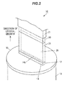
- FIG.2 is a perspective view showing a state during growth of a ⁇ -Ga 2 O 3 -based single crystal.
- a surface 26 in FIG.2 is a main surface of the ⁇ -Ga 2 O 3 -based single crystal 25 which is parallel to a slit direction of the slit 14a.
- the plane orientation of the surface 26 of the ⁇ -Ga 2 O 3 -based single crystal 25 is made to coincide with the desired plane orientation of the main surface of the ⁇ -Ga 2 O 3 -based substrate.
- the plane orientation of the surface 26 is (-201).
- the grown ⁇ -Ga 2 O 3 -based single crystal 25 also can be used as a seed crystal for growing a new ⁇ -Ga 2 O 3 -based single crystal.
- the crystal growth direction shown in FIGS.1 and 2 is a direction parallel to the b-axis of the ⁇ -Ga 2 O 3 -based single crystal 25 (the b-axis direction).
- the ⁇ -Ga 2 O 3 -based single crystal 25 and the seed crystal 20 are ⁇ -Ga 2 O 3 single crystals or Ga 2 O 3 single crystals doped with an element such as Al or In, and may be, e.g., a (Ga x Al y In (1-x-y) ) 2 O 3 (0 ⁇ x ⁇ 1, 0 ⁇ y ⁇ 1, 0 ⁇ x+y ⁇ 1) single crystal which is a ⁇ -Ga 2 O 3 single crystal doped with Al and In.
- the band gap is widened by adding Al and is narrowed by adding In.
- a Sn raw material is added to a ⁇ -Ga 2 O 3 -based raw material so that a desired Sn concentration is obtained.
- SnO 2 is added to the ⁇ -Ga 2 O 3 -based raw material so that the Sn concentration is not less than 0.005 mol% and not more than 1.0 mol%. Satisfactory properties as a conductive substrate are not obtained at the concentration of less than 0.005 mol%.
- problems such as a decrease in the doping efficiency, an increase in absorption coefficient or a decrease in yield are likely to occur at the concentration of more than 1.0 mol%.
- the following is an example of conditions of growing the ⁇ -Ga 2 O 3 -based single crystal 25 in the present embodiment.
- the ⁇ -Ga 2 O 3 -based single crystal 25 is grown in, e.g., a nitrogen atmosphere.
- the seed crystal 20 having substantially the same horizontal cross-sectional size as the Ga 2 O 3 -based single crystal 25 is used.
- a shoulder broadening process for increasing a width of the Ga 2 O 3 -based single crystal 25 is not performed. Therefore, twinning which is likely to occur in the shoulder broadening process can be suppressed.
- the seed crystal 20 is larger than a seed crystal used for typical crystal growth and is susceptible to thermal shock. Therefore, a height of the seed crystal 20 from the die 14 before the contact with the Ga 2 O 3 -based melt 12 is preferably low to some extent and is, e.g., 10 mm. In addition, a descending speed of the seed crystal 20 until the contact with the Ga 2 O 3 -based melt 12 is preferably low to some extent and is, e.g., 1 mm/min.
- Standby time until pulling up the seed crystal 20 after the contact with the Ga 2 O 3 -based melt 12 is preferably long to some extent in order to further stabilize the temperature to prevent thermal shock, and is, e.g., 10 min.
- a temperature rise rate at the time of melting the raw material in the crucible 13 is preferably low to some extent in order to prevent a rapid increase in temperature around the crucible 13 and resulting thermal shock on the seed crystal 20, and the raw material is melted over, e.g., 11 hours.
- a substrate cut out from a seed crystal of the ⁇ -Ga 2 O 3 -based single crystal grown by the above-mentioned method is mirror-polished and is then subjected to X-ray diffraction measurement to evaluate crystal quality.
- the crystal quality is evaluated by evaluating variation in crystal structure of the substrate along the direction perpendicular to the b-axis.
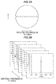
- FIG.3A is a plan view showing a substrate cut out from the ⁇ -Ga 2 O 3 -based single crystal and X-ray diffraction measurement points thereon.
- X-ray diffraction intensity is measured at measurement points shown as "x" in FIG.3A and aligned along the direction perpendicular to the b-axis while rotating the substrate about the b-axis of the ⁇ -Ga 2 O 3 -based single crystal, thereby obtaining X-ray diffraction profiles.
- the rotation angle of the substrate about the b-axis direction is defined as ⁇ [deg].
- FIG.3B is an image showing X-ray diffraction profiles which are respectively obtained from the measurement points and are aligned along the direction perpendicular to the b-axis.
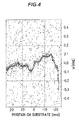
- FIG.4 is a diagram when viewing the FIG.3B from above and shows X-ray diffraction intensity distribution obtained from the measurement points.
- the horizontal axis indicates a position [mm] on the substrate in the direction perpendicular to the b-axis
- the vertical axis indicates the rotation angle ⁇ [deg] of the substrate.
- a region with high dot density represents a high X-ray diffraction intensity region and a curved line is formed by connecting the respective peak positions of the X-ray diffraction profiles obtained from the measurement points.
- positions on the substrate are located with reference to the center of the substrate as the origin.
- FIG.5 is a graph showing a curved line representing a relation between a position on the substrate and a peak position of the X-ray diffraction profile, and an approximate line thereof obtained by linear approximation using the least squares method.
- the horizontal axis indicates a position [mm] on the substrate in the direction perpendicular to the b-axis
- the vertical axis indicates the rotation angle ⁇ [deg] of the substrate.
- a difference in the rotation angle ⁇ between the peak position of the X-ray diffraction profile and the approximate line is derived for each position on the substrate, and the average value ⁇ is calculated therefrom.
- two plate-shaped ⁇ -Ga 2 O 3 -based single crystals having a (-201) plane as a main surface were grown at a Sn doping concentration of 0.05 mol%. Then, a substrate including a point 40 mm from a seed crystal as the center and a substrate including a point 90 mm from a seed crystal as the center were cut out from each of the crystals A and B. The diameter of each substrate was 50 mm.
- the width (perpendicular to the crystal growth direction) of the plate-shaped crystals A to F was 52 mm to allow a 50 mm-diameter substrate to be cut out.
- FIGS.6A and 6B are diagrams illustrating X-ray diffraction intensity distribution obtained from the measurement points on the substrates which are respectively cut out from the crystals A and B so as to include a point 40 mm from a seed crystal as the center.
- FIGS.7A and 7B are diagrams illustrating X-ray diffraction intensity distribution obtained from the measurement points on the substrates which are respectively cut out from the crystals C and D so as to include a point 40 mm from a seed crystal as the center.
- FIGS.6A, 6B , 7A and 7B correspond to FIG.4 .
- FIGS.6A, 6B , 7A and 7B show that the substrates cut out from the Sn-doped crystals A and B have smaller variation in the peak position of X-ray diffraction intensity profile in the direction perpendicular to the b-axis and thus have smaller variation in crystal structure along the direction perpendicular to the b-axis than the substrates cut out from the Si-doped crystals C and D.
- FIG.8 is a diagram showing a variation in crystal structures of the Sn-doped crystal A and B, the Si-doped crystals C and D and the non-doped crystals E and F along the direction perpendicular to the b-axis.
- the vertical axis indicates a ratio of ⁇ of each crystal to ⁇ of a seed crystal. The smaller ⁇ ratio means that variation in crystal structure along the direction perpendicular to the b-axis is closer to that of the seed crystal and quality of crystal is higher.
- the upper line is the type of crystal (the crystals A to F) from which the substrates are cut out
- the middle line is the type of the added dopant (Si, Sn or no addition)
- the lower line is a distance from the seed crystal to the center of the substrate before being cut out from the crystal.
- FIG.8 shows that the ⁇ ratio of the Sn-doped crystals A and B is smaller than the ⁇ ratio of the Si-doped crystals C and D and the crystals A and B have small variation in crystal structure along the direction perpendicular to the b-axis. It is also shown that the ⁇ ratio of the Sn-doped crystals A and B is close to the ⁇ ratio of the non-doped crystals E and F, and variation in crystal structure of the Sn-doped ⁇ -Ga 2 O 3 -based single crystal along the direction perpendicular to the b-axis is close to that of the non-doped ⁇ -Ga 2 O 3 -based single crystal.
- crystal quality of grown crystal decreases with an increase in distance from the seed crystal.
- variation in crystal structure along the direction perpendicular to the b-axis is smaller in a region of the Sn-doped crystals A and B at a distance of 90 mm from the seed crystal than in a region of the Si-doped crystals C and D at a distance of 40 mm from the seed crystal.
- Variation in crystal structure along the b-axis direction was also evaluated using the same evaluation method. As a result, variation in crystal structure along the b-axis direction was hardly observed both in the Sn-doped ⁇ -Ga 2 O 3 -based single crystals and the Si-doped ⁇ -Ga 2 O 3 -based single crystals.
- a high-quality ⁇ -Ga 2 O 3 -based single crystal having small variation in crystal structure can be grown in the b-axis direction.
- a 50 mm-diameter conductive substrate with excellent crystal quality can be obtained from a region centered at a point 40 mm from a seed crystal.
- a method for growing a ⁇ -Ga 2 O 3 -based single crystal which allows a high-quality ⁇ -Ga 2 O 3 -based single crystal having small variation in crystal structure to grow in the b-axis direction, is provided.
Landscapes
- Chemical & Material Sciences (AREA)
- Engineering & Computer Science (AREA)
- Crystallography & Structural Chemistry (AREA)
- Materials Engineering (AREA)
- Metallurgy (AREA)
- Organic Chemistry (AREA)
- Inorganic Chemistry (AREA)
- Crystals, And After-Treatments Of Crystals (AREA)
Applications Claiming Priority (2)
| Application Number | Priority Date | Filing Date | Title |
|---|---|---|---|
| JP2013078575A JP5788925B2 (ja) | 2013-04-04 | 2013-04-04 | β−Ga2O3系単結晶の成長方法 |
| PCT/JP2014/059572 WO2014163056A1 (ja) | 2013-04-04 | 2014-03-31 | β-Ga2O3系単結晶の成長方法 |
Publications (3)
| Publication Number | Publication Date |
|---|---|
| EP2990509A1 true EP2990509A1 (de) | 2016-03-02 |
| EP2990509A4 EP2990509A4 (de) | 2017-01-18 |
| EP2990509B1 EP2990509B1 (de) | 2019-12-18 |
Family
ID=51658352
Family Applications (1)
| Application Number | Title | Priority Date | Filing Date |
|---|---|---|---|
| EP14779805.2A Active EP2990509B1 (de) | 2013-04-04 | 2014-03-31 | Verfahren zur züchtung eines beta-ga2o3-basierten einkristalls |
Country Status (6)
| Country | Link |
|---|---|
| US (1) | US10526721B2 (de) |
| EP (1) | EP2990509B1 (de) |
| JP (1) | JP5788925B2 (de) |
| CN (1) | CN105102694A (de) |
| TW (1) | TWI634241B (de) |
| WO (1) | WO2014163056A1 (de) |
Families Citing this family (8)
| Publication number | Priority date | Publication date | Assignee | Title |
|---|---|---|---|---|
| JP5865867B2 (ja) * | 2013-05-13 | 2016-02-17 | 株式会社タムラ製作所 | β−Ga2O3系単結晶の育成方法、並びにβ−Ga2O3系単結晶基板の製造方法 |
| CN107541776A (zh) * | 2017-08-14 | 2018-01-05 | 同济大学 | 一种大尺寸氧化镓单晶的生长设备及方法 |
| JP7222669B2 (ja) * | 2018-11-16 | 2023-02-15 | 株式会社タムラ製作所 | 単結晶育成方法、種結晶、及び単結晶 |
| JP7436978B2 (ja) * | 2019-10-28 | 2024-02-22 | Agc株式会社 | 単結晶インゴット、結晶育成用ダイ、及び単結晶の製造方法 |
| JP2022147882A (ja) * | 2021-03-24 | 2022-10-06 | アダマンド並木精密宝石株式会社 | Ga2O3系単結晶基板と、Ga2O3系単結晶基板の製造方法 |
| KR102660564B1 (ko) * | 2021-12-29 | 2024-04-25 | 한국세라믹기술원 | Efg용 잉곳 성장장치 |
| WO2024078704A1 (en) | 2022-10-11 | 2024-04-18 | Forschungsverbund Berlin E.V. | MELT-GROWN BULK ß-(AlxGa1-x)2O3 SINGLE CRYSTALS AND METHOD FOR PRODUCING BULK ß-(AlxGA1-x)2O3 SINGLE CRYSTALS |
| KR102731513B1 (ko) * | 2022-11-14 | 2024-11-18 | 한국세라믹기술원 | 산화갈륨 단결정 성장용 분말 및 이의 제조방법 |
Family Cites Families (12)
| Publication number | Priority date | Publication date | Assignee | Title |
|---|---|---|---|---|
| JP4083396B2 (ja) | 2000-07-10 | 2008-04-30 | 独立行政法人科学技術振興機構 | 紫外透明導電膜とその製造方法 |
| JP3679097B2 (ja) * | 2002-05-31 | 2005-08-03 | 株式会社光波 | 発光素子 |
| KR100787272B1 (ko) * | 2003-02-24 | 2007-12-20 | 각코호진 와세다다이가쿠 | Ga2O3계 발광 소자 및 그 제조 방법 |
| JP4630986B2 (ja) * | 2003-02-24 | 2011-02-09 | 学校法人早稲田大学 | β−Ga2O3系単結晶成長方法 |
| JP2005235961A (ja) * | 2004-02-18 | 2005-09-02 | Univ Waseda | Ga2O3系単結晶の導電率制御方法 |
| JP2006273684A (ja) * | 2005-03-30 | 2006-10-12 | Koha Co Ltd | Iii族酸化物系単結晶の製造方法 |
| JP4611103B2 (ja) * | 2005-05-09 | 2011-01-12 | 株式会社光波 | β−Ga2O3結晶の製造方法 |
| JP2008037725A (ja) * | 2006-08-10 | 2008-02-21 | Nippon Light Metal Co Ltd | 酸化ガリウム単結晶の製造方法 |
| JP2008156141A (ja) * | 2006-12-21 | 2008-07-10 | Koha Co Ltd | 半導体基板及びその製造方法 |
| JP5786179B2 (ja) | 2010-03-12 | 2015-09-30 | 並木精密宝石株式会社 | 酸化ガリウム単結晶及びその製造方法 |
| US9461124B2 (en) | 2011-09-08 | 2016-10-04 | Tamura Corporation | Ga2O3 semiconductor element |
| JP5491483B2 (ja) * | 2011-11-15 | 2014-05-14 | 株式会社タムラ製作所 | β−Ga2O3系単結晶の成長方法 |
-
2013
- 2013-04-04 JP JP2013078575A patent/JP5788925B2/ja active Active
-
2014
- 2014-03-31 EP EP14779805.2A patent/EP2990509B1/de active Active
- 2014-03-31 US US14/782,039 patent/US10526721B2/en active Active
- 2014-03-31 CN CN201480020148.XA patent/CN105102694A/zh active Pending
- 2014-03-31 WO PCT/JP2014/059572 patent/WO2014163056A1/ja not_active Ceased
- 2014-04-03 TW TW103112566A patent/TWI634241B/zh active
Non-Patent Citations (1)
| Title |
|---|
| See references of WO2014163056A1 * |
Also Published As
| Publication number | Publication date |
|---|---|
| US20160032485A1 (en) | 2016-02-04 |
| JP2014201480A (ja) | 2014-10-27 |
| EP2990509B1 (de) | 2019-12-18 |
| CN105102694A (zh) | 2015-11-25 |
| WO2014163056A1 (ja) | 2014-10-09 |
| JP5788925B2 (ja) | 2015-10-07 |
| TW201443301A (zh) | 2014-11-16 |
| TWI634241B (zh) | 2018-09-01 |
| EP2990509A4 (de) | 2017-01-18 |
| US10526721B2 (en) | 2020-01-07 |
Similar Documents
| Publication | Publication Date | Title |
|---|---|---|
| US10526721B2 (en) | Method for growing β-GA2O3-based single crystal | |
| EP2801645B1 (de) | Verfahren zur züchtung von beta-ga2o3-basierten einkristallen | |
| JP5233070B2 (ja) | 燐化インジウム基板および燐化インジウム単結晶とその製造方法 | |
| JP5786179B2 (ja) | 酸化ガリウム単結晶及びその製造方法 | |
| US8328935B2 (en) | Method of manufacturing polycrystalline silicon rod | |
| US10633761B2 (en) | GA2O3-based single crystal substrate, and production method therefor | |
| EP2767621B1 (de) | Verfahren zur herstellung von b-ga2o3-substrat und verfahren zur herstellung einer kristalllaminatstruktur | |
| EP2933359B1 (de) | Verfahren zur züchtung eines beta-ga2o3-basierten einkristalls | |
| CN114561701B (zh) | 一种铸造法生长氧化镓单晶的方法及包含氧化镓单晶的半导体器件 | |
| JP2014205618A (ja) | β−Ga2O3系単結晶及び基板 | |
| JP5172881B2 (ja) | 化合物半導体単結晶の製造装置及びその製造方法 | |
| JP5777756B2 (ja) | β−Ga2O3系単結晶基板 | |
| JP7536916B2 (ja) | 単結晶 | |
| JP4193681B2 (ja) | リン化ガリウム単結晶製造装置 | |
| JP2005162500A (ja) | InP単結晶の製造方法 |
Legal Events
| Date | Code | Title | Description |
|---|---|---|---|
| PUAI | Public reference made under article 153(3) epc to a published international application that has entered the european phase |
Free format text: ORIGINAL CODE: 0009012 |
|
| 17P | Request for examination filed |
Effective date: 20151104 |
|
| AK | Designated contracting states |
Kind code of ref document: A1 Designated state(s): AL AT BE BG CH CY CZ DE DK EE ES FI FR GB GR HR HU IE IS IT LI LT LU LV MC MK MT NL NO PL PT RO RS SE SI SK SM TR |
|
| AX | Request for extension of the european patent |
Extension state: BA ME |
|
| DAX | Request for extension of the european patent (deleted) | ||
| A4 | Supplementary search report drawn up and despatched |
Effective date: 20161221 |
|
| RIC1 | Information provided on ipc code assigned before grant |
Ipc: C30B 29/16 20060101AFI20161215BHEP Ipc: C30B 15/34 20060101ALI20161215BHEP |
|
| GRAP | Despatch of communication of intention to grant a patent |
Free format text: ORIGINAL CODE: EPIDOSNIGR1 |
|
| STAA | Information on the status of an ep patent application or granted ep patent |
Free format text: STATUS: GRANT OF PATENT IS INTENDED |
|
| INTG | Intention to grant announced |
Effective date: 20190705 |
|
| GRAS | Grant fee paid |
Free format text: ORIGINAL CODE: EPIDOSNIGR3 |
|
| GRAA | (expected) grant |
Free format text: ORIGINAL CODE: 0009210 |
|
| STAA | Information on the status of an ep patent application or granted ep patent |
Free format text: STATUS: THE PATENT HAS BEEN GRANTED |
|
| AK | Designated contracting states |
Kind code of ref document: B1 Designated state(s): AL AT BE BG CH CY CZ DE DK EE ES FI FR GB GR HR HU IE IS IT LI LT LU LV MC MK MT NL NO PL PT RO RS SE SI SK SM TR |
|
| REG | Reference to a national code |
Ref country code: CH Ref legal event code: EP |
|
| REG | Reference to a national code |
Ref country code: DE Ref legal event code: R096 Ref document number: 602014058625 Country of ref document: DE |
|
| REG | Reference to a national code |
Ref country code: IE Ref legal event code: FG4D |
|
| REG | Reference to a national code |
Ref country code: AT Ref legal event code: REF Ref document number: 1214695 Country of ref document: AT Kind code of ref document: T Effective date: 20200115 |
|
| REG | Reference to a national code |
Ref country code: NL Ref legal event code: MP Effective date: 20191218 |
|
| PG25 | Lapsed in a contracting state [announced via postgrant information from national office to epo] |
Ref country code: BG Free format text: LAPSE BECAUSE OF FAILURE TO SUBMIT A TRANSLATION OF THE DESCRIPTION OR TO PAY THE FEE WITHIN THE PRESCRIBED TIME-LIMIT Effective date: 20200318 Ref country code: FI Free format text: LAPSE BECAUSE OF FAILURE TO SUBMIT A TRANSLATION OF THE DESCRIPTION OR TO PAY THE FEE WITHIN THE PRESCRIBED TIME-LIMIT Effective date: 20191218 Ref country code: SE Free format text: LAPSE BECAUSE OF FAILURE TO SUBMIT A TRANSLATION OF THE DESCRIPTION OR TO PAY THE FEE WITHIN THE PRESCRIBED TIME-LIMIT Effective date: 20191218 Ref country code: LV Free format text: LAPSE BECAUSE OF FAILURE TO SUBMIT A TRANSLATION OF THE DESCRIPTION OR TO PAY THE FEE WITHIN THE PRESCRIBED TIME-LIMIT Effective date: 20191218 Ref country code: NO Free format text: LAPSE BECAUSE OF FAILURE TO SUBMIT A TRANSLATION OF THE DESCRIPTION OR TO PAY THE FEE WITHIN THE PRESCRIBED TIME-LIMIT Effective date: 20200318 Ref country code: LT Free format text: LAPSE BECAUSE OF FAILURE TO SUBMIT A TRANSLATION OF THE DESCRIPTION OR TO PAY THE FEE WITHIN THE PRESCRIBED TIME-LIMIT Effective date: 20191218 Ref country code: GR Free format text: LAPSE BECAUSE OF FAILURE TO SUBMIT A TRANSLATION OF THE DESCRIPTION OR TO PAY THE FEE WITHIN THE PRESCRIBED TIME-LIMIT Effective date: 20200319 |
|
| REG | Reference to a national code |
Ref country code: LT Ref legal event code: MG4D |
|
| PG25 | Lapsed in a contracting state [announced via postgrant information from national office to epo] |
Ref country code: HR Free format text: LAPSE BECAUSE OF FAILURE TO SUBMIT A TRANSLATION OF THE DESCRIPTION OR TO PAY THE FEE WITHIN THE PRESCRIBED TIME-LIMIT Effective date: 20191218 Ref country code: RS Free format text: LAPSE BECAUSE OF FAILURE TO SUBMIT A TRANSLATION OF THE DESCRIPTION OR TO PAY THE FEE WITHIN THE PRESCRIBED TIME-LIMIT Effective date: 20191218 |
|
| PG25 | Lapsed in a contracting state [announced via postgrant information from national office to epo] |
Ref country code: AL Free format text: LAPSE BECAUSE OF FAILURE TO SUBMIT A TRANSLATION OF THE DESCRIPTION OR TO PAY THE FEE WITHIN THE PRESCRIBED TIME-LIMIT Effective date: 20191218 |
|
| PG25 | Lapsed in a contracting state [announced via postgrant information from national office to epo] |
Ref country code: EE Free format text: LAPSE BECAUSE OF FAILURE TO SUBMIT A TRANSLATION OF THE DESCRIPTION OR TO PAY THE FEE WITHIN THE PRESCRIBED TIME-LIMIT Effective date: 20191218 Ref country code: NL Free format text: LAPSE BECAUSE OF FAILURE TO SUBMIT A TRANSLATION OF THE DESCRIPTION OR TO PAY THE FEE WITHIN THE PRESCRIBED TIME-LIMIT Effective date: 20191218 Ref country code: RO Free format text: LAPSE BECAUSE OF FAILURE TO SUBMIT A TRANSLATION OF THE DESCRIPTION OR TO PAY THE FEE WITHIN THE PRESCRIBED TIME-LIMIT Effective date: 20191218 Ref country code: CZ Free format text: LAPSE BECAUSE OF FAILURE TO SUBMIT A TRANSLATION OF THE DESCRIPTION OR TO PAY THE FEE WITHIN THE PRESCRIBED TIME-LIMIT Effective date: 20191218 Ref country code: PT Free format text: LAPSE BECAUSE OF FAILURE TO SUBMIT A TRANSLATION OF THE DESCRIPTION OR TO PAY THE FEE WITHIN THE PRESCRIBED TIME-LIMIT Effective date: 20200513 |
|
| PG25 | Lapsed in a contracting state [announced via postgrant information from national office to epo] |
Ref country code: SM Free format text: LAPSE BECAUSE OF FAILURE TO SUBMIT A TRANSLATION OF THE DESCRIPTION OR TO PAY THE FEE WITHIN THE PRESCRIBED TIME-LIMIT Effective date: 20191218 Ref country code: SK Free format text: LAPSE BECAUSE OF FAILURE TO SUBMIT A TRANSLATION OF THE DESCRIPTION OR TO PAY THE FEE WITHIN THE PRESCRIBED TIME-LIMIT Effective date: 20191218 Ref country code: IS Free format text: LAPSE BECAUSE OF FAILURE TO SUBMIT A TRANSLATION OF THE DESCRIPTION OR TO PAY THE FEE WITHIN THE PRESCRIBED TIME-LIMIT Effective date: 20200418 |
|
| REG | Reference to a national code |
Ref country code: DE Ref legal event code: R097 Ref document number: 602014058625 Country of ref document: DE |
|
| REG | Reference to a national code |
Ref country code: AT Ref legal event code: MK05 Ref document number: 1214695 Country of ref document: AT Kind code of ref document: T Effective date: 20191218 |
|
| PLBE | No opposition filed within time limit |
Free format text: ORIGINAL CODE: 0009261 |
|
| STAA | Information on the status of an ep patent application or granted ep patent |
Free format text: STATUS: NO OPPOSITION FILED WITHIN TIME LIMIT |
|
| PG25 | Lapsed in a contracting state [announced via postgrant information from national office to epo] |
Ref country code: DK Free format text: LAPSE BECAUSE OF FAILURE TO SUBMIT A TRANSLATION OF THE DESCRIPTION OR TO PAY THE FEE WITHIN THE PRESCRIBED TIME-LIMIT Effective date: 20191218 Ref country code: ES Free format text: LAPSE BECAUSE OF FAILURE TO SUBMIT A TRANSLATION OF THE DESCRIPTION OR TO PAY THE FEE WITHIN THE PRESCRIBED TIME-LIMIT Effective date: 20191218 Ref country code: MC Free format text: LAPSE BECAUSE OF FAILURE TO SUBMIT A TRANSLATION OF THE DESCRIPTION OR TO PAY THE FEE WITHIN THE PRESCRIBED TIME-LIMIT Effective date: 20191218 |
|
| REG | Reference to a national code |
Ref country code: CH Ref legal event code: PL |
|
| 26N | No opposition filed |
Effective date: 20200921 |
|
| PG25 | Lapsed in a contracting state [announced via postgrant information from national office to epo] |
Ref country code: SI Free format text: LAPSE BECAUSE OF FAILURE TO SUBMIT A TRANSLATION OF THE DESCRIPTION OR TO PAY THE FEE WITHIN THE PRESCRIBED TIME-LIMIT Effective date: 20191218 Ref country code: AT Free format text: LAPSE BECAUSE OF FAILURE TO SUBMIT A TRANSLATION OF THE DESCRIPTION OR TO PAY THE FEE WITHIN THE PRESCRIBED TIME-LIMIT Effective date: 20191218 |
|
| PG25 | Lapsed in a contracting state [announced via postgrant information from national office to epo] |
Ref country code: LU Free format text: LAPSE BECAUSE OF NON-PAYMENT OF DUE FEES Effective date: 20200331 |
|
| PG25 | Lapsed in a contracting state [announced via postgrant information from national office to epo] |
Ref country code: LI Free format text: LAPSE BECAUSE OF NON-PAYMENT OF DUE FEES Effective date: 20200331 Ref country code: IE Free format text: LAPSE BECAUSE OF NON-PAYMENT OF DUE FEES Effective date: 20200331 Ref country code: IT Free format text: LAPSE BECAUSE OF FAILURE TO SUBMIT A TRANSLATION OF THE DESCRIPTION OR TO PAY THE FEE WITHIN THE PRESCRIBED TIME-LIMIT Effective date: 20191218 Ref country code: CH Free format text: LAPSE BECAUSE OF NON-PAYMENT OF DUE FEES Effective date: 20200331 |
|
| PG25 | Lapsed in a contracting state [announced via postgrant information from national office to epo] |
Ref country code: PL Free format text: LAPSE BECAUSE OF FAILURE TO SUBMIT A TRANSLATION OF THE DESCRIPTION OR TO PAY THE FEE WITHIN THE PRESCRIBED TIME-LIMIT Effective date: 20191218 |
|
| GBPC | Gb: european patent ceased through non-payment of renewal fee |
Effective date: 20200331 |
|
| PG25 | Lapsed in a contracting state [announced via postgrant information from national office to epo] |
Ref country code: GB Free format text: LAPSE BECAUSE OF NON-PAYMENT OF DUE FEES Effective date: 20200331 |
|
| REG | Reference to a national code |
Ref country code: DE Ref legal event code: R081 Ref document number: 602014058625 Country of ref document: DE Owner name: TAMURA CORP., JP Free format text: FORMER OWNERS: KOHA CO., LTD., TOKYO, JP; TAMURA CORP., TOKYO, JP |
|
| PG25 | Lapsed in a contracting state [announced via postgrant information from national office to epo] |
Ref country code: TR Free format text: LAPSE BECAUSE OF FAILURE TO SUBMIT A TRANSLATION OF THE DESCRIPTION OR TO PAY THE FEE WITHIN THE PRESCRIBED TIME-LIMIT Effective date: 20191218 Ref country code: MT Free format text: LAPSE BECAUSE OF FAILURE TO SUBMIT A TRANSLATION OF THE DESCRIPTION OR TO PAY THE FEE WITHIN THE PRESCRIBED TIME-LIMIT Effective date: 20191218 Ref country code: CY Free format text: LAPSE BECAUSE OF FAILURE TO SUBMIT A TRANSLATION OF THE DESCRIPTION OR TO PAY THE FEE WITHIN THE PRESCRIBED TIME-LIMIT Effective date: 20191218 |
|
| REG | Reference to a national code |
Ref country code: BE Ref legal event code: PD Owner name: TAMURA CORPORATION; JP Free format text: DETAILS ASSIGNMENT: CHANGE OF OWNER(S), ASSIGNMENT; FORMER OWNER NAME: KOHA CO., LTD. Effective date: 20220429 |
|
| PG25 | Lapsed in a contracting state [announced via postgrant information from national office to epo] |
Ref country code: MK Free format text: LAPSE BECAUSE OF FAILURE TO SUBMIT A TRANSLATION OF THE DESCRIPTION OR TO PAY THE FEE WITHIN THE PRESCRIBED TIME-LIMIT Effective date: 20191218 |
|
| REG | Reference to a national code |
Ref country code: DE Ref legal event code: R082 Ref document number: 602014058625 Country of ref document: DE Representative=s name: DENNEMEYER & ASSOCIATES RECHTSANWALTSGESELLSCH, DE |
|
| PGFP | Annual fee paid to national office [announced via postgrant information from national office to epo] |
Ref country code: DE Payment date: 20260319 Year of fee payment: 13 |
|
| PGFP | Annual fee paid to national office [announced via postgrant information from national office to epo] |
Ref country code: BE Payment date: 20260319 Year of fee payment: 13 |
|
| PGFP | Annual fee paid to national office [announced via postgrant information from national office to epo] |
Ref country code: FR Payment date: 20260320 Year of fee payment: 13 |