EP3000664B1 - Control apparatus, connector, and laminated capacitor for connector - Google Patents
Control apparatus, connector, and laminated capacitor for connector Download PDFInfo
- Publication number
- EP3000664B1 EP3000664B1 EP14801888.0A EP14801888A EP3000664B1 EP 3000664 B1 EP3000664 B1 EP 3000664B1 EP 14801888 A EP14801888 A EP 14801888A EP 3000664 B1 EP3000664 B1 EP 3000664B1
- Authority
- EP
- European Patent Office
- Prior art keywords
- ground
- terminal
- circuit pattern
- connector
- pattern
- Prior art date
- Legal status (The legal status is an assumption and is not a legal conclusion. Google has not performed a legal analysis and makes no representation as to the accuracy of the status listed.)
- Active
Links
Images





Classifications
-
- H—ELECTRICITY
- H01—ELECTRIC ELEMENTS
- H01R—ELECTRICALLY-CONDUCTIVE CONNECTIONS; STRUCTURAL ASSOCIATIONS OF A PLURALITY OF MUTUALLY-INSULATED ELECTRICAL CONNECTING ELEMENTS; COUPLING DEVICES; CURRENT COLLECTORS
- H01R13/00—Details of coupling devices of the kinds covered by groups H01R12/70 or H01R24/00 - H01R33/00
- H01R13/66—Structural association with built-in electrical component
- H01R13/6608—Structural association with built-in electrical component with built-in single component
- H01R13/6625—Structural association with built-in electrical component with built-in single component with capacitive component
-
- H—ELECTRICITY
- H01—ELECTRIC ELEMENTS
- H01G—CAPACITORS; CAPACITORS, RECTIFIERS, DETECTORS, SWITCHING DEVICES, LIGHT-SENSITIVE OR TEMPERATURE-SENSITIVE DEVICES OF THE ELECTROLYTIC TYPE
- H01G4/00—Fixed capacitors; Processes of their manufacture
- H01G4/30—Stacked capacitors
-
- H—ELECTRICITY
- H01—ELECTRIC ELEMENTS
- H01G—CAPACITORS; CAPACITORS, RECTIFIERS, DETECTORS, SWITCHING DEVICES, LIGHT-SENSITIVE OR TEMPERATURE-SENSITIVE DEVICES OF THE ELECTROLYTIC TYPE
- H01G2/00—Details of capacitors not covered by a single one of groups H01G4/00-H01G11/00
- H01G2/02—Mountings
- H01G2/06—Mountings specially adapted for mounting on a printed-circuit support
-
- H—ELECTRICITY
- H01—ELECTRIC ELEMENTS
- H01G—CAPACITORS; CAPACITORS, RECTIFIERS, DETECTORS, SWITCHING DEVICES, LIGHT-SENSITIVE OR TEMPERATURE-SENSITIVE DEVICES OF THE ELECTROLYTIC TYPE
- H01G4/00—Fixed capacitors; Processes of their manufacture
- H01G4/002—Details
- H01G4/005—Electrodes
- H01G4/012—Form of non-self-supporting electrodes
-
- H—ELECTRICITY
- H01—ELECTRIC ELEMENTS
- H01G—CAPACITORS; CAPACITORS, RECTIFIERS, DETECTORS, SWITCHING DEVICES, LIGHT-SENSITIVE OR TEMPERATURE-SENSITIVE DEVICES OF THE ELECTROLYTIC TYPE
- H01G4/00—Fixed capacitors; Processes of their manufacture
- H01G4/002—Details
- H01G4/018—Dielectrics
- H01G4/06—Solid dielectrics
- H01G4/08—Inorganic dielectrics
- H01G4/12—Ceramic dielectrics
-
- H—ELECTRICITY
- H01—ELECTRIC ELEMENTS
- H01G—CAPACITORS; CAPACITORS, RECTIFIERS, DETECTORS, SWITCHING DEVICES, LIGHT-SENSITIVE OR TEMPERATURE-SENSITIVE DEVICES OF THE ELECTROLYTIC TYPE
- H01G4/00—Fixed capacitors; Processes of their manufacture
- H01G4/002—Details
- H01G4/228—Terminals
-
- H—ELECTRICITY
- H01—ELECTRIC ELEMENTS
- H01G—CAPACITORS; CAPACITORS, RECTIFIERS, DETECTORS, SWITCHING DEVICES, LIGHT-SENSITIVE OR TEMPERATURE-SENSITIVE DEVICES OF THE ELECTROLYTIC TYPE
- H01G4/00—Fixed capacitors; Processes of their manufacture
- H01G4/002—Details
- H01G4/228—Terminals
- H01G4/232—Terminals electrically connecting two or more layers of a stacked or rolled capacitor
-
- H—ELECTRICITY
- H01—ELECTRIC ELEMENTS
- H01G—CAPACITORS; CAPACITORS, RECTIFIERS, DETECTORS, SWITCHING DEVICES, LIGHT-SENSITIVE OR TEMPERATURE-SENSITIVE DEVICES OF THE ELECTROLYTIC TYPE
- H01G4/00—Fixed capacitors; Processes of their manufacture
- H01G4/40—Structural combinations of fixed capacitors with other electric elements, the structure mainly consisting of a capacitor, e.g. RC combinations
-
- H—ELECTRICITY
- H01—ELECTRIC ELEMENTS
- H01R—ELECTRICALLY-CONDUCTIVE CONNECTIONS; STRUCTURAL ASSOCIATIONS OF A PLURALITY OF MUTUALLY-INSULATED ELECTRICAL CONNECTING ELEMENTS; COUPLING DEVICES; CURRENT COLLECTORS
- H01R13/00—Details of coupling devices of the kinds covered by groups H01R12/70 or H01R24/00 - H01R33/00
- H01R13/646—Details of coupling devices of the kinds covered by groups H01R12/70 or H01R24/00 - H01R33/00 specially adapted for high-frequency, e.g. structures providing an impedance match or phase match
- H01R13/6461—Means for preventing cross-talk
- H01R13/6464—Means for preventing cross-talk by adding capacitive elements
- H01R13/6466—Means for preventing cross-talk by adding capacitive elements on substrates, e.g. printed circuit boards [PCB]
-
- H—ELECTRICITY
- H05—ELECTRIC TECHNIQUES NOT OTHERWISE PROVIDED FOR
- H05K—PRINTED CIRCUITS; CASINGS OR CONSTRUCTIONAL DETAILS OF ELECTRIC APPARATUS; MANUFACTURE OF ASSEMBLAGES OF ELECTRICAL COMPONENTS
- H05K1/00—Printed circuits
- H05K1/18—Printed circuits structurally associated with non-printed electric components
-
- H—ELECTRICITY
- H01—ELECTRIC ELEMENTS
- H01G—CAPACITORS; CAPACITORS, RECTIFIERS, DETECTORS, SWITCHING DEVICES, LIGHT-SENSITIVE OR TEMPERATURE-SENSITIVE DEVICES OF THE ELECTROLYTIC TYPE
- H01G4/00—Fixed capacitors; Processes of their manufacture
- H01G4/002—Details
- H01G4/228—Terminals
- H01G4/236—Terminals leading through the housing, i.e. lead-through
Definitions
- the present invention relates to a control apparatus, a connector, and a laminated capacitor for connector, and relates to, for example, an in-vehicle control apparatus for in-vehicle equipment installed in a vehicle, a connector for the control apparatus, and a laminated capacitor for the connector.
- control apparatuses electronic control units or ECUs
- ECUs electronic control units
- a recent vehicle is equipped with, for example, air-conditioning equipment and audio equipment, information equipment such as a navigation system, safety equipment such as a camera and a sensor for obtaining information outside the car, motor-driven equipment such as a power window, a power seat, and a power steering, and other equipment; thus, in order to precisely control these various pieces of in-vehicle equipment, even more control apparatuses are embedded.
- each control apparatus is equipped with even more input/output terminals to improve function of each control apparatus; thus, it is becoming difficult to appropriately dispose such highly functionalized control apparatuses in a restricted space in the vehicle.
- PTLs 1 to 3 disclose a technology which makes the whole of a control apparatus small and light by embedding capacitors in a connector, where the capacitors block or reduce noise and static electricity which are caused by operations of a motor and an injector (fuel injection valve) installed in the vehicle or caused by energization of wires.
- a capacitor is electrically connected between a connection part at which a power source side capacitor is connected to a power source side bus bar and a connection part at which an earth side capacitor is connected to an earth side bus bar; and in a connector housing, a positioning member is provided to guide the capacitor to be disposed between the connection parts.
- a capacitor is attached to a pair of power source connection terminals of the connector, and the pair of power source connection terminals are electrically connected through the capacitor.
- a connector is combined with a feedthrough capacitor formed of a laminated component, wherein the feed through capacitor is made of conductor and dielectric material laminated in a block shape, near the conductor there are provided through holes or notches through each of which each of a plurality of metal terminal of the connector passes, and the feedthrough capacitor has on the outer surface a ground terminal connected to the conductor.
- PTL4 discloses a filter capacitor for filter feedthrough assemblies which maintains its shape and structure dimensions after undergoing numerous sintering steps.
- the capacitor built in the connector is formed of a main body having an approximate cuboid shape or formed of a pillar whose cross section is an ellipse; therefore, there is a problem that if the number of the input/output terminals becomes large due to higher functionality of the control apparatus as described above, the whole of the control apparatus becomes large.
- the feedthrough capacitor is formed in the process: after dielectric material such as silicon dioxide and conductor for electrode made of silver or the like are serially laminated by a printing method or a sheet method and are sintered or after a laminated body having a block shape is formed by a sputtering method or an evaporation method, the terminal connected to the conductor is glazed on the outer surface of the block; and then, the dielectric material and the conductor for electrode are laminated in the vertical direction; thus, there is a problem that it is difficult to precisely adjust the capacitor capacitances on the terminals.
- the present invention is made in view of the above problem, and an object of the invention is to provide a control apparatus, a connector, and a laminated capacitor for connector which are small and light and in which the capacitor capacitances on the terminals can be easily adjusted.
- a control apparatus includes: a substrate on which an electronic component for controlling an external device is mounted; a connector which electrically connects the substrate to the external device or external wires, and the connector includes: a plurality of connection terminals which connect the substrate to the external device or the external wires; and a laminated capacitor in which a terminal dielectric sheet on which a terminal circuit pattern is printed and a ground dielectric sheet on which a ground circuit pattern is printed are alternately laminated into one body, and the terminal circuit pattern includes terminal connecting patterns electrically connected to the plurality of connection terminals; and terminal-side electrode patterns connected to the terminal connecting patterns, and the ground circuit pattern includes: ground-side electrode patterns disposed to face the terminal-side electrode patterns; and a ground pattern connected to the ground-side electrode patterns.
- a connector according to the present invention is a connecter which electrically connects a substrate, on which an electronic component for controlling an external device is mounted, to the external device or external wires, the connector including: a plurality of connection terminals which connect the substrate to the external device or the external wires; and a laminated capacitor in which a terminal dielectric sheet on which a terminal circuit pattern is printed and a ground dielectric sheet on which a ground circuit pattern is printed are alternately laminated into one body, wherein the terminal circuit pattern includes: terminal connecting patterns electrically connected to the plurality of connection terminals; and terminal-side electrode patterns connected to the terminal connecting patterns, and the ground circuit pattern includes: ground-side electrode patterns disposed to face the terminal-side electrode patterns; and a ground pattern connected to the ground-side electrode patterns.
- a laminated capacitor according to the present invention is a laminated capacitor for a connector which electrically connects a substrate, on which an electronic component for controlling an external device is mounted, to the external device or external wires, the laminated capacitor including: a terminal dielectric sheet and a ground dielectric sheet which are alternately laminated into one body, wherein on the terminal dielectric sheet, a terminal circuit pattern having terminal connecting patterns electrically connected to a plurality of connection terminals which connect the substrate to the external device or the external wires and terminal-side electrode patterns connected to the terminal connecting patterns is printed, and on the ground dielectric sheet, a ground circuit pattern having ground-side electrode patterns disposed to face the terminal-side electrode patterns and a ground pattern connected to the ground-side electrode patterns is printed.
- the laminated capacitor constituting the control apparatus, the connector, and the laminated capacitor for connector is made of a terminal dielectric sheet on which a terminal circuit pattern is printed and a ground dielectric sheet on which a ground circuit pattern is printed are alternately laminated into one body; therefore, the control apparatus, the connector, and the laminated capacitor for connector can be small and light even in a case that the number of the input/output terminals becomes large due to, for example, higher functionality of the control apparatus; and in addition, when the electrode patterns on a terminal side and a ground side of the circuit patterns for the terminals and the ground are modified at the time of manufacturing the terminal dielectric sheet and the ground dielectric sheet, the capacitor capacitances on the connection terminals can be easily adjusted.
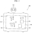
- Fig. 1 shows a basic configuration of a first embodiment of the control apparatus according to the present invention.
- Fig. 2 shows a lower surface of the control apparatus shown in Fig. 1 in an exploded state.
- Fig. 3 shows the connector shown in Fig. 2 in an exploded state
- Fig. 4 shows a vertical sectional view of the connector shown in Fig. 3 in an exploded state
- Fig. 5 shows A part in Fig. 4 in an enlarged state.
- the control apparatus (electronic control unit or ECU) 100 is mainly equipped with a main body case 101 and a printed circuit board (substrate) 105 fixedly disposed on the main body case 101 with fixing members 102 such as screws.
- the printed circuit board 105 On the printed circuit board 105, electronic components such as an IC 103, a capacitor 104, and the like are mounted at appropriate positions by soldering or the like, where the IC 103 controls, for example, an external device such as in-vehicle equipment installed in a vehicle.
- the printed circuit board 105 is formed of, for example, insulating resin or the like such as glass epoxy resin; on the surface of the printed circuit board 105, an appropriate wiring circuit pattern (not shown) is formed; and the above electronic components and the wiring circuit pattern constitute a control circuit which controls the external device.
- an approximately rectangular through-hole 106 is formed as shown Fig. 2 , a connector 110 is fit in the through-hole 106, and the printed circuit board 105 is electrically connected to the external device and external wires through the connector 110.
- the connector 110 mainly includes a plurality of connection terminals 111 for connecting the printed circuit board 105 to the external device and the external wires, a connector housing 112 for housing and protecting the plurality of connection terminals 111, a laminated ceramic capacitor (laminated capacitor) 113 for blocking or reducing noise and static electricity which are caused by operations of actuators such as a motor and an injector (fuel injection valve) installed in the vehicle or caused by energization of the wires.
- actuators such as a motor and an injector (fuel injection valve) installed in the vehicle or caused by energization of the wires.
- connection terminals 111 have a rod shape and include, for example, 100 pieces or more of input/output pins 111a and a ground pin 111b as described later (see Fig. 6 ).
- the connector housing 112 mainly has: a cylindrical body 114 having an approximately rectangular cross-section and a shape complementary to the through-hole 106 in the main body case 101 and surrounding the plurality of connection terminals 111; and a bottom plate 115 closing an end part of the cylindrical body 114 on the printed circuit board 105 side.
- a projection portion 116 which defines a position of the connector housing 112 with respect to the main body case 101 when the connector housing 112 is fit into the through-hole 106 in the main body case 101.
- the bottom plate 115 there is formed as shown in Fig. 4 through-holes 117 through each of which a part of the connection terminal 111 passes, and approximately at the center of the bottom plate 115 there is formed a positioning part 118 to position the laminated ceramic capacitor 113.
- a thick part 119 is formed to hold the shape of the cylindrical body 114, and in the area defined by the bottom plate 115 and the thick part 119, the laminated ceramic capacitor 113 is disposed.
- an elastic resin adhesive member (buffering member) 120 formed of silicon or the like, for example; and the laminated ceramic capacitor 113 is integrally and fixedly disposed on the connector housing 112 in a posture of being clamped by the resin adhesive member 120 and being in contact with the bottom plate 115.
- the through-holes 121 through which the connection terminals 111 pass and a positioning hole 122 through which the positioning part 118 passes, at the positions corresponding to the through-holes 117 formed in the bottom plate 115 of the connector housing 112 and the positioning part 118.
- Fig. 6 shows a part of the laminated ceramic capacitor shown in Fig. 4 in an enlarged state.
- Fig. 7A shows a terminal dielectric sheet for forming the laminated ceramic capacitor shown in Fig. 6
- Fig. 7B shows a ground dielectric sheet for the laminated ceramic capacitor.
- the laminated ceramic capacitor 113 is formed such that the terminal dielectric sheet on which a terminal circuit pattern P10a is printed and the ground dielectric sheet on which a ground circuit pattern P10b is printed are alternately laminated into one body.
- connection terminals 111 there are formed in a lamination direction the through-holes 121 through which the connection terminals 111 pass; the input/output pins 111a of the connection terminals 111 are fit, in the lamination direction, in the through-holes 121a, for the terminal, of the through-holes 121 and are electrically connected to the terminal circuit pattern P10a; and the ground pin 111b of the connection terminals 111 is fit, in the lamination direction, in the through-hole 121b, for the ground, of the through-holes 121 and is electrically connected to the ground circuit pattern P10b.
- the laminated ceramic capacitor 113 is formed such that a terminal dielectric sheet 123a and a ground dielectric sheet 123b are alternately laminated, where on the terminal dielectric sheet 123a, the terminal circuit pattern P10a formed of terminal connecting patterns P12a to be electrically connected to the input/output pins 111a of the connection terminals 111 and the terminal-side electrode patterns P11a connected to the terminal connecting patterns P12a is printed, and where on the ground dielectric sheet 123b, the ground circuit pattern P10b formed of ground-side electrode patterns P11b which are disposed to face the terminal-side electrode patterns P11a (are disposed to overlap the terminal-side electrode patterns P11a when viewed from the lamination direction) and a ground pattern P12b connected to the ground-side electrode patterns P11b is printed.
- the plurality of input/output pins 111a are fit, in the lamination direction, in through-holes 121aa (121a) each formed in each of the terminal connecting patterns P12a on the terminal circuit patterns P10a, so that the input/output pins 111a and the terminal circuit patterns P10a are electrically connected.
- the ground dielectric sheets 123b there are formed through-holes 121ab (121a) through which the input/output pins 111a pass, in the lamination direction, at the positions corresponding to the terminal connecting patterns P12a, so that the input/output pins 111a and the ground circuit pattern P10b are not electrically connected.
- the ground pin 111b is fit, in the lamination direction, in the through-hole 121bb (121b) formed in the ground pattern P12b of the ground circuit pattern P10b, in particular, in the ground part P12c of the ground pattern P12b, so that the ground pin 111b and the ground circuit pattern P10b are electrically connected.
- the terminal dielectric sheet 123a there is formed a through-hole 121ba (121b) through which the ground pin 111b passes, in the lamination direction, at the position corresponding to the ground part P12c of the ground pattern P12b, so that the ground pin 111b and the terminal circuit pattern P10a are not electrically connected.
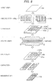
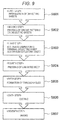
- slurry dielectric material (ceramic material) of, for example, barium titanate or the like is formed in a sheet shape, and a dielectric sheet 123 having a thickness of, for example, approximately 1 ⁇ m is prepared (S801 of Fig. 9 ).
- circuit patterns (the terminal circuit patterns P10a or the ground circuit pattern P10b) made of, for example, nickel paste are printed on the dielectric sheets 123, so that the terminal dielectric sheets 123a and the ground dielectric sheets 123b are prepared (S802 of Fig. 9 ).
- the terminal dielectric sheet 123a and the ground dielectric sheet 123b are alternately laminated (for example, 300 layers for each or total of 600 layers) in the appropriate orientation to prepare a laminated body 124 (S803 of Fig. 9 ). Note that the number of laminations of the terminal dielectric sheets 123a and the ground dielectric sheets 123b can be changed depending on the required capacitor capacitance.
- the laminated body 124 is pressed in the lamination direction by a pressing machine with a previously set pressure to prepare a laminated ceramic 125 (S804 of Fig. 9 ).
- a through-hole process by using, for example, an inter-layer contacting technique for printed circuit boards is performed on the laminated ceramic 125 to form the through-holes 121a and 121b having an appropriate size at the positions corresponding to the terminal connecting patterns P12a of the terminal circuit pattern P10a on the terminal dielectric sheet 123a and at the position corresponding to the ground part P12c of the ground pattern P12b of the ground circuit pattern P10b on the ground dielectric sheet 123b (S805 of Fig. 9 ).
- end faces of the through-holes 121a and 121b may be processed by using an appropriate end face processing technique for printed circuit boards or the like, for example.
- the laminated ceramic 125 in which the through-holes 121a and 121b are formed is cut to have an appropriate size (for example, an outer shape smaller than the bottom plate 115 of the connector housing 112 when viewed from the lamination direction), depending on the size of, for example, the connector housing 112 or the number of the connection terminals 111 (S806 of Fig. 9 ); and in the seventh step, the cut laminated ceramic 125 is baked in a high-temperature atmosphere to manufacture the laminated ceramic capacitor 113 with an intended size (S807 of Fig. 9 ).
- an appropriate size for example, an outer shape smaller than the bottom plate 115 of the connector housing 112 when viewed from the lamination direction
- the cut laminated ceramic 125 is baked in a high-temperature atmosphere to manufacture the laminated ceramic capacitor 113 with an intended size (S807 of Fig. 9 ).
- the connector 110 is manufactured by: fitting the connection terminals 111 of the plurality of input/output pins 111a and the ground pin 111b into the through-holes 121a and 121b of the laminated ceramic capacitor 113 manufactured by the steps described above, in the lamination direction (approximately perpendicular direction with respect to a surface of the laminated ceramic capacitor 113); and fixedly disposing the laminated ceramic capacitor 113 in contact with the bottom plate 115 of the connector housing 112 while the resin adhesive member 120 is attached to the peripheral edge of the laminated ceramic capacitor 113.
- the capacitor capacitances can be easily reduced by omitting a part (Ba part and Bb part in the drawing) of the terminal-side electrode patterns P11a of the terminal circuit pattern P10a or the ground-side electrode patterns P11b of the ground circuit pattern P10b or by reducing the printing area of the patterns, at the time of printing the terminal circuit pattern P10a on the terminal dielectric sheet 123a or printing the ground circuit pattern PlOb on the ground dielectric sheet 123b.
- the capacitor capacitances can be easily increased by increasing the printing areas of the parts (Ca parts and Cb parts in the drawing) of the terminal-side electrode patterns P11a of the terminal circuit pattern P10a and the ground-side electrode patterns P11b of the ground circuit pattern P10b, at the time of printing the terminal circuit pattern P10a on the terminal dielectric sheet 123a and the ground circuit pattern P10b on the ground dielectric sheet 123b.
- the laminated ceramic capacitor 113 which can realize small size, light weight, and high-capacitance, is disposed in the connector housing 112, in particular, disposed in contact with the bottom plate 115 of the connector housing 112, and the laminated ceramic capacitor 113 is embedded in the connector 110 for integration; thus, it is possible to downsize the printed circuit board 105 on which the connector 110 and the electronic component are mounted, for example, whereby the whole of the control apparatus 100 can be effectively downsized and lightened.
- the connector 110 can be attached to the main body case 101 of the control apparatus 100 while keeping the posture in which the laminated ceramic capacitor 113 is integrated in the connector 110; thus, there are provided advantages that man-hours for manufacturing the control apparatus 100 can be reduced and that the manufacturing cost can thus be reduced.
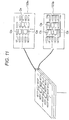
- Fig. 12 shows a basic configuration of a connector applied to a second embodiment of the control apparatus according to the present invention.
- the second embodiment is different from the first embodiment in the configuration of the connection terminals of the connector, but is the same as the first embodiment in the other configuration. Therefore, the same components as in the first embodiment are assigned the same reference signs, and the detailed description is omitted.
- connection terminals 111A which connect a printed circuit board to an external device and external wires are formed of conductive materials 125aA and 125bA, where the conductive materials 125aA and 125bA are made to fill through-holes 121aA and 121bA and are solidified, and the through-holes 121aA and 121bA are formed, in the lamination direction, at the positions corresponding to terminal connecting patterns of a terminal circuit pattern and to a ground part of a ground pattern of a ground circuit pattern.
- the conductive materials 125aA and 125bA made to fill the through-holes 121aA and 121bA are formed to be approximately flush with the surface of a laminated ceramic capacitor 113A.
- molten conductive material made of, for example, solder or the like is made to fill the through-holes 121aA and 121bA formed, in the lamination direction, at the positions corresponding to the terminal connecting patterns of the terminal circuit pattern and the ground part of the ground pattern of the ground circuit pattern, and is solidified in a predetermined atmosphere, so that the connection terminals 111A are formed which are input/output terminals 111aA formed of the conductive materials 125aA and a ground terminal 111bA formed of the conductive material 125bA, where the surfaces of the connection terminals 111A are approximately flush with the surface of the laminated ceramic capacitor 113A.
- connection terminals 111A such as the input/output terminals 111aA and the ground terminal 111bA are formed of the conductive materials 125aA and 125bA made to fill the through-holes 121aA and 121bA, so that it is easy to manufacture the connector which is equipped with the connection terminals having the surfaces which are approximately flush with the surface of the laminated ceramic capacitor 113A used for, for example, a USB connector or the like, whereby an application field of the connector 110A can be enlarged.
- a female connector M corresponding to the male connector 110A shown in Fig. 12 can be manufactured by forming, in dielectric material made of ceramic or the like, through-holes MaA and MbA at the positions corresponding to the through-holes 121aA and 121bA of the connector 110A as shown in Fig. 13 , and by filling the through-holes MaA and MbA with conductive material for forming connection terminals and then solidifying the conductive material, or by fitting into the through-holes MaA and MbA metal pins for connection which are to form connection terminals.
- Fig. 14 shows a basic configuration of a connector applied to a third embodiment of the control apparatus according to the present invention.
- the third embodiment is different from the first and second embodiments in the configuration of the connection terminals of the connector and the circuit pattern printed on the surface, but is the same as the first and second embodiments in the other configuration. Therefore, the detailed description of the same configuration to the first and second embodiments is omitted.
- a connector 110B shown in Fig. 14 is a contact type connector to be used for, for example, a USB connector and the like, and the connector 110B is formed, similarly to the above second embodiment, such that through-holes 121aB and 121bB are formed, in a lamination direction of a laminated ceramic capacitor 113B, at positions corresponding to terminal connecting patterns of a terminal circuit pattern printed on a terminal dielectric sheet and at positions corresponding to a ground part of a ground pattern of a ground circuit pattern printed on a ground dielectric sheet, and that in the through-holes 121aB and 121bB, conductive materials 125aB and 125bB made of, for example, solder or the like are made to fill and are solidified, and there are formed parts of input/output terminals 111aB and a ground terminal 111bB forming connection terminals 111B.
- the contact terminals 126aB arranged on the one side edge of the surface of the connector 110B and conductive materials 125aB made to fill the through-holes 121aB are electrically connected to each other through a circuit pattern 127aB additionally printed on the surface of the laminated ceramic capacitor 113B, so that the input/output terminals 111aB are formed of the conductive materials 125aB, the circuit pattern 127aB, and the contact terminals 126aB.
- the contact terminal 126bB arranged on the one side edge of the surface of the connector 110B and the conductive material 125bB made to fill a through-hole 121bB are electrically connected to each other through a circuit pattern 127bB additionally printed on the surface of the laminated ceramic capacitor 113B, so that the ground terminal 111bB is formed of the conductive material 125bB, the circuit pattern 127bB, and the contact terminal 126bB.
- the terminal connecting patterns of the terminal circuit pattern are electrically connected to the input/output terminals 111aB formed of the conductive materials 125aB made to fill the through-holes 121aB, the circuit pattern 127aB formed on the surface of the laminated ceramic capacitor 113B, and the contact terminals 126aB for input/output; and the ground pattern of the ground circuit pattern is electrically connected to the ground terminal 111bB formed of the conductive material 125bB made to fill the through-hole 121bB, the circuit pattern 127bB formed on the surface of the laminated capacitor 113B, and the contact terminal 126bB for ground.
- connection terminals 111B such as the input/output terminals 111aB and the ground terminal 111bB are formed of the conductive materials 125aB and 125bB made to fill the through-holes 121aB and 121bB, the circuit patterns 127aB and 127bB formed on the surface of the laminated capacitor 113B, and the contact terminals 126aB and 126bB arranged on the one side edge of the surface of the connector 110B; thus, it is easy to manufacture a contact type connector which is used for, for example, a USB connector or the like and which is small, light, and high capacitance, whereby the field of application of the connector 110B can be enlarged.
- the dielectric sheets forming the laminated ceramic capacitor is formed of barium titanate (BaTiO 3 ) to secure a capacitor capacitance; however, the dielectric sheet may be made of, for example, calcium titanate (CaTiO 3 ), strontium titanate (SrTiO 3 ), calcium zirconate (CaZrO 3 ), or the like.
- circuit pattern printed on the surface of the dielectric sheet and the surface of the laminated ceramic capacitor can be appropriately modified depending on required performances such as the number or the arrangement of the connection terminals.
- a shape and a size of a connector housing containing a laminated ceramic capacitor a position of disposition of a connector in a main body case or how to fix the connector; a position of disposition of a printed circuit board in a main body case or how to fix the printed circuit board; a position of disposition of an electronic component on a printed circuit board or how to fix the electronic component; and a type and a number of electronic component.
- the present invention is not limited to the first to third embodiments and includes various types of deformation.
- the first to third embodiments describe in detail for easy-to-understand description, but the present invention does not need to be equipped with all the described components.
- another component can be added, removed, and replaced.
- control lines and information lines the lines which are thought to be necessary for description are shown, and not all the control lines and the information lines which are necessary as a product are shown. It can be thought that almost all the components are actually connected to each other.
Landscapes
- Engineering & Computer Science (AREA)
- Power Engineering (AREA)
- Microelectronics & Electronic Packaging (AREA)
- Manufacturing & Machinery (AREA)
- Chemical & Material Sciences (AREA)
- Ceramic Engineering (AREA)
- Inorganic Chemistry (AREA)
- Fixed Capacitors And Capacitor Manufacturing Machines (AREA)
- Details Of Connecting Devices For Male And Female Coupling (AREA)
- Structures For Mounting Electric Components On Printed Circuit Boards (AREA)
- Coupling Device And Connection With Printed Circuit (AREA)
Applications Claiming Priority (2)
| Application Number | Priority Date | Filing Date | Title |
|---|---|---|---|
| JP2013108172A JP6129643B2 (ja) | 2013-05-22 | 2013-05-22 | 制御装置、コネクタ、及びコネクタ用積層コンデンサ |
| PCT/JP2014/056100 WO2014188758A1 (ja) | 2013-05-22 | 2014-03-10 | 制御装置、コネクタ、及びコネクタ用積層コンデンサ |
Publications (3)
| Publication Number | Publication Date |
|---|---|
| EP3000664A1 EP3000664A1 (en) | 2016-03-30 |
| EP3000664A4 EP3000664A4 (en) | 2018-03-28 |
| EP3000664B1 true EP3000664B1 (en) | 2020-09-23 |
Family
ID=51933324
Family Applications (1)
| Application Number | Title | Priority Date | Filing Date |
|---|---|---|---|
| EP14801888.0A Active EP3000664B1 (en) | 2013-05-22 | 2014-03-10 | Control apparatus, connector, and laminated capacitor for connector |
Country Status (5)
| Country | Link |
|---|---|
| US (1) | US9705261B2 (ja) |
| EP (1) | EP3000664B1 (ja) |
| JP (1) | JP6129643B2 (ja) |
| CN (1) | CN105228863B (ja) |
| WO (1) | WO2014188758A1 (ja) |
Cited By (1)
| Publication number | Priority date | Publication date | Assignee | Title |
|---|---|---|---|---|
| EP4618323A4 (en) * | 2023-01-06 | 2026-03-04 | Samsung Electronics Co Ltd | CONNECTOR ASSEMBLY |
Families Citing this family (4)
| Publication number | Priority date | Publication date | Assignee | Title |
|---|---|---|---|---|
| JP6129643B2 (ja) * | 2013-05-22 | 2017-05-17 | 日立オートモティブシステムズ株式会社 | 制御装置、コネクタ、及びコネクタ用積層コンデンサ |
| US9680261B2 (en) * | 2014-06-11 | 2017-06-13 | Honewell International Inc. | Intrinsic safe in-line adaptor with integrated capacitive barrier for connecting a wireless module with antenna |
| KR101792381B1 (ko) * | 2016-01-04 | 2017-11-01 | 삼성전기주식회사 | 전자부품 및 그 제조방법 |
| CA3246649A1 (en) * | 2022-04-22 | 2023-10-26 | Rheem Manufacturing Company | Plug-in connector with an authentication feature |
Family Cites Families (20)
| Publication number | Priority date | Publication date | Assignee | Title |
|---|---|---|---|---|
| JPH05234643A (ja) | 1992-02-21 | 1993-09-10 | Tdk Corp | ノイズ対策型コネクタおよび同コネクタ用ノイズ除去部品 |
| US5580279A (en) * | 1994-10-31 | 1996-12-03 | Berg Technology, Inc. | Low cost filtered and shielded electronic connector and method of use |
| US5905627A (en) * | 1997-09-10 | 1999-05-18 | Maxwell Energy Products, Inc. | Internally grounded feedthrough filter capacitor |
| US6165018A (en) * | 1999-04-27 | 2000-12-26 | Lucent Technologies Inc. | Connector having internal crosstalk compensation |
| JP2001307910A (ja) * | 2000-04-25 | 2001-11-02 | Tdk Corp | 積層電子部品アレイ |
| US6882248B2 (en) * | 2000-09-07 | 2005-04-19 | Greatbatch-Sierra, Inc. | EMI filtered connectors using internally grounded feedthrough capacitors |
| DE10233318C1 (de) * | 2002-07-22 | 2003-09-25 | Siemens Ag | Entstöreinrichtung |
| JP2005310531A (ja) * | 2004-04-21 | 2005-11-04 | Auto Network Gijutsu Kenkyusho:Kk | 電気機器 |
| JP4960583B2 (ja) * | 2004-07-07 | 2012-06-27 | Tdk株式会社 | 積層型lc複合部品 |
| KR100678083B1 (ko) * | 2004-11-11 | 2007-02-02 | 삼성전자주식회사 | 임베디드 캐패시터와 임베디드 캐패시터의 제작 방법 |
| EP1760735B1 (en) * | 2005-09-02 | 2015-03-11 | Greatbatch Ltd. | Screen-printed capacitors for filter feedthrough assemblies |
| US7564674B2 (en) * | 2005-12-12 | 2009-07-21 | Greatbatch Ltd. | Feedthrough filter capacitor assemblies having low cost terminal pins |
| JP4851243B2 (ja) | 2006-03-20 | 2012-01-11 | 株式会社オートネットワーク技術研究所 | コンデンサ内蔵ジョイントコネクタ |
| EP2259669A4 (en) * | 2008-03-24 | 2011-12-28 | Ngk Spark Plug Co | COMPONENT WITH PCB |
| CN102196703B (zh) | 2010-03-16 | 2015-10-14 | 日立汽车系统株式会社 | 电子设备 |
| JP5174071B2 (ja) | 2010-03-16 | 2013-04-03 | 日立オートモティブシステムズ株式会社 | 電子機器装置 |
| EP2398026B1 (en) * | 2010-06-15 | 2019-08-21 | Greatbatch Ltd. | Coating of non-solderable base metal for soldering application in medical device component |
| US8642887B1 (en) * | 2010-12-03 | 2014-02-04 | Greatbatch Ltd. | Metallization barrier for a hermetic feedthrough |
| EP2529790B1 (en) * | 2011-06-03 | 2017-09-20 | Greatbatch Ltd. | Feedthrough wire connector for use in a medical device |
| JP6129643B2 (ja) * | 2013-05-22 | 2017-05-17 | 日立オートモティブシステムズ株式会社 | 制御装置、コネクタ、及びコネクタ用積層コンデンサ |
-
2013
- 2013-05-22 JP JP2013108172A patent/JP6129643B2/ja active Active
-
2014
- 2014-03-10 US US14/787,338 patent/US9705261B2/en active Active
- 2014-03-10 EP EP14801888.0A patent/EP3000664B1/en active Active
- 2014-03-10 CN CN201480028626.1A patent/CN105228863B/zh active Active
- 2014-03-10 WO PCT/JP2014/056100 patent/WO2014188758A1/ja not_active Ceased
Non-Patent Citations (1)
| Title |
|---|
| None * |
Cited By (1)
| Publication number | Priority date | Publication date | Assignee | Title |
|---|---|---|---|---|
| EP4618323A4 (en) * | 2023-01-06 | 2026-03-04 | Samsung Electronics Co Ltd | CONNECTOR ASSEMBLY |
Also Published As
| Publication number | Publication date |
|---|---|
| EP3000664A1 (en) | 2016-03-30 |
| US20160072228A1 (en) | 2016-03-10 |
| WO2014188758A1 (ja) | 2014-11-27 |
| EP3000664A4 (en) | 2018-03-28 |
| CN105228863A (zh) | 2016-01-06 |
| JP2014227039A (ja) | 2014-12-08 |
| CN105228863B (zh) | 2017-05-10 |
| US9705261B2 (en) | 2017-07-11 |
| JP6129643B2 (ja) | 2017-05-17 |
Similar Documents
| Publication | Publication Date | Title |
|---|---|---|
| EP3000664B1 (en) | Control apparatus, connector, and laminated capacitor for connector | |
| US9648746B2 (en) | Composite electronic component and board having the same | |
| US5796572A (en) | Thin film capacitor and hybrid circuit board and methods of producing same | |
| CN108364785B (zh) | 层叠电容器及电子部件装置 | |
| KR102139759B1 (ko) | 적층 세라믹 전자 부품 | |
| US7589953B2 (en) | Multilayer capacitor | |
| US20130134835A1 (en) | Ultrasonic sensor and manufacturing method thereof | |
| US10366839B1 (en) | Electronic component | |
| KR102516764B1 (ko) | 복합 전자 부품 | |
| JP2009053141A (ja) | 加速度センサモジュール | |
| CN103167748A (zh) | 电路板的制造方法 | |
| US20180233286A1 (en) | Capacitor component and method of manufacturing the same | |
| US20060030216A1 (en) | Connector housing | |
| JP2000286526A (ja) | 表面実装構造及びその表面実装構造に用いられる表面実装型電子部品 | |
| CN109427484B (zh) | 电容器组件 | |
| CN106796844B (zh) | 叠层电容器及车载控制装置 | |
| KR20190121221A (ko) | 전자 부품 | |
| US20090154122A1 (en) | Mechanical component-containing board and method of manufacturing same | |
| US20210168950A1 (en) | Electronic device and electric power steering apparatus having electronic device mounted thereto | |
| US11302483B2 (en) | Electronic component | |
| JP4942776B2 (ja) | 電子デバイスパッケージ構造及びそれが用いられた電子回路モジュール | |
| JP2011061044A (ja) | 多層基板のサージ除去構造および車載用電子機器 | |
| KR20210075672A (ko) | 전자 부품 | |
| CN104240943A (zh) | 多层陶瓷电子部件及其制造方法 | |
| JP3591915B2 (ja) | 積層電子部品 |
Legal Events
| Date | Code | Title | Description |
|---|---|---|---|
| PUAI | Public reference made under article 153(3) epc to a published international application that has entered the european phase |
Free format text: ORIGINAL CODE: 0009012 |
|
| 17P | Request for examination filed |
Effective date: 20151222 |
|
| AK | Designated contracting states |
Kind code of ref document: A1 Designated state(s): AL AT BE BG CH CY CZ DE DK EE ES FI FR GB GR HR HU IE IS IT LI LT LU LV MC MK MT NL NO PL PT RO RS SE SI SK SM TR |
|
| AX | Request for extension of the european patent |
Extension state: BA ME |
|
| DAX | Request for extension of the european patent (deleted) | ||
| A4 | Supplementary search report drawn up and despatched |
Effective date: 20180227 |
|
| RIC1 | Information provided on ipc code assigned before grant |
Ipc: H01G 2/06 20060101ALI20180221BHEP Ipc: H01R 13/6466 20110101ALI20180221BHEP Ipc: H05K 1/18 20060101ALI20180221BHEP Ipc: H01G 4/40 20060101ALI20180221BHEP Ipc: H01R 13/66 20060101ALI20180221BHEP Ipc: H01G 4/232 20060101ALI20180221BHEP Ipc: H01G 4/30 20060101AFI20180221BHEP Ipc: H01G 4/38 20060101ALI20180221BHEP |
|
| REG | Reference to a national code |
Ref country code: DE Ref legal event code: R079 Ref document number: 602014070538 Country of ref document: DE Free format text: PREVIOUS MAIN CLASS: B60R0016020000 Ipc: H01G0004300000 |
|
| GRAP | Despatch of communication of intention to grant a patent |
Free format text: ORIGINAL CODE: EPIDOSNIGR1 |
|
| STAA | Information on the status of an ep patent application or granted ep patent |
Free format text: STATUS: GRANT OF PATENT IS INTENDED |
|
| RIC1 | Information provided on ipc code assigned before grant |
Ipc: H01G 4/40 20060101ALI20200409BHEP Ipc: H01R 13/66 20060101ALI20200409BHEP Ipc: H01G 4/30 20060101AFI20200409BHEP Ipc: H01G 4/38 20060101ALI20200409BHEP Ipc: H01G 4/232 20060101ALI20200409BHEP Ipc: H01G 2/06 20060101ALI20200409BHEP Ipc: H01R 13/6466 20110101ALI20200409BHEP Ipc: H05K 1/18 20060101ALI20200409BHEP |
|
| INTG | Intention to grant announced |
Effective date: 20200424 |
|
| RIN1 | Information on inventor provided before grant (corrected) |
Inventor name: SHIH, HSINHAN |
|
| GRAS | Grant fee paid |
Free format text: ORIGINAL CODE: EPIDOSNIGR3 |
|
| GRAA | (expected) grant |
Free format text: ORIGINAL CODE: 0009210 |
|
| STAA | Information on the status of an ep patent application or granted ep patent |
Free format text: STATUS: THE PATENT HAS BEEN GRANTED |
|
| AK | Designated contracting states |
Kind code of ref document: B1 Designated state(s): AL AT BE BG CH CY CZ DE DK EE ES FI FR GB GR HR HU IE IS IT LI LT LU LV MC MK MT NL NO PL PT RO RS SE SI SK SM TR |
|
| REG | Reference to a national code |
Ref country code: GB Ref legal event code: FG4D |
|
| REG | Reference to a national code |
Ref country code: CH Ref legal event code: EP |
|
| REG | Reference to a national code |
Ref country code: IE Ref legal event code: FG4D |
|
| REG | Reference to a national code |
Ref country code: DE Ref legal event code: R096 Ref document number: 602014070538 Country of ref document: DE Ref country code: AT Ref legal event code: REF Ref document number: 1317219 Country of ref document: AT Kind code of ref document: T Effective date: 20201015 |
|
| PG25 | Lapsed in a contracting state [announced via postgrant information from national office to epo] |
Ref country code: FI Free format text: LAPSE BECAUSE OF FAILURE TO SUBMIT A TRANSLATION OF THE DESCRIPTION OR TO PAY THE FEE WITHIN THE PRESCRIBED TIME-LIMIT Effective date: 20200923 Ref country code: HR Free format text: LAPSE BECAUSE OF FAILURE TO SUBMIT A TRANSLATION OF THE DESCRIPTION OR TO PAY THE FEE WITHIN THE PRESCRIBED TIME-LIMIT Effective date: 20200923 Ref country code: BG Free format text: LAPSE BECAUSE OF FAILURE TO SUBMIT A TRANSLATION OF THE DESCRIPTION OR TO PAY THE FEE WITHIN THE PRESCRIBED TIME-LIMIT Effective date: 20201223 Ref country code: SE Free format text: LAPSE BECAUSE OF FAILURE TO SUBMIT A TRANSLATION OF THE DESCRIPTION OR TO PAY THE FEE WITHIN THE PRESCRIBED TIME-LIMIT Effective date: 20200923 Ref country code: GR Free format text: LAPSE BECAUSE OF FAILURE TO SUBMIT A TRANSLATION OF THE DESCRIPTION OR TO PAY THE FEE WITHIN THE PRESCRIBED TIME-LIMIT Effective date: 20201224 Ref country code: NO Free format text: LAPSE BECAUSE OF FAILURE TO SUBMIT A TRANSLATION OF THE DESCRIPTION OR TO PAY THE FEE WITHIN THE PRESCRIBED TIME-LIMIT Effective date: 20201223 |
|
| REG | Reference to a national code |
Ref country code: AT Ref legal event code: MK05 Ref document number: 1317219 Country of ref document: AT Kind code of ref document: T Effective date: 20200923 |
|
| PG25 | Lapsed in a contracting state [announced via postgrant information from national office to epo] |
Ref country code: RS Free format text: LAPSE BECAUSE OF FAILURE TO SUBMIT A TRANSLATION OF THE DESCRIPTION OR TO PAY THE FEE WITHIN THE PRESCRIBED TIME-LIMIT Effective date: 20200923 Ref country code: LV Free format text: LAPSE BECAUSE OF FAILURE TO SUBMIT A TRANSLATION OF THE DESCRIPTION OR TO PAY THE FEE WITHIN THE PRESCRIBED TIME-LIMIT Effective date: 20200923 |
|
| REG | Reference to a national code |
Ref country code: NL Ref legal event code: MP Effective date: 20200923 |
|
| REG | Reference to a national code |
Ref country code: DE Ref legal event code: R082 Ref document number: 602014070538 Country of ref document: DE Representative=s name: MERH-IP MATIAS ERNY REICHL HOFFMANN PATENTANWA, DE Ref country code: DE Ref legal event code: R081 Ref document number: 602014070538 Country of ref document: DE Owner name: HITACHI ASTEMO, LTD., HITACHINAKA-SHI, JP Free format text: FORMER OWNER: HITACHI AUTOMOTIVE SYSTEMS, LTD., HITACHINAKA-SHI, IBARAKI, JP |
|
| REG | Reference to a national code |
Ref country code: LT Ref legal event code: MG4D |
|
| PG25 | Lapsed in a contracting state [announced via postgrant information from national office to epo] |
Ref country code: CZ Free format text: LAPSE BECAUSE OF FAILURE TO SUBMIT A TRANSLATION OF THE DESCRIPTION OR TO PAY THE FEE WITHIN THE PRESCRIBED TIME-LIMIT Effective date: 20200923 Ref country code: PT Free format text: LAPSE BECAUSE OF FAILURE TO SUBMIT A TRANSLATION OF THE DESCRIPTION OR TO PAY THE FEE WITHIN THE PRESCRIBED TIME-LIMIT Effective date: 20210125 Ref country code: LT Free format text: LAPSE BECAUSE OF FAILURE TO SUBMIT A TRANSLATION OF THE DESCRIPTION OR TO PAY THE FEE WITHIN THE PRESCRIBED TIME-LIMIT Effective date: 20200923 Ref country code: NL Free format text: LAPSE BECAUSE OF FAILURE TO SUBMIT A TRANSLATION OF THE DESCRIPTION OR TO PAY THE FEE WITHIN THE PRESCRIBED TIME-LIMIT Effective date: 20200923 Ref country code: RO Free format text: LAPSE BECAUSE OF FAILURE TO SUBMIT A TRANSLATION OF THE DESCRIPTION OR TO PAY THE FEE WITHIN THE PRESCRIBED TIME-LIMIT Effective date: 20200923 Ref country code: SM Free format text: LAPSE BECAUSE OF FAILURE TO SUBMIT A TRANSLATION OF THE DESCRIPTION OR TO PAY THE FEE WITHIN THE PRESCRIBED TIME-LIMIT Effective date: 20200923 Ref country code: EE Free format text: LAPSE BECAUSE OF FAILURE TO SUBMIT A TRANSLATION OF THE DESCRIPTION OR TO PAY THE FEE WITHIN THE PRESCRIBED TIME-LIMIT Effective date: 20200923 |
|
| PG25 | Lapsed in a contracting state [announced via postgrant information from national office to epo] |
Ref country code: ES Free format text: LAPSE BECAUSE OF FAILURE TO SUBMIT A TRANSLATION OF THE DESCRIPTION OR TO PAY THE FEE WITHIN THE PRESCRIBED TIME-LIMIT Effective date: 20200923 Ref country code: AL Free format text: LAPSE BECAUSE OF FAILURE TO SUBMIT A TRANSLATION OF THE DESCRIPTION OR TO PAY THE FEE WITHIN THE PRESCRIBED TIME-LIMIT Effective date: 20200923 Ref country code: AT Free format text: LAPSE BECAUSE OF FAILURE TO SUBMIT A TRANSLATION OF THE DESCRIPTION OR TO PAY THE FEE WITHIN THE PRESCRIBED TIME-LIMIT Effective date: 20200923 Ref country code: PL Free format text: LAPSE BECAUSE OF FAILURE TO SUBMIT A TRANSLATION OF THE DESCRIPTION OR TO PAY THE FEE WITHIN THE PRESCRIBED TIME-LIMIT Effective date: 20200923 Ref country code: IS Free format text: LAPSE BECAUSE OF FAILURE TO SUBMIT A TRANSLATION OF THE DESCRIPTION OR TO PAY THE FEE WITHIN THE PRESCRIBED TIME-LIMIT Effective date: 20210123 |
|
| REG | Reference to a national code |
Ref country code: DE Ref legal event code: R097 Ref document number: 602014070538 Country of ref document: DE |
|
| PG25 | Lapsed in a contracting state [announced via postgrant information from national office to epo] |
Ref country code: SK Free format text: LAPSE BECAUSE OF FAILURE TO SUBMIT A TRANSLATION OF THE DESCRIPTION OR TO PAY THE FEE WITHIN THE PRESCRIBED TIME-LIMIT Effective date: 20200923 |
|
| PLBE | No opposition filed within time limit |
Free format text: ORIGINAL CODE: 0009261 |
|
| STAA | Information on the status of an ep patent application or granted ep patent |
Free format text: STATUS: NO OPPOSITION FILED WITHIN TIME LIMIT |
|
| PG25 | Lapsed in a contracting state [announced via postgrant information from national office to epo] |
Ref country code: DK Free format text: LAPSE BECAUSE OF FAILURE TO SUBMIT A TRANSLATION OF THE DESCRIPTION OR TO PAY THE FEE WITHIN THE PRESCRIBED TIME-LIMIT Effective date: 20200923 Ref country code: SI Free format text: LAPSE BECAUSE OF FAILURE TO SUBMIT A TRANSLATION OF THE DESCRIPTION OR TO PAY THE FEE WITHIN THE PRESCRIBED TIME-LIMIT Effective date: 20200923 |
|
| 26N | No opposition filed |
Effective date: 20210624 |
|
| PG25 | Lapsed in a contracting state [announced via postgrant information from national office to epo] |
Ref country code: MC Free format text: LAPSE BECAUSE OF FAILURE TO SUBMIT A TRANSLATION OF THE DESCRIPTION OR TO PAY THE FEE WITHIN THE PRESCRIBED TIME-LIMIT Effective date: 20200923 Ref country code: IT Free format text: LAPSE BECAUSE OF FAILURE TO SUBMIT A TRANSLATION OF THE DESCRIPTION OR TO PAY THE FEE WITHIN THE PRESCRIBED TIME-LIMIT Effective date: 20200923 |
|
| REG | Reference to a national code |
Ref country code: CH Ref legal event code: PL |
|
| GBPC | Gb: european patent ceased through non-payment of renewal fee |
Effective date: 20210310 |
|
| REG | Reference to a national code |
Ref country code: BE Ref legal event code: MM Effective date: 20210331 |
|
| PG25 | Lapsed in a contracting state [announced via postgrant information from national office to epo] |
Ref country code: GB Free format text: LAPSE BECAUSE OF NON-PAYMENT OF DUE FEES Effective date: 20210310 Ref country code: IE Free format text: LAPSE BECAUSE OF NON-PAYMENT OF DUE FEES Effective date: 20210310 Ref country code: FR Free format text: LAPSE BECAUSE OF NON-PAYMENT OF DUE FEES Effective date: 20210331 Ref country code: LI Free format text: LAPSE BECAUSE OF NON-PAYMENT OF DUE FEES Effective date: 20210331 Ref country code: LU Free format text: LAPSE BECAUSE OF NON-PAYMENT OF DUE FEES Effective date: 20210310 Ref country code: CH Free format text: LAPSE BECAUSE OF NON-PAYMENT OF DUE FEES Effective date: 20210331 |
|
| PG25 | Lapsed in a contracting state [announced via postgrant information from national office to epo] |
Ref country code: BE Free format text: LAPSE BECAUSE OF NON-PAYMENT OF DUE FEES Effective date: 20210331 |
|
| PG25 | Lapsed in a contracting state [announced via postgrant information from national office to epo] |
Ref country code: HU Free format text: LAPSE BECAUSE OF FAILURE TO SUBMIT A TRANSLATION OF THE DESCRIPTION OR TO PAY THE FEE WITHIN THE PRESCRIBED TIME-LIMIT; INVALID AB INITIO Effective date: 20140310 |
|
| PG25 | Lapsed in a contracting state [announced via postgrant information from national office to epo] |
Ref country code: CY Free format text: LAPSE BECAUSE OF FAILURE TO SUBMIT A TRANSLATION OF THE DESCRIPTION OR TO PAY THE FEE WITHIN THE PRESCRIBED TIME-LIMIT Effective date: 20200923 |
|
| PG25 | Lapsed in a contracting state [announced via postgrant information from national office to epo] |
Ref country code: MK Free format text: LAPSE BECAUSE OF FAILURE TO SUBMIT A TRANSLATION OF THE DESCRIPTION OR TO PAY THE FEE WITHIN THE PRESCRIBED TIME-LIMIT Effective date: 20200923 |
|
| PG25 | Lapsed in a contracting state [announced via postgrant information from national office to epo] |
Ref country code: TR Free format text: LAPSE BECAUSE OF FAILURE TO SUBMIT A TRANSLATION OF THE DESCRIPTION OR TO PAY THE FEE WITHIN THE PRESCRIBED TIME-LIMIT Effective date: 20200923 |
|
| PG25 | Lapsed in a contracting state [announced via postgrant information from national office to epo] |
Ref country code: MT Free format text: LAPSE BECAUSE OF FAILURE TO SUBMIT A TRANSLATION OF THE DESCRIPTION OR TO PAY THE FEE WITHIN THE PRESCRIBED TIME-LIMIT Effective date: 20200923 |
|
| PGFP | Annual fee paid to national office [announced via postgrant information from national office to epo] |
Ref country code: DE Payment date: 20260128 Year of fee payment: 13 |