EP3010043B1 - Halbleiterbauelement und herstellungsverfahren dafür - Google Patents
Halbleiterbauelement und herstellungsverfahren dafür Download PDFInfo
- Publication number
- EP3010043B1 EP3010043B1 EP14807330.7A EP14807330A EP3010043B1 EP 3010043 B1 EP3010043 B1 EP 3010043B1 EP 14807330 A EP14807330 A EP 14807330A EP 3010043 B1 EP3010043 B1 EP 3010043B1
- Authority
- EP
- European Patent Office
- Prior art keywords
- electrode
- semiconductor device
- layer
- groove
- shape controlling
- Prior art date
- Legal status (The legal status is an assumption and is not a legal conclusion. Google has not performed a legal analysis and makes no representation as to the accuracy of the status listed.)
- Active
Links
Images






Classifications
-
- H—ELECTRICITY
- H10—SEMICONDUCTOR DEVICES; ELECTRIC SOLID-STATE DEVICES NOT OTHERWISE PROVIDED FOR
- H10D—INORGANIC ELECTRIC SEMICONDUCTOR DEVICES
- H10D64/00—Electrodes of devices having potential barriers
- H10D64/111—Field plates
-
- H—ELECTRICITY
- H10—SEMICONDUCTOR DEVICES; ELECTRIC SOLID-STATE DEVICES NOT OTHERWISE PROVIDED FOR
- H10D—INORGANIC ELECTRIC SEMICONDUCTOR DEVICES
- H10D30/00—Field-effect transistors [FET]
- H10D30/01—Manufacture or treatment
- H10D30/015—Manufacture or treatment of FETs having heterojunction interface channels or heterojunction gate electrodes, e.g. HEMT
-
- H—ELECTRICITY
- H10—SEMICONDUCTOR DEVICES; ELECTRIC SOLID-STATE DEVICES NOT OTHERWISE PROVIDED FOR
- H10D—INORGANIC ELECTRIC SEMICONDUCTOR DEVICES
- H10D30/00—Field-effect transistors [FET]
- H10D30/01—Manufacture or treatment
- H10D30/021—Manufacture or treatment of FETs having insulated gates [IGFET]
- H10D30/028—Manufacture or treatment of FETs having insulated gates [IGFET] of double-diffused metal oxide semiconductor [DMOS] FETs
- H10D30/0281—Manufacture or treatment of FETs having insulated gates [IGFET] of double-diffused metal oxide semiconductor [DMOS] FETs of lateral DMOS [LDMOS] FETs
-
- H—ELECTRICITY
- H10—SEMICONDUCTOR DEVICES; ELECTRIC SOLID-STATE DEVICES NOT OTHERWISE PROVIDED FOR
- H10D—INORGANIC ELECTRIC SEMICONDUCTOR DEVICES
- H10D30/00—Field-effect transistors [FET]
- H10D30/40—FETs having zero-dimensional [0D], one-dimensional [1D] or two-dimensional [2D] charge carrier gas channels
- H10D30/47—FETs having zero-dimensional [0D], one-dimensional [1D] or two-dimensional [2D] charge carrier gas channels having two-dimensional [2D] charge carrier gas channels, e.g. nanoribbon FETs or high electron mobility transistors [HEMT]
- H10D30/471—High electron mobility transistors [HEMT] or high hole mobility transistors [HHMT]
- H10D30/475—High electron mobility transistors [HEMT] or high hole mobility transistors [HHMT] having wider bandgap layer formed on top of lower bandgap active layer, e.g. undoped barrier HEMTs such as i-AlGaN/GaN HEMTs
- H10D30/4755—High electron mobility transistors [HEMT] or high hole mobility transistors [HHMT] having wider bandgap layer formed on top of lower bandgap active layer, e.g. undoped barrier HEMTs such as i-AlGaN/GaN HEMTs having wide bandgap charge-carrier supplying layers, e.g. modulation doped HEMTs such as n-AlGaAs/GaAs HEMTs
-
- H—ELECTRICITY
- H10—SEMICONDUCTOR DEVICES; ELECTRIC SOLID-STATE DEVICES NOT OTHERWISE PROVIDED FOR
- H10D—INORGANIC ELECTRIC SEMICONDUCTOR DEVICES
- H10D30/00—Field-effect transistors [FET]
- H10D30/60—Insulated-gate field-effect transistors [IGFET]
- H10D30/64—Double-diffused metal-oxide semiconductor [DMOS] FETs
- H10D30/65—Lateral DMOS [LDMOS] FETs
- H10D30/655—Lateral DMOS [LDMOS] FETs having edge termination structures
-
- H—ELECTRICITY
- H10—SEMICONDUCTOR DEVICES; ELECTRIC SOLID-STATE DEVICES NOT OTHERWISE PROVIDED FOR
- H10D—INORGANIC ELECTRIC SEMICONDUCTOR DEVICES
- H10D30/00—Field-effect transistors [FET]
- H10D30/60—Insulated-gate field-effect transistors [IGFET]
- H10D30/69—IGFETs having charge trapping gate insulators, e.g. MNOS transistors
- H10D30/694—IGFETs having charge trapping gate insulators, e.g. MNOS transistors characterised by the shapes, relative sizes or dispositions of the gate electrodes
- H10D30/699—IGFETs having charge trapping gate insulators, e.g. MNOS transistors characterised by the shapes, relative sizes or dispositions of the gate electrodes having the gate at least partly formed in a trench
-
- H—ELECTRICITY
- H10—SEMICONDUCTOR DEVICES; ELECTRIC SOLID-STATE DEVICES NOT OTHERWISE PROVIDED FOR
- H10D—INORGANIC ELECTRIC SEMICONDUCTOR DEVICES
- H10D62/00—Semiconductor bodies, or regions thereof, of devices having potential barriers
- H10D62/80—Semiconductor bodies, or regions thereof, of devices having potential barriers characterised by the materials
- H10D62/85—Semiconductor bodies, or regions thereof, of devices having potential barriers characterised by the materials being Group III-V materials, e.g. GaAs
- H10D62/8503—Nitride Group III-V materials, e.g. AlN or GaN
-
- H—ELECTRICITY
- H10—SEMICONDUCTOR DEVICES; ELECTRIC SOLID-STATE DEVICES NOT OTHERWISE PROVIDED FOR
- H10D—INORGANIC ELECTRIC SEMICONDUCTOR DEVICES
- H10D64/00—Electrodes of devices having potential barriers
- H10D64/01—Manufacture or treatment
- H10D64/031—Manufacture or treatment of data-storage electrodes
- H10D64/035—Manufacture or treatment of data-storage electrodes comprising conductor-insulator-conductor-insulator-semiconductor structures
-
- H—ELECTRICITY
- H10—SEMICONDUCTOR DEVICES; ELECTRIC SOLID-STATE DEVICES NOT OTHERWISE PROVIDED FOR
- H10D—INORGANIC ELECTRIC SEMICONDUCTOR DEVICES
- H10D64/00—Electrodes of devices having potential barriers
- H10D64/20—Electrodes characterised by their shapes, relative sizes or dispositions
-
- H—ELECTRICITY
- H10—SEMICONDUCTOR DEVICES; ELECTRIC SOLID-STATE DEVICES NOT OTHERWISE PROVIDED FOR
- H10D—INORGANIC ELECTRIC SEMICONDUCTOR DEVICES
- H10D64/00—Electrodes of devices having potential barriers
- H10D64/20—Electrodes characterised by their shapes, relative sizes or dispositions
- H10D64/23—Electrodes carrying the current to be rectified, amplified, oscillated or switched, e.g. sources, drains, anodes or cathodes
-
- H—ELECTRICITY
- H10—SEMICONDUCTOR DEVICES; ELECTRIC SOLID-STATE DEVICES NOT OTHERWISE PROVIDED FOR
- H10D—INORGANIC ELECTRIC SEMICONDUCTOR DEVICES
- H10D64/00—Electrodes of devices having potential barriers
- H10D64/20—Electrodes characterised by their shapes, relative sizes or dispositions
- H10D64/23—Electrodes carrying the current to be rectified, amplified, oscillated or switched, e.g. sources, drains, anodes or cathodes
- H10D64/251—Source or drain electrodes for field-effect devices
-
- H—ELECTRICITY
- H10—SEMICONDUCTOR DEVICES; ELECTRIC SOLID-STATE DEVICES NOT OTHERWISE PROVIDED FOR
- H10D—INORGANIC ELECTRIC SEMICONDUCTOR DEVICES
- H10D64/00—Electrodes of devices having potential barriers
- H10D64/20—Electrodes characterised by their shapes, relative sizes or dispositions
- H10D64/27—Electrodes not carrying the current to be rectified, amplified, oscillated or switched, e.g. gates
- H10D64/311—Gate electrodes for field-effect devices
- H10D64/411—Gate electrodes for field-effect devices for FETs
- H10D64/511—Gate electrodes for field-effect devices for FETs for IGFETs
- H10D64/512—Disposition of the gate electrodes, e.g. buried gates
-
- H—ELECTRICITY
- H10—SEMICONDUCTOR DEVICES; ELECTRIC SOLID-STATE DEVICES NOT OTHERWISE PROVIDED FOR
- H10D—INORGANIC ELECTRIC SEMICONDUCTOR DEVICES
- H10D8/00—Diodes
- H10D8/01—Manufacture or treatment
- H10D8/045—Manufacture or treatment of PN junction diodes
-
- H—ELECTRICITY
- H10—SEMICONDUCTOR DEVICES; ELECTRIC SOLID-STATE DEVICES NOT OTHERWISE PROVIDED FOR
- H10D—INORGANIC ELECTRIC SEMICONDUCTOR DEVICES
- H10D8/00—Diodes
- H10D8/01—Manufacture or treatment
- H10D8/051—Manufacture or treatment of Schottky diodes
-
- H—ELECTRICITY
- H10—SEMICONDUCTOR DEVICES; ELECTRIC SOLID-STATE DEVICES NOT OTHERWISE PROVIDED FOR
- H10D—INORGANIC ELECTRIC SEMICONDUCTOR DEVICES
- H10D8/00—Diodes
- H10D8/411—PN diodes having planar bodies
-
- H—ELECTRICITY
- H10—SEMICONDUCTOR DEVICES; ELECTRIC SOLID-STATE DEVICES NOT OTHERWISE PROVIDED FOR
- H10D—INORGANIC ELECTRIC SEMICONDUCTOR DEVICES
- H10D8/00—Diodes
- H10D8/50—PIN diodes
-
- H—ELECTRICITY
- H10—SEMICONDUCTOR DEVICES; ELECTRIC SOLID-STATE DEVICES NOT OTHERWISE PROVIDED FOR
- H10D—INORGANIC ELECTRIC SEMICONDUCTOR DEVICES
- H10D8/00—Diodes
- H10D8/60—Schottky-barrier diodes
-
- H—ELECTRICITY
- H10—SEMICONDUCTOR DEVICES; ELECTRIC SOLID-STATE DEVICES NOT OTHERWISE PROVIDED FOR
- H10P—GENERIC PROCESSES OR APPARATUS FOR THE MANUFACTURE OR TREATMENT OF DEVICES COVERED BY CLASS H10
- H10P14/00—Formation of materials, e.g. in the shape of layers or pillars
- H10P14/40—Formation of materials, e.g. in the shape of layers or pillars of conductive or resistive materials
-
- H—ELECTRICITY
- H10—SEMICONDUCTOR DEVICES; ELECTRIC SOLID-STATE DEVICES NOT OTHERWISE PROVIDED FOR
- H10P—GENERIC PROCESSES OR APPARATUS FOR THE MANUFACTURE OR TREATMENT OF DEVICES COVERED BY CLASS H10
- H10P14/00—Formation of materials, e.g. in the shape of layers or pillars
- H10P14/60—Formation of materials, e.g. in the shape of layers or pillars of insulating materials
-
- H—ELECTRICITY
- H10—SEMICONDUCTOR DEVICES; ELECTRIC SOLID-STATE DEVICES NOT OTHERWISE PROVIDED FOR
- H10P—GENERIC PROCESSES OR APPARATUS FOR THE MANUFACTURE OR TREATMENT OF DEVICES COVERED BY CLASS H10
- H10P50/00—Etching of wafers, substrates or parts of devices
- H10P50/20—Dry etching; Plasma etching; Reactive-ion etching
- H10P50/28—Dry etching; Plasma etching; Reactive-ion etching of insulating materials
- H10P50/282—Dry etching; Plasma etching; Reactive-ion etching of insulating materials of inorganic materials
- H10P50/283—Dry etching; Plasma etching; Reactive-ion etching of insulating materials of inorganic materials by chemical means
-
- H—ELECTRICITY
- H10—SEMICONDUCTOR DEVICES; ELECTRIC SOLID-STATE DEVICES NOT OTHERWISE PROVIDED FOR
- H10P—GENERIC PROCESSES OR APPARATUS FOR THE MANUFACTURE OR TREATMENT OF DEVICES COVERED BY CLASS H10
- H10P50/00—Etching of wafers, substrates or parts of devices
- H10P50/71—Etching of wafers, substrates or parts of devices using masks for conductive or resistive materials
-
- H—ELECTRICITY
- H10—SEMICONDUCTOR DEVICES; ELECTRIC SOLID-STATE DEVICES NOT OTHERWISE PROVIDED FOR
- H10W—GENERIC PACKAGES, INTERCONNECTIONS, CONNECTORS OR OTHER CONSTRUCTIONAL DETAILS OF DEVICES COVERED BY CLASS H10
- H10W20/00—Interconnections in chips, wafers or substrates
- H10W20/01—Manufacture or treatment
- H10W20/071—Manufacture or treatment of dielectric parts thereof
- H10W20/081—Manufacture or treatment of dielectric parts thereof by forming openings in the dielectric parts
- H10W20/082—Manufacture or treatment of dielectric parts thereof by forming openings in the dielectric parts the openings being tapered via holes
Definitions
- the present invention relates to semiconductor technique, and more particularly to a semiconductor device and a manufacturing method therefor.
- Electric field distribution can be controlled by many ways, for example, modulating and doping active regions, adding field plates to reduce the maximum values of electric fields, and controlling shapes of electrodes to restrain electric field distribution.
- FIG. 1 shows distribution of electric field intensity between a source and a drain during operation of a GaN-based high electron mobility transistor. It could be seen that there is a very high electric field intensity at edges of the gate which are adjacent to the drain, the device will be breakdown once the peak electric field exceeds a critical electric field of the GaN material.
- the withstand voltage of the device is integration of the electric field intensity between the gate and the drain, compared with an electric field having uniform distribution, the higher the electric field intensity at the edges of the gate is, the smaller the withstand voltage is. This phenomenon will greatly degrade device performances, such as breakdown voltages and reliability of devices.
- LDMOS Laterally Diffused Metal Oxide Semiconductor
- MOSFET Metal-Oxide-Semiconductor Field-Effect Transistor
- UMOSFET U-shaped trench MOSFET
- the electric field at the edges also needs to be controlled.
- electric field distribution can be controlled by many ways, for example, modulating and doping active regions, using field plates to reduce the maximum values of electric fields, and controlling the shapes of the electrodes to restrain electric field distribution.
- Field plates are used to expand a horizontal depletion region of a planar device through vertical depletion for the active region of the planar device, causing change of distribution of electric field intensity of the planar device.
- the field plates can be disposed at a source, a gate or a drain.
- One or more than one field plate can be used in a device to change distribution of electric field intensity and reduce the maximum electric field intensity at edges of the gate which are adjacent to the drain.
- a T-gate is used to change distribution of electric field intensity with its own shape feature.
- a dielectric layer is essential.
- the most common dielectric layers are made of silicon nitride. Due to limitation of manufacturing processes, it is difficult to implement a field plate having a complicated shape. That is, the processes may be very complicated, or there is no such a process which can achieve it.
- the shapes of gates are always simple and it is difficult to manufacture gates having various shapes. That is, the processes may be very complicated, or there is no such a process which can achieve it. Thus it is required to develop new manufacturing processes to achieve field plates having complicated shapes and gates having various shapes.
- Patent document No. US20090057720A1 relates to a HEMT-type field-effect semiconductor device having a main semiconductor region comprising two layers of dissimilar materials such that a two-dimensional electron gas layer is generated along the heterojunction between the two layers.
- a source and a drain electrode are placed in spaced positions on a major surface of the main semiconductor region. Between these electrodes, a gate electrode is received in a recess in the major surface of the main semiconductor region via a p-type metal oxide semiconductor film whereby a depletion zone is normally created in the electron gas layer.
- Patent document No. US20060019435A1 discloses that an anneal of a gate recess prior to formation of a gate contact, such as a Schottky contact, may reduce gate leakage and/or provide a high quality gate contact in a semiconductor device, such as a transistor.
- the present invention has been made in an effort to provide a novel semiconductor device and a manufacturing method therefor, so as to realize electrodes having various shapes with new manufacturing processes.
- an electrode shape controlling layer is added.
- the electrode shape controlling layer contains aluminum, and the content of aluminum in the layer is adjustable.
- the horizontal etching speed and the vertically etching speed vary based on the content of aluminum, so that the etching cross-sectional shape can be controlled and etching cross-sections with various shapes can be designed and made.
- electrodes having various shapes can be manufactured after deposition of the electrodes, so that control of shapes of electrodes can be realized.
- the content of aluminum in the electrode shape controlling layer is adjusted to be gradually reduced from bottom to up.
- the etching cross-sectional shape is a trapezoid
- the electrode has a trapezoidal cross-section after deposition of the electrode, and distribution of the peak values of the electric field is dispersed.
- the reduction is decelerating reduction
- the sides of the groove are concave slopes protruding away from a central line of the groove
- the etching cross-sectional shape is a U shape
- the electrode has a U cross-sectional shape after deposition of the electrode, and the electric field distribution near the edges of the electrode is changed correspondingly and becomes gentle.
- the sides of the groove are convex slopes protruding to the central line of the groove, the electrode has a cross-sectional shape matching with the side of the groove after deposition of the electrode, and the electric field distribution near the edges of the electrode is changed correspondingly and becomes gentle.
- a semiconductor device comprising:
- a semiconductor layer in the semiconductor device active region and the semiconductor layer in the electrode shape controlling layer are formed of one of Group III nitride, silicon, germanium, silicon germanium, III-IV compound and oxide or a combination thereof.
- the electrode shape controlling layer is a combination of the semiconductor layer and the first dielectric layer, the first dielectric layer is located above the semiconductor layer, the content of aluminum at any position of the semiconductor layer is greater than that at any position of the first dielectric layer.
- the content of aluminum in all or part of the electrode shape controlling layer is reduced in the direction from bottom to up from the semiconductor device active region in a manner of one of linear reduction, accelerating reduction, decelerating reduction, initial linear reduction and then remaining unchanged, initial decelerating reduction and then remaining unchanged, and initial accelerating reduction and then remaining unchanged.
- the groove in the electrode shape controlling layer is extended into the semiconductor device active region.
- a second dielectric layer is deposited on all or part of inner walls of the groove in the electrode shape controlling layer and a surface of the electrode shape controlling layer, the electrode is located on the second dielectric layer entirely or partially.
- the second dielectric layer is formed of one of Al 2 O 3 , AlON, SiN, SiON, SiO 2 , HfAlOx, HfO 2 or a combination thereof.
- the semiconductor device is a diode, the electrode is an anode electrode or a cathode electrode of the diode; or the semiconductor device is a transistor, the electrode is one of a source electrode, a drain electrode and a gate electrode of the transistor.
- a method of manufacturing a semiconductor device comprising:
- steps S3 and S4 comprise:
- the first dielectric layer is grown with one of Metal Organic Chemical Vapor Deposition (MOCVD), Plasma Enhanced Chemical Vapor Deposition (PECVD), Liquid Phase Chemical Vapor Deposition (LPCVD), Molecular Beam Epitaxy (MBE), Chemical Vapor Deposition (CVD) and Gas Cluster Ion Beams (GCIB).
- MOCVD Metal Organic Chemical Vapor Deposition
- PECVD Plasma Enhanced Chemical Vapor Deposition
- LPCVD Liquid Phase Chemical Vapor Deposition
- MBE Molecular Beam Epitaxy
- CVD Chemical Vapor Deposition
- GCIB Gas Cluster Ion Beams
- the method further comprises: depositing a second dielectric layer on all or part of inner walls of the groove in the electrode shape controlling layer and a surface of the electrode shape controlling layer, the second dielectric layer is formed of one of Al 2 O 3 , AlON, SiN, SiON, SiO 2 , HfAlOx, HfO 2 or a combination thereof.
- an electrode shape controlling layer is added on the semiconductor device active region, and the content of aluminum in the electrode shape controlling layer varies based on change of thickness.
- the ratio of the horizontal etching speed to the vertically etching speed is controlled in the etching process, so that the etching cross-sectional shape is changed in the etching process.
- etching speed is controlled by the material, there is no need to change the process parameters in the etching process, so good controllability, repeatability and simplicity can be realized.
- some particular shapes which cannot be realized with current etching processes can be realized with this invention. By controlling the shapes of the electrodes, distribution of electric field intensity near the electrodes is changed, therefore performances of the semiconductor device, such as breakdown voltage and reliability, are improved.
- An embodiment of the present invention provides a semiconductor device, comprising:
- the present invention also provides a method of manufacturing a semiconductor device, comprising:
- FIG. 2 shows a schematic structural view of a semiconductor device according to the first embodiment of the present invention.
- a semiconductor device according to this embodiment comprises:
- a part of the electrode 5 is disposed inside the groove and another part thereof is above the groove.
- a method of manufacturing a semiconductor device comprises:
- the content of aluminum in the electrode shape controlling layer is gradually reduced in the direction from bottom to up, and the reduction is linear.
- the sides of the groove are straight slopes.
- the etching cross-sectional shape is a trapezoid. After deposition of the electrode, the electrode has a cross-section shape of a trapezoid, so that the distribution of the electric field at the edges of the electrode varies linearly and the distribution of the peak values of the electric field is dispersed.
- the electrode shape controlling layer 2 may be one or a combination of a semiconductor layer and a first dielectric layer.
- the semiconductor layer is formed of one of Group III nitride, silicon, germanium, silicon germanium, III-IV compound and oxide or a combination thereof.
- the first dielectric layer is formed of one of SiN, SiAIN, SiAlGaN, SiAlOx, AlMgON and HfAlOx or a combination thereof.
- the first dielectric layer may be grown with MOCVD, PECVD, LPCVD, MBE, CVD or GCIB.
- the electrode shape controlling layer 2 includes a semiconductor layer and a first dielectric layer
- the first dielectric layer is located above the semiconductor layer.
- the content of aluminum at any position of the semiconductor layer is greater than that at any position of the first dielectric layer.
- Overall the content of aluminum in the electrode shape controlling layer is gradually reduced in the direction from bottom to up from the semiconductor device active region.
- the semiconductor device active region comprises one of a high electron mobility transistor having an aluminum gallium nitride/gallium nitride heterojunction structure, a high electron mobility transistor having an aluminum gallium indium nitrogen/gallium nitride heterojunction structure, a high electron mobility transistor having a nitride aluminum/gallium nitride heterojunction structure, a gallium nitride MOSFET, a multi quantum well device having indium gallium nitride/gallium nitride, a light emitting diode made of p-type nitride, a UV-LED, a photodetector, a hydrogen generator, a solar cell, an LDMOS, a UMOSFET, a diode, a Schottky diode and an avalanche breakdown diode.
- a second dielectric layer may be deposited on all or part of side surfaces of the groove in the electrode shape controlling layer 2 and a surface of the electrode shape controlling layer 2, the electrode is disposed on the second dielectric layer partially or entirely.
- the second dielectric layer may be formed of one of Al 2 O 3 , AlON, SiN, SiON, SiO 2 , HfAlOx, HfO 2 or a combination thereof, and may be deposited with PECVD, LPCVD, CVD, Atomic-Layer Deposition (ALD), MOCVD or Physical Vapor Deposition (PVD).
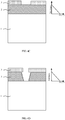
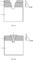
- FIG. 4H shows a schematic structural view of a semiconductor device according to the second embodiment of the present invention.
- a semiconductor device according to the second embodiment is substantially the same as that according to the first embodiment, except that the groove is extended into the semiconductor device active region.
- a method of manufacturing a semiconductor device comprises:
- FIG. 5 shows a schematic view of a semiconductor device according to the third embodiment of the present invention.
- the content of aluminum in the electrode shape controlling layer 2 is gradually reduced from bottom to up, and the reduction is accelerating reduction.
- the other aspects of this embodiments are the same as those of the first embodiment and repeated description will be omitted herein.
- the content of aluminum in the electrode shape controlling layer 2 is gradually reduced from bottom to up, and the reduction is accelerating reduction.
- Sides of the groove are convex slopes protruded toward a central line of the groove.
- the electrode After deposition of the electrode, the electrode has a cross-sectional shape matching the sides of the groove, so that the electric field distribution at the edges of the electrode is changed and the electric field distribution becomes gentle.
- FIG. 6 shows a schematic view of a semiconductor device according to the fourth embodiment of the present invention.
- the content of aluminum in the electrode shape controlling layer 2 is gradually reduced from bottom to up, and the reduction is decelerating reduction.
- the other aspects of this embodiment are the same as those of the first embodiment and repeated description will be omitted herein.
- the content of aluminum in the electrode shape controlling layer 2 is gradually reduced from bottom to up, and the reduction is decelerating reduction.
- Sides of the groove are concave slopes protruded away from a central line of the groove, and the etching cross-section has a U shape.
- the electrode After deposition of the electrode, the electrode has a cross-sectional shape of U shape, so that the electric field distribution at the edges of the electrode is changed and the electric field distribution becomes gentle.
- FIG. 7 shows a schematic view of a semiconductor device according to the fifth embodiment of the present invention.
- the content of aluminum in the electrode shape controlling layer 2 is linearly reduced firstly and then maintains unchanged from bottom to up.
- the other aspects of this embodiment are the same as those of the first embodiment and repeated description will be omitted herein.
- the content of aluminum in the electrode shape controlling layer 2 is linearly reduced firstly and then maintains unchanged.
- the groove includes two parts, the lower part thereof has a shape of trapezoid and the upper part thereof has a shape of rectangle.
- the etching cross-section has the same shape as that of the groove. After deposition of the electrode, the electrode has a cross-section shape the same as that of the etching cross-section.
- FIG. 8 shows a schematic view of a semiconductor device according to the sixth embodiment of the present invention.
- the content of aluminum in the electrode shape controlling layer 2 is decreasingly reduced firstly and then maintains unchanged from bottom to up.
- the other aspects of this embodiment are the same as those of the first embodiment and repeated description will be omitted herein.
- the content of aluminum in the electrode shape controlling layer 2 is decreasingly reduced firstly and then maintains unchanged.
- the groove includes two parts, the lower part thereof has a U shape and the upper part thereof has a shape of rectangle.
- the etching cross-section has the same shape as that of the groove. After deposition of the electrode, the electrode has a cross-section shape the same as that of the etching cross-section.
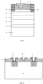
- FIG. 9 shows a schematic view of a semiconductor device according to the seventh embodiment of the present invention.
- a semiconductor device active region is a nitride high electron mobility transistor, comprising a nucleation layer 12 grown on a substrate 11 which can be any type, a nitride buffer layer 13 grown on the nucleation layer 12, a nitride channel layer 14 grown on the nitride buffer layer 13, a nitride barrier layer 15 grown on the nitride channel layer 14, and a nitride capping layer 16 grown on the nitride barrier layer 15.
- An electrode 51 is a gate electrode, an electrode 52 and an electrode 53 are an ohmic contacting source electrode and an ohomic contacting drain electrode respectively.
- the content of aluminum in the electrode shape controlling layer 2 is gradually reduced from bottom to up, and the reduction is accelerating reduction.
- a part of the electrode 51 which is located inside the electrode shape controlling layer 2 has a shape of convex slopes.
- FIG. 10 shows a schematic view of a semiconductor device according to the eighth embodiment of the present invention.
- the semiconductor device active region is an N-channel enhancement mode MOSFET including two highly doped N+ regions 12 and 13 on a P-type substrate 11.
- the electrode shape controlling layer 2 is a dielectric layer in which the content of aluminum is gradually reduced from bottom to up, and the reduction is linear reduction.
- An electrode 51 is a gate electrode
- an electrode 52 is a source electrode
- an electrode 53 is a drain electrode.
- FIG. 11 shows a schematic view of a semiconductor device according to the ninth embodiment of the present invention.
- the semiconductor device active region is a Schottky diode manufactured with a common CMOS process, including an N-type layer 12 on a P-type substrate 11 and an N+ cathode layer 13 on the N-type layer 12.
- the electrode shape controlling layer 2 is a dielectric layer in which the content of aluminum is gradually reduced from bottom to up, and the reduction is linear reduction.
- An electrode 51 is an anode electrode and an electrode 52 is a cathode electrode.
- FIG. 12 shows a schematic view of a semiconductor device according to the tenth embodiment of the present invention.
- the semiconductor device active region is a PN diode having a vertical structure, including a semiconductor N+ layer 12 on a substrate 11, a semiconductor I layer 13 on the semiconductor N+ layer 12, and a semiconductor P+ layer 14 on the semiconductor I layer 13.
- the electrode shape controlling layer 2 is a dielectric layer in which the content of aluminum is gradually reduced from bottom to up, and the reduction is linear reduction.
- An electrode 51 is an anode electrode and an electrode 52 is a cathode electrode.
- an electrode shape controlling layer is added on the semiconductor device active region, and the content of aluminum in the electrode shape controlling layer varies based on change of thickness.
- the ratio of the horizontal etching speed to the vertically etching speed is controlled in the etching process, so that the etching cross-sectional shape is changed in the etching process.
- etching speed is controlled by the material, there is no need to change the process parameters in the etching process, so good controllability, repeatability and simplicity can be realized.
- some particular shapes which cannot be realized with current etching processes can be realized with this invention. By controlling the shapes of the electrodes, distribution of electric field intensity near the electrodes is changed, therefore performances of the semiconductor device, such as breakdown voltage and reliability, are improved.
Landscapes
- Electrodes Of Semiconductors (AREA)
- Insulated Gate Type Field-Effect Transistor (AREA)
- Junction Field-Effect Transistors (AREA)
- Internal Circuitry In Semiconductor Integrated Circuit Devices (AREA)
- Engineering & Computer Science (AREA)
- Manufacturing & Machinery (AREA)
Claims (14)
- Halbleitervorrichtung, welche einen aktiven Halbleiterbereich (1) aufweist, wobei die Halbleitervorrichtung ferner aufweist:eine Elektrodenformsteuerschicht (2), die auf dem aktiven Halbleiterbereich (1) angeordnet ist, wobei die Elektrodenformsteuerschicht (2) Aluminium enthält, wobei der Anteil an Aluminium in der gesamten oder einem Teil der Elektrodenformsteuerschicht (2) in einer Richtung von unten nach oben von dem aktiven Halbleiterbereich (1) verringert ist,einen Elektrodenbereicht, der auf der Elektrodenformsteuerschicht angeordnet ist, wobei der Elektrodenbereicht eine Rille aufweist, die sich in Richtung auf den aktiven Halbleiterbereich (1) erstreckt und die die Elektrodenformsteuerschicht (2) in Längsrichtung durchdringt, wobei alle Teile oder ein Teil einer seitlichen Oberfläche der Rille eine Form einer geraden Neigung, einer konkaven Neigung, die von einer Mittellinie der Rille vorsteht, und einer konvexen Neigung aufweist, die zu der Mittellinie der Rille vorsteht, undeine Elektrode (5), die vollständig oder teilweise in der Rille in dem Elektrodenbereich angeordnet ist, wobei die Elektrode (5) eine Form aufweist, die mit der Form der Rille übereinstimmt, wobei ein Bodenteil der Elektrode mit dem aktiven Bereich der Halbleitervorrichtung (1) kontaktiert ist,wobei die Elektrodenformsteuerschicht (2) eine erste dielektrische Schicht oder eine Kombination der ersten dielektrischen Schicht und einer Halbleiterschicht ist, dadurch gekennzeichnet, dass die erste dielektrische Schicht aus einem von einem SiAlN, einem SiAlOx, einem AlMgON und einem HfAlOx oder einer Kombination davon gebildet worden ist.
- Halbleitervorrichtung nach Anspruch 1, dadurch gekennzeichnet, dass die Elektrodenformsteuerschicht (2) eine Kombination aus einer Halbleiterschicht und einer ersten dielektrischen Schicht ist, wobei die erste dielektrische Schicht über der Halbleiterschicht liegt, deren Anteil an Aluminium an jeder Position der Halbleiterschicht größer als diejenige an einer beliebigen Position der ersten dielektrischen Schicht ist.
- Halbleitervorrichtung nach Anspruch 1 oder Anspruch 2, dadurch gekennzeichnet, dass eine Halbleiterschicht in dem aktiven Halbleiterbereich (1) und die Halbleiterschicht in der Elektrodenformsteuerschicht (2) aus einem von einem Gruppe-III-Nitrid, einem Silicium, einem Germanium, einem Siliciumgermanium, einer III-IV-Verbindung und einem Oxid davon oder einer Kombination davon gebildet worden sind.
- Halbleitervorrichtung nach Anspruch 1, dadurch gekennzeichnet, dass der Anteil an Aluminium auf allen Teilen oder auf einem Teil der Elektrodenformsteuerschicht (2) in der Richtung von unten nach oben von dem aktiven Halbleiterbereich (1) auf eine Art und Weise verringert ist, die eine lineare Verringerung, eine beschleunigende Verringerung, eine verlangsamende Verringerung, eine anfängliche lineare Verringerung und dann eine unverändert bleibende Verringerung, eine anfänglich verlangsamende Verringerung und dann eine unverändert bleibende Verringerung, und eine anfängliche beschleunigende Verringerung und dann eine unverändert bleibende Verringerung ist.
- Halbleitervorrichtung nach Anspruch 1, dadurch gekennzeichnet, dass sich die Rille in der Elektrodenformsteuerschicht (2) in den aktiven Bereich (1) der Halbleitervorrichtung erstreckt.
- Halbleitervorrichtung nach Anspruch 1, dadurch gekennzeichnet, dass eine zweite dielektrische Schicht auf allen Teilen oder auf einem Teil der inneren Wände der Rille in der Elektrodenformsteuerschicht (2) und auf einer Oberfläche der Elektrodenformsteuerschicht (2) abgeschieden worden ist, wobei die Elektrode (5) ganz oder teilweise auf der zweiten dielektrischen Schicht angeordnet ist, und wobei die zweite dielektrische Schicht aus einem Al2O3, einem AION, einem SiN, einem SiON, einem SiO2, einem HfAlOx, einem HfO2 oder einer Kombination davon gebildet worden ist.
- Halbleitervorrichtung nach Anspruch 1, dadurch gekennzeichnet, dass die Halbleitervorrichtung eine Diode ist, wobei die Elektrode (5) eine Anodenelektrode oder eine Kathodenelektrode der Diode ist, oder dass
das Halbleiterbauelement ein Transistor ist und die Elektrode (5) entweder eine Source-Elektrode, eine Drain-Elektrode oder eine Gate-Elektrode des Transistors ist. - Verfahren zur Herstellung einer Halbleitervorrichtung, welches aufweist:S1: ein Bereitstellen eines aktiven Bereichs (1) für eine Halbleitervorrichtung, wobei das Verfahren ferner aufweist:S2: ein Bilden einer Elektrodenformsteuerschicht (2) auf dem aktiven Halbleiterbereich (1), wobei die Elektrodenformsteuerschicht (2) Aluminium enthält, wobei der Anteil an Aluminium in allen Teilen oder in einem Teil der Elektrodenformsteuerschicht (2) in einer Richtung von unten nach oben von dem aktiven Halbleiterbereich (1) verringert ist, wobei die Elektrodenformsteuerschicht (2) eine erste dielektrische Schicht oder eine Kombination der ersten dielektrischen Schicht und einer Halbleiterschicht ist, wobei die erste dielektrische Schicht aus einem SiAlN, einem SiAlOx, einem AlMgON und einem HfAlOx oder einer Kombination davon gebildet worden ist,S3: ein Anordnen eines Elektrodenbereichs auf der Elektrodenformsteuerschicht (2), ein Bilden einer Rille, die sich in Richtung auf den aktiven Bereich (1) der Halbleitervorrichtung erstreckt und die Elektrodenformsteuerschicht (2) in Längsrichtung in dem Elektrodenbereich durchdringt, wobei alle Teile oder ein Teil einer seitlichen Oberfläche der Rille eine Form einer geraden Neigung, einer konkaven Neigung, die von einer Mittellinie der Rille vorsteht, und einer konvexen Neigung aufweist, die zu der Mittellinie der Rille vorsteht, undS4: ein Bilden einer Elektrode in der Rille in dem Elektrodenbereich, wobei die Elektrode (5) ganz oder teilweise in der Rille in dem Elektrodenbereich angeordnet ist, wobei die Elektrode eine Form aufweist, die mit der Form der Rille übereinstimmt, wobei ein Bodenteil der Elektrode mit dem aktiven Bereich des Halbleiterbauelements kontaktiert ist.
- Verfahren zur Herstellung einer Halbleitervorrichtung nach Anspruch 8, dadurch gekennzeichnet, dass die Schritte S3 und S4 aufweisen:S31: ein Aufbringen einer ersten Maskenschicht auf die Elektrodenformsteuerschicht (2) und ein Belichten des Elektrodenbereichs (1) durch eine Photolithographie,S32: ein Ätzen des Elektrodenbereichs, um die Rille zu bilden, die sich zu dem aktiven Halbleiterbereich (1) erstreckt,S33: ein Entfernen der ersten Maskenschicht;S41: ein Aufbringen einer zweiten Maskenschicht auf die Elektrodenformsteuerschicht (2) und ein Belichten des Elektrodenbereichs (1) durch eine Photolithographie, undS42: ein Abscheiden der Elektrode (5) und ein Entfernen der zweiten Maskenschicht, um die Elektrode (5) zu bilden.
- Verfahren zur Herstellung einer Halbleitervorrichtung nach Anspruch 8, dadurch gekennzeichnet, dass die erste dielektrische Schicht mit einem von einer MOCVD, einer PECVD, einer LPCVD, einer MBE, einer CVD und einer GCIB gezüchtet wird.
- Verfahren zur Herstellung einer Halbleitervorrichtung nach Anspruch 8, dadurch gekennzeichnet, dass die Elektrodenformsteuerschicht (2) eine Kombination aus einer Halbleiterschicht und einer ersten dielektrischen Schicht ist, wobei die erste dielektrische Schicht über der Halbleiterschicht angeordnet ist, wobei der Anteil an Aluminium an jeder Position der Halbleiterschicht größer als an einer beliebigen Position der ersten dielektrischen Schicht ist und wobei die erste dielektrische Schicht mit einem von einer MOCVD, einer PECVD, einer LPCVD, einer MBE, einer CVD und einer GCIB gezüchtet wird.
- Verfahren zur Herstellung einer Halbleitervorrichtung nach Anspruch 8, dadurch gekennzeichnet, dass das Verfahren vor dem Schritt S4 weiterhin aufweist:
ein Abscheiden einer zweiten dielektrischen Schicht auf allen Teilen oder auf einem Teil der inneren Wände der Rille in der Elektrodenformsteuerschicht (2) und auf einer Oberfläche der Elektrodenformsteuerschicht (2), wobei die zweite dielektrische Schicht aus einem von einem Al2O3, einem AION, einem SiN, einem SiON, einem SiO2, einem HfAlOx, einem HfO2 oder einer Kombination davon gebildet worden ist. - Verfahren zur Herstellung einer Halbleitervorrichtung nach Anspruch 8, dadurch gekennzeichnet, dass der Anteil an Aluminium in allen Teilen oder in einem Teil der Elektrodenformsteuerschicht (2) in der Richtung von unten nach oben von der aktiven Halbleiterregion (1) auf eine Art und Weise verringert wird, die eine lineare Verringerung, eine beschleunigende Verringerung, eine verlangsamende Verringerung, eine anfängliche lineare Verringerung und dann eine unverändert bleibende Verringerung, eine anfänglich verlangsamende Verringerung und dann eine unverändert bleibende Verringerung, und eine anfängliche beschleunigende Verringerung und dann eine unverändert bleibende Verringerung ist.
- Verfahren zur Herstellung einer Halbleitervorrichtung nach Anspruch 8, dadurch gekennzeichnet, dass sich die Rille in der Elektrodenformsteuerschicht (2) in den aktiven Bereich (1) der Halbleitervorrichtung erstreckt.
Applications Claiming Priority (2)
| Application Number | Priority Date | Filing Date | Title |
|---|---|---|---|
| CN201310223571.7A CN103311284B (zh) | 2013-06-06 | 2013-06-06 | 半导体器件及其制作方法 |
| PCT/CN2014/070150 WO2014194669A1 (zh) | 2013-06-06 | 2014-01-06 | 半导体器件及其制作方法 |
Publications (3)
| Publication Number | Publication Date |
|---|---|
| EP3010043A1 EP3010043A1 (de) | 2016-04-20 |
| EP3010043A4 EP3010043A4 (de) | 2017-03-08 |
| EP3010043B1 true EP3010043B1 (de) | 2019-03-06 |
Family
ID=49136305
Family Applications (1)
| Application Number | Title | Priority Date | Filing Date |
|---|---|---|---|
| EP14807330.7A Active EP3010043B1 (de) | 2013-06-06 | 2014-01-06 | Halbleiterbauelement und herstellungsverfahren dafür |
Country Status (8)
| Country | Link |
|---|---|
| US (1) | US9640624B2 (de) |
| EP (1) | EP3010043B1 (de) |
| JP (1) | JP6195979B2 (de) |
| KR (1) | KR101780890B1 (de) |
| CN (1) | CN103311284B (de) |
| DK (1) | DK3010043T3 (de) |
| SG (1) | SG11201510008UA (de) |
| WO (1) | WO2014194669A1 (de) |
Families Citing this family (11)
| Publication number | Priority date | Publication date | Assignee | Title |
|---|---|---|---|---|
| CN103311284B (zh) * | 2013-06-06 | 2015-11-25 | 苏州晶湛半导体有限公司 | 半导体器件及其制作方法 |
| US9824990B2 (en) | 2014-06-12 | 2017-11-21 | Taiwan Semiconductor Manufacturing Company, Ltd. | Pad design for reliability enhancement in packages |
| US9881857B2 (en) | 2014-06-12 | 2018-01-30 | Taiwan Semiconductor Manufacturing Company, Ltd. | Pad design for reliability enhancement in packages |
| US9812562B1 (en) * | 2016-06-03 | 2017-11-07 | Taiwan Semiconductor Manufacturing Company Ltd. | Semiconductor structure, HEMT structure and method of forming the same |
| JP2018157141A (ja) * | 2017-03-21 | 2018-10-04 | 株式会社東芝 | 半導体装置及び半導体装置の製造方法 |
| CN109935630B (zh) * | 2017-12-15 | 2021-04-23 | 苏州能讯高能半导体有限公司 | 半导体器件及其制造方法 |
| CN112349773A (zh) * | 2019-08-07 | 2021-02-09 | 苏州能讯高能半导体有限公司 | 一种半导体器件及其制备方法 |
| US11424356B2 (en) * | 2020-03-16 | 2022-08-23 | Raytheon Company | Transistor having resistive field plate |
| CN111952360B (zh) * | 2020-08-19 | 2023-02-21 | 深圳方正微电子有限公司 | 场效应管及其制备方法 |
| CN114551340B (zh) * | 2022-01-14 | 2025-06-13 | 深圳镓芯半导体科技有限公司 | 第三代半导体接触窗结构及其制造方法 |
| CN114725194B (zh) * | 2022-02-17 | 2025-07-11 | 西安电子科技大学 | 一种基于栅下场调制的低压终端器件及其制备方法 |
Family Cites Families (19)
| Publication number | Priority date | Publication date | Assignee | Title |
|---|---|---|---|---|
| US6235639B1 (en) | 1998-11-25 | 2001-05-22 | Micron Technology, Inc. | Method of making straight wall containers and the resultant containers |
| KR100403454B1 (ko) * | 2000-06-20 | 2003-11-01 | 주식회사 하이닉스반도체 | 반도체 소자의 금속 배선 형성 방법 |
| KR20020002700A (ko) * | 2000-06-30 | 2002-01-10 | 박종섭 | 금속 배선 형성 방법 |
| US7238560B2 (en) * | 2004-07-23 | 2007-07-03 | Cree, Inc. | Methods of fabricating nitride-based transistors with a cap layer and a recessed gate |
| US7456443B2 (en) | 2004-11-23 | 2008-11-25 | Cree, Inc. | Transistors having buried n-type and p-type regions beneath the source region |
| US7749911B2 (en) * | 2004-11-30 | 2010-07-06 | Taiwan Semiconductor Manufacturing Co., Ltd. | Method for forming an improved T-shaped gate structure |
| US7141486B1 (en) | 2005-06-15 | 2006-11-28 | Agere Systems Inc. | Shallow trench isolation structures comprising a graded doped sacrificial silicon dioxide material and a method for forming shallow trench isolation structures |
| JP2007165446A (ja) * | 2005-12-12 | 2007-06-28 | Oki Electric Ind Co Ltd | 半導体素子のオーミックコンタクト構造 |
| CN101162695A (zh) | 2006-10-09 | 2008-04-16 | 西安能讯微电子有限公司 | 氮化镓hemt器件表面钝化及提高器件击穿电压的工艺 |
| CN101312207B (zh) | 2007-05-21 | 2011-01-05 | 西安捷威半导体有限公司 | 增强型hemt器件及其制造方法 |
| CN101320750A (zh) | 2007-06-06 | 2008-12-10 | 西安能讯微电子有限公司 | Hemt器件及其制造方法 |
| JP2008306083A (ja) * | 2007-06-11 | 2008-12-18 | Nec Corp | Iii−v族窒化物半導体電界効果型トランジスタおよびその製造方法 |
| US7859021B2 (en) * | 2007-08-29 | 2010-12-28 | Sanken Electric Co., Ltd. | Field-effect semiconductor device |
| CN101604704B (zh) * | 2008-06-13 | 2012-09-05 | 西安能讯微电子有限公司 | Hemt器件及其制造方法 |
| JP2010067690A (ja) * | 2008-09-09 | 2010-03-25 | Toshiba Corp | 化合物半導体装置およびその製造方法 |
| JP5496635B2 (ja) * | 2008-12-19 | 2014-05-21 | 住友電工デバイス・イノベーション株式会社 | 半導体装置の製造方法 |
| CN102130158B (zh) * | 2011-01-05 | 2012-07-25 | 西安电子科技大学 | 阶梯型凹槽栅高电子迁移率晶体管 |
| US8716141B2 (en) * | 2011-03-04 | 2014-05-06 | Transphorm Inc. | Electrode configurations for semiconductor devices |
| CN103311284B (zh) * | 2013-06-06 | 2015-11-25 | 苏州晶湛半导体有限公司 | 半导体器件及其制作方法 |
-
2013
- 2013-06-06 CN CN201310223571.7A patent/CN103311284B/zh active Active
-
2014
- 2014-01-06 SG SG11201510008UA patent/SG11201510008UA/en unknown
- 2014-01-06 US US14/896,364 patent/US9640624B2/en active Active
- 2014-01-06 EP EP14807330.7A patent/EP3010043B1/de active Active
- 2014-01-06 KR KR1020157037194A patent/KR101780890B1/ko active Active
- 2014-01-06 JP JP2016517130A patent/JP6195979B2/ja active Active
- 2014-01-06 DK DK14807330.7T patent/DK3010043T3/da active
- 2014-01-06 WO PCT/CN2014/070150 patent/WO2014194669A1/zh not_active Ceased
Non-Patent Citations (1)
| Title |
|---|
| None * |
Also Published As
| Publication number | Publication date |
|---|---|
| CN103311284A (zh) | 2013-09-18 |
| JP6195979B2 (ja) | 2017-09-13 |
| EP3010043A1 (de) | 2016-04-20 |
| US20160126325A1 (en) | 2016-05-05 |
| SG11201510008UA (en) | 2016-01-28 |
| WO2014194669A1 (zh) | 2014-12-11 |
| DK3010043T3 (da) | 2019-05-06 |
| KR101780890B1 (ko) | 2017-09-21 |
| JP2016524817A (ja) | 2016-08-18 |
| US9640624B2 (en) | 2017-05-02 |
| KR20160013218A (ko) | 2016-02-03 |
| CN103311284B (zh) | 2015-11-25 |
| EP3010043A4 (de) | 2017-03-08 |
Similar Documents
| Publication | Publication Date | Title |
|---|---|---|
| EP3010043B1 (de) | Halbleiterbauelement und herstellungsverfahren dafür | |
| US10964806B2 (en) | Gallium nitride transistor | |
| US9419121B1 (en) | Semiconductor device with multiple carrier channels | |
| US9293538B2 (en) | Diode having trenches in a semiconductor region | |
| US10283591B2 (en) | Silicon carbide semiconductor device and method of manufacturing the silicon carbide semiconductor device | |
| CN101930999B (zh) | 具有非晶沟道控制层的半导体部件 | |
| EP2992559A1 (de) | Resurf-iii-n-transistor mit hoher elektronenmobilität | |
| TW201914026A (zh) | 氮化物半導體元件 | |
| US12268018B2 (en) | GaN vertical trench MOSFETs and methods of manufacturing the same | |
| WO2015175915A1 (en) | Trenched vertical power field-effect transistors with improved on-resistance and breakdown voltage | |
| CN102881716A (zh) | 一种场致隧穿增强型hemt器件 | |
| US20200220000A1 (en) | GaN-Based HEMT Device | |
| US10026835B2 (en) | Field boosted metal-oxide-semiconductor field effect transistor | |
| KR102067596B1 (ko) | 질화물 반도체 소자 및 그 제조 방법 | |
| TWI817719B (zh) | 半導體結構及其形成方法 | |
| US9450085B2 (en) | Semiconductor device and method for producing a semiconductor device | |
| CN114649410A (zh) | 沟槽型半导体器件及其制造方法 | |
| JP2014154609A (ja) | 半導体装置 | |
| US20240395923A1 (en) | Semiconductor device and method of manufacturing the same | |
| US12615830B2 (en) | Semiconductor structure and method for forming the same | |
| US20260059791A1 (en) | Mosfet device based on nio gate modulation and its preparation method | |
| US20240170544A1 (en) | Semiconductor structure and method for forming the same | |
| KR101622916B1 (ko) | 양성자 빔 조사에 의한 상시불통형 GaN계 트랜지스터 및 그 제조 방법 |
Legal Events
| Date | Code | Title | Description |
|---|---|---|---|
| PUAI | Public reference made under article 153(3) epc to a published international application that has entered the european phase |
Free format text: ORIGINAL CODE: 0009012 |
|
| 17P | Request for examination filed |
Effective date: 20151228 |
|
| AK | Designated contracting states |
Kind code of ref document: A1 Designated state(s): AL AT BE BG CH CY CZ DE DK EE ES FI FR GB GR HR HU IE IS IT LI LT LU LV MC MK MT NL NO PL PT RO RS SE SI SK SM TR |
|
| AX | Request for extension of the european patent |
Extension state: BA ME |
|
| RIN1 | Information on inventor provided before grant (corrected) |
Inventor name: CHENG, KAI |
|
| DAX | Request for extension of the european patent (deleted) | ||
| A4 | Supplementary search report drawn up and despatched |
Effective date: 20170206 |
|
| RIC1 | Information provided on ipc code assigned before grant |
Ipc: H01L 29/43 20060101AFI20170131BHEP Ipc: H01L 29/49 20060101ALI20170131BHEP Ipc: H01L 21/28 20060101ALI20170131BHEP |
|
| STAA | Information on the status of an ep patent application or granted ep patent |
Free format text: STATUS: EXAMINATION IS IN PROGRESS |
|
| 17Q | First examination report despatched |
Effective date: 20180221 |
|
| RIC1 | Information provided on ipc code assigned before grant |
Ipc: H01L 29/868 20060101ALI20180802BHEP Ipc: H01L 29/423 20060101ALI20180802BHEP Ipc: H01L 29/778 20060101ALI20180802BHEP Ipc: H01L 29/49 20060101ALI20180802BHEP Ipc: H01L 29/417 20060101ALI20180802BHEP Ipc: H01L 29/41 20060101AFI20180802BHEP Ipc: H01L 29/872 20060101ALI20180802BHEP Ipc: H01L 21/768 20060101ALN20180802BHEP |
|
| REG | Reference to a national code |
Ref country code: DE Ref legal event code: R079 Ref document number: 602014042476 Country of ref document: DE Free format text: PREVIOUS MAIN CLASS: H01L0029430000 Ipc: H01L0029410000 |
|
| GRAP | Despatch of communication of intention to grant a patent |
Free format text: ORIGINAL CODE: EPIDOSNIGR1 |
|
| STAA | Information on the status of an ep patent application or granted ep patent |
Free format text: STATUS: GRANT OF PATENT IS INTENDED |
|
| RIC1 | Information provided on ipc code assigned before grant |
Ipc: H01L 29/417 20060101ALI20180912BHEP Ipc: H01L 21/768 20060101ALN20180912BHEP Ipc: H01L 29/49 20060101ALI20180912BHEP Ipc: H01L 29/778 20060101ALI20180912BHEP Ipc: H01L 29/41 20060101AFI20180912BHEP Ipc: H01L 29/423 20060101ALI20180912BHEP Ipc: H01L 29/868 20060101ALI20180912BHEP Ipc: H01L 29/872 20060101ALI20180912BHEP |
|
| INTG | Intention to grant announced |
Effective date: 20180925 |
|
| GRAS | Grant fee paid |
Free format text: ORIGINAL CODE: EPIDOSNIGR3 |
|
| GRAA | (expected) grant |
Free format text: ORIGINAL CODE: 0009210 |
|
| STAA | Information on the status of an ep patent application or granted ep patent |
Free format text: STATUS: THE PATENT HAS BEEN GRANTED |
|
| RAP1 | Party data changed (applicant data changed or rights of an application transferred) |
Owner name: ENKRIS SEMICONDUCTOR, INC. |
|
| AK | Designated contracting states |
Kind code of ref document: B1 Designated state(s): AL AT BE BG CH CY CZ DE DK EE ES FI FR GB GR HR HU IE IS IT LI LT LU LV MC MK MT NL NO PL PT RO RS SE SI SK SM TR |
|
| REG | Reference to a national code |
Ref country code: GB Ref legal event code: FG4D |
|
| REG | Reference to a national code |
Ref country code: CH Ref legal event code: EP Ref country code: AT Ref legal event code: REF Ref document number: 1105705 Country of ref document: AT Kind code of ref document: T Effective date: 20190315 |
|
| REG | Reference to a national code |
Ref country code: DE Ref legal event code: R096 Ref document number: 602014042476 Country of ref document: DE |
|
| REG | Reference to a national code |
Ref country code: IE Ref legal event code: FG4D |
|
| REG | Reference to a national code |
Ref country code: DK Ref legal event code: T3 Effective date: 20190429 |
|
| REG | Reference to a national code |
Ref country code: NL Ref legal event code: MP Effective date: 20190306 |
|
| REG | Reference to a national code |
Ref country code: LT Ref legal event code: MG4D |
|
| PG25 | Lapsed in a contracting state [announced via postgrant information from national office to epo] |
Ref country code: LT Free format text: LAPSE BECAUSE OF FAILURE TO SUBMIT A TRANSLATION OF THE DESCRIPTION OR TO PAY THE FEE WITHIN THE PRESCRIBED TIME-LIMIT Effective date: 20190306 Ref country code: SE Free format text: LAPSE BECAUSE OF FAILURE TO SUBMIT A TRANSLATION OF THE DESCRIPTION OR TO PAY THE FEE WITHIN THE PRESCRIBED TIME-LIMIT Effective date: 20190306 Ref country code: NO Free format text: LAPSE BECAUSE OF FAILURE TO SUBMIT A TRANSLATION OF THE DESCRIPTION OR TO PAY THE FEE WITHIN THE PRESCRIBED TIME-LIMIT Effective date: 20190606 Ref country code: FI Free format text: LAPSE BECAUSE OF FAILURE TO SUBMIT A TRANSLATION OF THE DESCRIPTION OR TO PAY THE FEE WITHIN THE PRESCRIBED TIME-LIMIT Effective date: 20190306 |
|
| PG25 | Lapsed in a contracting state [announced via postgrant information from national office to epo] |
Ref country code: HR Free format text: LAPSE BECAUSE OF FAILURE TO SUBMIT A TRANSLATION OF THE DESCRIPTION OR TO PAY THE FEE WITHIN THE PRESCRIBED TIME-LIMIT Effective date: 20190306 Ref country code: NL Free format text: LAPSE BECAUSE OF FAILURE TO SUBMIT A TRANSLATION OF THE DESCRIPTION OR TO PAY THE FEE WITHIN THE PRESCRIBED TIME-LIMIT Effective date: 20190306 Ref country code: GR Free format text: LAPSE BECAUSE OF FAILURE TO SUBMIT A TRANSLATION OF THE DESCRIPTION OR TO PAY THE FEE WITHIN THE PRESCRIBED TIME-LIMIT Effective date: 20190607 Ref country code: LV Free format text: LAPSE BECAUSE OF FAILURE TO SUBMIT A TRANSLATION OF THE DESCRIPTION OR TO PAY THE FEE WITHIN THE PRESCRIBED TIME-LIMIT Effective date: 20190306 Ref country code: BG Free format text: LAPSE BECAUSE OF FAILURE TO SUBMIT A TRANSLATION OF THE DESCRIPTION OR TO PAY THE FEE WITHIN THE PRESCRIBED TIME-LIMIT Effective date: 20190606 Ref country code: RS Free format text: LAPSE BECAUSE OF FAILURE TO SUBMIT A TRANSLATION OF THE DESCRIPTION OR TO PAY THE FEE WITHIN THE PRESCRIBED TIME-LIMIT Effective date: 20190306 |
|
| REG | Reference to a national code |
Ref country code: AT Ref legal event code: MK05 Ref document number: 1105705 Country of ref document: AT Kind code of ref document: T Effective date: 20190306 |
|
| PG25 | Lapsed in a contracting state [announced via postgrant information from national office to epo] |
Ref country code: PT Free format text: LAPSE BECAUSE OF FAILURE TO SUBMIT A TRANSLATION OF THE DESCRIPTION OR TO PAY THE FEE WITHIN THE PRESCRIBED TIME-LIMIT Effective date: 20190706 Ref country code: SK Free format text: LAPSE BECAUSE OF FAILURE TO SUBMIT A TRANSLATION OF THE DESCRIPTION OR TO PAY THE FEE WITHIN THE PRESCRIBED TIME-LIMIT Effective date: 20190306 Ref country code: AL Free format text: LAPSE BECAUSE OF FAILURE TO SUBMIT A TRANSLATION OF THE DESCRIPTION OR TO PAY THE FEE WITHIN THE PRESCRIBED TIME-LIMIT Effective date: 20190306 Ref country code: ES Free format text: LAPSE BECAUSE OF FAILURE TO SUBMIT A TRANSLATION OF THE DESCRIPTION OR TO PAY THE FEE WITHIN THE PRESCRIBED TIME-LIMIT Effective date: 20190306 Ref country code: CZ Free format text: LAPSE BECAUSE OF FAILURE TO SUBMIT A TRANSLATION OF THE DESCRIPTION OR TO PAY THE FEE WITHIN THE PRESCRIBED TIME-LIMIT Effective date: 20190306 Ref country code: RO Free format text: LAPSE BECAUSE OF FAILURE TO SUBMIT A TRANSLATION OF THE DESCRIPTION OR TO PAY THE FEE WITHIN THE PRESCRIBED TIME-LIMIT Effective date: 20190306 Ref country code: IT Free format text: LAPSE BECAUSE OF FAILURE TO SUBMIT A TRANSLATION OF THE DESCRIPTION OR TO PAY THE FEE WITHIN THE PRESCRIBED TIME-LIMIT Effective date: 20190306 Ref country code: EE Free format text: LAPSE BECAUSE OF FAILURE TO SUBMIT A TRANSLATION OF THE DESCRIPTION OR TO PAY THE FEE WITHIN THE PRESCRIBED TIME-LIMIT Effective date: 20190306 |
|
| PG25 | Lapsed in a contracting state [announced via postgrant information from national office to epo] |
Ref country code: SM Free format text: LAPSE BECAUSE OF FAILURE TO SUBMIT A TRANSLATION OF THE DESCRIPTION OR TO PAY THE FEE WITHIN THE PRESCRIBED TIME-LIMIT Effective date: 20190306 Ref country code: PL Free format text: LAPSE BECAUSE OF FAILURE TO SUBMIT A TRANSLATION OF THE DESCRIPTION OR TO PAY THE FEE WITHIN THE PRESCRIBED TIME-LIMIT Effective date: 20190306 |
|
| REG | Reference to a national code |
Ref country code: DE Ref legal event code: R097 Ref document number: 602014042476 Country of ref document: DE |
|
| PG25 | Lapsed in a contracting state [announced via postgrant information from national office to epo] |
Ref country code: AT Free format text: LAPSE BECAUSE OF FAILURE TO SUBMIT A TRANSLATION OF THE DESCRIPTION OR TO PAY THE FEE WITHIN THE PRESCRIBED TIME-LIMIT Effective date: 20190306 Ref country code: IS Free format text: LAPSE BECAUSE OF FAILURE TO SUBMIT A TRANSLATION OF THE DESCRIPTION OR TO PAY THE FEE WITHIN THE PRESCRIBED TIME-LIMIT Effective date: 20190706 |
|
| PLBE | No opposition filed within time limit |
Free format text: ORIGINAL CODE: 0009261 |
|
| STAA | Information on the status of an ep patent application or granted ep patent |
Free format text: STATUS: NO OPPOSITION FILED WITHIN TIME LIMIT |
|
| 26N | No opposition filed |
Effective date: 20191209 |
|
| PG25 | Lapsed in a contracting state [announced via postgrant information from national office to epo] |
Ref country code: SI Free format text: LAPSE BECAUSE OF FAILURE TO SUBMIT A TRANSLATION OF THE DESCRIPTION OR TO PAY THE FEE WITHIN THE PRESCRIBED TIME-LIMIT Effective date: 20190306 |
|
| PG25 | Lapsed in a contracting state [announced via postgrant information from national office to epo] |
Ref country code: TR Free format text: LAPSE BECAUSE OF FAILURE TO SUBMIT A TRANSLATION OF THE DESCRIPTION OR TO PAY THE FEE WITHIN THE PRESCRIBED TIME-LIMIT Effective date: 20190306 |
|
| PG25 | Lapsed in a contracting state [announced via postgrant information from national office to epo] |
Ref country code: MC Free format text: LAPSE BECAUSE OF FAILURE TO SUBMIT A TRANSLATION OF THE DESCRIPTION OR TO PAY THE FEE WITHIN THE PRESCRIBED TIME-LIMIT Effective date: 20190306 |
|
| REG | Reference to a national code |
Ref country code: CH Ref legal event code: PL |
|
| PG25 | Lapsed in a contracting state [announced via postgrant information from national office to epo] |
Ref country code: LU Free format text: LAPSE BECAUSE OF NON-PAYMENT OF DUE FEES Effective date: 20200106 |
|
| PG25 | Lapsed in a contracting state [announced via postgrant information from national office to epo] |
Ref country code: CH Free format text: LAPSE BECAUSE OF NON-PAYMENT OF DUE FEES Effective date: 20200131 Ref country code: LI Free format text: LAPSE BECAUSE OF NON-PAYMENT OF DUE FEES Effective date: 20200131 |
|
| PG25 | Lapsed in a contracting state [announced via postgrant information from national office to epo] |
Ref country code: IE Free format text: LAPSE BECAUSE OF NON-PAYMENT OF DUE FEES Effective date: 20200106 |
|
| PG25 | Lapsed in a contracting state [announced via postgrant information from national office to epo] |
Ref country code: MT Free format text: LAPSE BECAUSE OF FAILURE TO SUBMIT A TRANSLATION OF THE DESCRIPTION OR TO PAY THE FEE WITHIN THE PRESCRIBED TIME-LIMIT Effective date: 20190306 Ref country code: CY Free format text: LAPSE BECAUSE OF FAILURE TO SUBMIT A TRANSLATION OF THE DESCRIPTION OR TO PAY THE FEE WITHIN THE PRESCRIBED TIME-LIMIT Effective date: 20190306 |
|
| PG25 | Lapsed in a contracting state [announced via postgrant information from national office to epo] |
Ref country code: MK Free format text: LAPSE BECAUSE OF FAILURE TO SUBMIT A TRANSLATION OF THE DESCRIPTION OR TO PAY THE FEE WITHIN THE PRESCRIBED TIME-LIMIT Effective date: 20190306 |
|
| REG | Reference to a national code |
Ref country code: DE Ref legal event code: R079 Ref document number: 602014042476 Country of ref document: DE Free format text: PREVIOUS MAIN CLASS: H01L0029410000 Ipc: H10D0064200000 |
|
| PGFP | Annual fee paid to national office [announced via postgrant information from national office to epo] |
Ref country code: DK Payment date: 20251230 Year of fee payment: 13 |
|
| PGFP | Annual fee paid to national office [announced via postgrant information from national office to epo] |
Ref country code: GB Payment date: 20260127 Year of fee payment: 13 |
|
| PGFP | Annual fee paid to national office [announced via postgrant information from national office to epo] |
Ref country code: DE Payment date: 20260114 Year of fee payment: 13 |
|
| PGFP | Annual fee paid to national office [announced via postgrant information from national office to epo] |
Ref country code: BE Payment date: 20260119 Year of fee payment: 13 |
|
| PGFP | Annual fee paid to national office [announced via postgrant information from national office to epo] |
Ref country code: FR Payment date: 20260128 Year of fee payment: 13 |