EP3016287B1 - Dispositif de porte majoritaire à couple de spin - Google Patents
Dispositif de porte majoritaire à couple de spin Download PDFInfo
- Publication number
- EP3016287B1 EP3016287B1 EP14192272.4A EP14192272A EP3016287B1 EP 3016287 B1 EP3016287 B1 EP 3016287B1 EP 14192272 A EP14192272 A EP 14192272A EP 3016287 B1 EP3016287 B1 EP 3016287B1
- Authority
- EP
- European Patent Office
- Prior art keywords
- input
- zone
- output
- gate device
- majority gate
- Prior art date
- Legal status (The legal status is an assumption and is not a legal conclusion. Google has not performed a legal analysis and makes no representation as to the accuracy of the status listed.)
- Active
Links
Images








Classifications
-
- H—ELECTRICITY
- H03—ELECTRONIC CIRCUITRY
- H03K—PULSE TECHNIQUE
- H03K19/00—Logic circuits, i.e. having at least two inputs acting on one output; Inverting circuits
- H03K19/20—Logic circuits, i.e. having at least two inputs acting on one output; Inverting circuits characterised by logic function, e.g. AND, OR, NOR, NOT circuits
- H03K19/23—Majority or minority circuits, i.e. giving output having the state of the majority or the minority of the inputs
-
- H—ELECTRICITY
- H03—ELECTRONIC CIRCUITRY
- H03K—PULSE TECHNIQUE
- H03K19/00—Logic circuits, i.e. having at least two inputs acting on one output; Inverting circuits
- H03K19/02—Logic circuits, i.e. having at least two inputs acting on one output; Inverting circuits using specified components
- H03K19/18—Logic circuits, i.e. having at least two inputs acting on one output; Inverting circuits using specified components using galvano-magnetic devices, e.g. Hall-effect devices
-
- H—ELECTRICITY
- H10—SEMICONDUCTOR DEVICES; ELECTRIC SOLID-STATE DEVICES NOT OTHERWISE PROVIDED FOR
- H10N—ELECTRIC SOLID-STATE DEVICES NOT OTHERWISE PROVIDED FOR
- H10N50/00—Galvanomagnetic devices
- H10N50/10—Magnetoresistive devices
Definitions
- the present disclosure generally relates to magnetic devices, more specifically to spin torque majority gate devices.
- CMOS logic circuits One of the issues of current CMOS logic circuits is the increase in power consumption density when scaling down devices.
- One of the main candidates to replace CMOS logic is spintronics where the magnetization is used as the signal instead of the electric charge. Using properties of spintronics, a type of device called "majority gate" can be built.
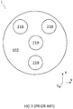
- the spin torque majority gate consists of a common free (switchable) ferromagnetic (FM) layer 202 and thereon four independent fixed FM layers 2181, 2182, 2183, 2191 in each of the nanopillars 218, 219 -three for the inputs 218 and one for the output 219.
- FM ferromagnetic
- the free FM layer 202 and fixed FM layers 2181, 2182, 2183, 2191 are separated by a non-magnetic spacer layer 204.
- the operation of the device is based on spin transfer torque.
- the device operates by applying a positive or negative voltage to each input nanopillar 218, which thereby determines the directions of current flowing through each nanopillar 218 and the resulting spin torques.
- the free FM layer 202 can be in one of the two stable states of magnetization (shown by the arrow 2021, being 'up' in FIG 2 ) corresponding to logical "0" and "1."
- Spin torques act to retain the gate in its state or to switch it to the opposite state, depending on their direction (shown by the arrows, being 'up' for 2181 and 2182 and being 'down' for 2183). The majority of the torques determines the outcome.
- the state of magnetization is detected by magnetoresistance (MR) between the free 202 and the fixed layers 118 by the output pillar 219.
- MR magnetoresistance
- spin torque majority gate (STMG) devices that, in principle, an operation can be realized that would otherwise necessitate at least nineteen transistors in a CMOS circuit.
- Spin-based logic/spintronics could potentially reduce power consumption and be more compact than CMOS circuits. Additionally, part of the logic circuit could be moved to the interconnect level and allow stacking, thus further reducing footprint.
- a spin torque majority gate device allows reducing the complexity at the circuit level by bringing it at the device level in a compact form.
- a majority gate device comprising a free ferromagnetic layer comprising 3N input zones and one polygon output zone having 3N sides, each input zone adjoining the output zone and being positioned around the output zone according to a 3N-fold rotational symmetry with N being an integer larger than 0, whereby the input zones are spaced apart from one another by the output zone; each input zone being magnetically coupled to a corresponding input control, the input control for controlling the magnetization state of the corresponding input zone; and an output sensor magnetically coupled to the output zone, the output sensor for sensing the magnetization state of the output zone.
- Each input zone is thus adjoining the output zone at one of its 3N sides.
- N is preferably chosen from 1, 2, 3 or 4.
- a majority gate with a 3-fold rotational symmetry will thus comprise a triangle output having 3 sides and 3 input zones arranged around and in contact with the output zone.
- a majority gate with a 6-fold rotational symmetry will thus comprise a hexagon output having 6 sides and 6 input zones arranged around and in contact with the output zone.
- the input zones are substantially spaced apart from one another. This means an input zone may intersect with another input zone at one point. This intersecting point is moreover an intersection point with the output zone.
- the input zone may also be spaced apart from another input zone by a certain distance. The distance spacing apart two neighboring input zones is preferably smaller than the width of the domain wall (between the input zones and the output zones).
- the output zone and each input zone correspond to a magnetic domain of the free ferromagnetic material, each magnetic domain having a single or uniform magnetization state.
- Each input zone thus corresponds to a single magnetic domain with a uniform magnetization state.
- the output zone thus corresponds to a single magnetic domain with a uniform magnetization state.
- the magnetization of the free ferromagnetic layer is out-of-plane.
- each input control is magnetically coupled to the corresponding input zone by a magnetic tunnel junction (MTJ).
- MTJ magnetic tunnel junction
- the output sensor may be magnetically coupled to the corresponding output zone by a magnetic tunnel junction (MTJ).
- MTJ magnetic tunnel junction
- the MTJ may be formed by a stack comprising a non-magnetic insulating layer present in between the free ferromagnetic layer and a fixed ferromagnetic layer.
- the input control and/or output sensor may comprise the non-magnetic insulating layer and the fixed ferromagnetic layer.
- the nonmagnetic insulating layer may also be present over the entire surface of the free ferromagnetic layer, not being part of the input control and/or output sensor.
- each input control may be magnetically coupled to the corresponding input zone by Spin Hall Effect.
- the distance between each input control and the output sensor is preferably smaller than 400nm, more preferably smaller than 200nm.
- the input control and/or the output sensor are circular pillars.
- each input zone may be subdivided in neighboring input subzones, the corresponding input control of the input zone being magnetically coupled to one of the input subzones.
- the majority gate device further comprises for each remaining input subzone another corresponding input control, the another input control being magnetically coupled to its corresponding input subzone.
- the input controls of each input subzone are electrically connected.
- the input zone has a shape chosen from an isosceles trapezoid, a rectangle, a square, a triangle, a segment or a semicircle.
- the segment may be a major segment of a circle or a minor segment of a circle.
- the width of the input zone decreases towards the output zone.
- a three dimensional majority gate device comprising a second layer of majority gate devices according to the preferred embodiments stacked on a first layer of majority gate devices according to the preferred embodiments wherein the output zone of a majority gate device of the first layer is coupled to an input zone of a majority gate device of the second layer.
- a method for operating the majority gate device comprising the steps of applying a predetermined voltage to each input control for providing the magnetization state of the output zone; and thereafter, determining the combined effect of the predetermined voltages on the current of the output sensor which is determined by the magnetization state of the output zone.
- the magnetization state of the output zone equals the majority magnetization state of the input zones.
- the combined effect of the predetermined voltages induces the adjoining of at least two domain walls and the propagation of the adjoined domain walls entirely through the output zone.
- the magnetization state of the input zones and/or the output sensor may be controlled and or sensed by in-plane current, Spin Hall Effect, Giant spin Hall effect, Rashba torque, Spin-Orbit torque, magnetic field generated by a current, magnetic field generated by additional ferromagnetic layers (stray field) or Voltage Controlled Anisotropy (electric field).
- the majority gate device can be scaled to a smaller size than the majority gate realized with CMOS transistors.
- the device works for large effective anisotropy i.e. large thermal stability. Therefore, the retention time can be large; a logic device that is non-volatile can be made. This means it does not suffer from standby power dissipation.
- the majority gate device according to the present disclosure is compatible with current lithography processing, wherein the critical dimension can be large while maintaining compactness of the device. This means the manufacturing of the majority gate device according to the present disclosure is not dependent on very advanced lithography processes (such as for example extreme ultraviolet lithography).
- logic circuits may be build. These logic devices can be fabricated in the metal layers (back-end of line/interconnect) and can be combined with logic layer in the front-end (i.e. at transistor level). This has the advantage of allowing for three dimensional stacking of devices.
- first, second and the like in the description are used for distinguishing between similar elements and not necessarily for describing a sequence, either temporally, spatially, in ranking or in any other manner. It is to be understood that the terms so used are interchangeable under appropriate circumstances and that the embodiments of the disclosure described herein are capable of operation in other sequences than described or illustrated herein.
- an object with rotational symmetry also known as radial symmetry
- N-fold rotational symmetry also called rotational symmetry of order n or discrete rotational symmetry of the n th order
- a 3-fold rotational symmetry thus means that the shape remains the same by rotation of 120°.
- the input zones being positioned relative to each other with respect to the output zone according to a 3N-fold rotational symmetry thus means that by rotating the input zones with 120°/N the shape remains unchanged, with N being an integer larger than 0.
- the rotational symmetry with respect to any angle is referred to as circular symmetry.
- a 3N-fold rotational symmetry excludes circular symmetry. N can thus not be infinite.
- a 'domain wall' or 'DW' is an interface separating magnetic domains (see FIG 9 ). It is a transition between different magnetic moments and usually undergoes an angular displacement of 90° or 180°.
- a 'domain wall' or 'DW' is a gradual reorientation of individual moments across a finite distance. The domain wall width depends on the exchange A ex and the effective anisotropy K eff of the material ⁇ A ex K eff , which is about 10 to 50 nm in most cases.
- the critical size depends on the width a of the arms of the crossbar and the material parameters of the ferromagnetic layers such as the effective anisotropy K eff and the exchange stiffness constant A ex .
- the initial state of the crossbar STMG (as in FIG 1 ) is chosen to be an "UP" state (with small deviations possible) as shown in FIG 4A . If at least two of the three inputs induce an 'UP' magnetization state (for example with a positive voltage '+'), then the expected output magnetization should also be 'UP' and thus no switching will occur ( FIG 4B, 4C ). If however at least two of the three inputs induce a 'DOWN' magnetization state (for example with a negative voltage '-'), then the expected output magnetization should become 'DOWN' and thus switching will occur ( FIG 4D, 4E, 4F ).
- W 40nm
- a ex 2e-11J/m
- K eff 110kJ/m 3
- a pulse of 4ns Although two of the input pillars 218 have a negative ('-') magnetization, the output magnetization 219 remains positive. It can be seen that at the center of the cross 800 the domain wall is stuck and did not propagate further towards the output pillar.
- the initial state is UP ; the spin torque reverses the magnetization at the bottom left and the bottom right of the image, while it keeps the magnetization UP at the top of the image.
- the magnetic domain nucleated at the bottom left moves slowly along the edge of the free layer. When it reaches the zone where the spin torque is UP (at the top of the image), it is annihilated.
- FIG 6A-E shows five possible layouts for an STMG device according to embodiments of the present disclosure.
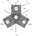
- Each layout comprises three input zones 121, 122, 123 arranged around and in contact with an output zone 124 (thus for 3-fold rotational symmetry, the output zone having 3 sides and each of the input zones in contact with a side of the output zone).
- the input zones 121, 122, 123 are separate from one another but in contact with the output zone 124 by a triangle-shaped boundary.
- Neighboring input zones may intersect with one another at one point of the output zone or may be at a small distance from one another.
- the distance separating neighboring input zone should preferably be smaller than the width of the domain wall formed between the input zone and the output zone.
- Each input zone is coupled to at least one input control 118.
- FIG 6A and FIG 6B are referred to a 'circle segment' layout as the input zones have the shape of a segment of a circle;
- FIG 6C and FIG 6E are referred to a 'triangle' layout as the input zones have the shape of a triangle;
- FIG 6D is referred to a 'square' layout as the input zones have the shape of a square.
- the segment for a 'segment' layout may be a minor segment (such as in FIG 6A ) or a major segment (such as in FIG 6B ).
- the shape of the input zone for a 'segment' layout may also be a semicircle which is a special case of a segment.
- Each input zone and the output zone corresponds to a magnetic domain of the free ferromagnetic material, each magnetic domain having a magnetization state. If two or three input zones have a magnetization being 'UP', then the magnetization of the magnetic domain corresponding to the output zone should be 'UP', being equal to the majority magnetization of the three input zones. If two or three input zones have a magnetization being 'DOWN', then the magnetization of the magnetic domain corresponding to the output zone should be 'DOWN', being equal to the majority magnetization of the three input zones.
- the majority gate device 2 comprises a free ferromagnetic layer 112 on a substrate.
- the free ferromagnetic layer 112 has a shape which has 3-fold rotational symmetry.
- the free ferromagnetic layer 112 comprises three input zones 121, 122, 123 and one triangular output zone 124.
- the output zone has a boundary 130 consisting of three boundary lines 131, 132, 133 with each input zone 121, 122, 123. These four zones 121, 122, 123, 124 have a non-zero magnetization which is out-of-plane at equilibrium.
- each input zone 121, 122, 123 is controlled by at least one input control 1181, 1182, 1183 (e.g. by Spin Transfer Torque (STT)) such that it can be switched to the desired 'UP' or 'DOWN' state, corresponding respectively to the logic states '0' and '1'.
- the magnetization of the output zone 124 may be read by an output sensor 119.
- the output sensor functions thus as a read-out device.
- the input controls 1181, 1182, 1183 are magnetically coupled to each input zone 121, 122, 123 respectively.
- the output sensor 119 is also magnetically coupled to the output zone 124.
- the input zones 121, 122, 123 should be located along three axes 151, 152, 152 forming three angles ⁇ 1, ⁇ 2, ⁇ 3 each (close to) 120 degrees.
- the input zones 121, 122, 123 are thus located according to a 3-fold rotational symmetry.
- the output zone 124 (and as a consequence also the output sensor 119) is preferentially centered at the intersection of these three axes 151, 152, 152.
- the output zone 124 may be slightly off-centered, not more than 50nm, preferably not more than 20nm from the intersection of the three axes 151, 152, 152.
- neighboring input zones 121, 122, 123 intersect each other respectively at one point thereby forming a triangular boundary 130 with the output zone as shown in FIG 7 .
- the neighboring input zones 121, 122, 123 do not need to intersect, but may be separated at a certain distance 200 from one another.
- the neighboring intersection points of the input zones with the output zone should be at a distance 200 from one another which is typically smaller than the width of the domain wall.
- FIG. 8A-B shows simulations representing the spontaneous evolution of the magnetization (and the domain walls 181, 182).
- a triangular boundary between the input zones and the output zone is optimal, because in this case the domain walls between the input zones and the output zone are merging at the intersection point between neighboring input zones.
- the intersection points thus form the vertices of the triangular output zone.
- the domain walls 181, 182 may/can merge and propagate through the output zone, the domain wall 183 ending in its minimum energy, just as in the triangular case.
- the output zone preferably has a triangular shape (i.e. for a 3-fold rotational symmetry) and thus a triangular boundary with the neighboring input zones.
- the cross section is narrowed at the contact area between the output zone and each input zone.
- the output zone should have an equilateral triangular shape, which means the three sides or boundary lines should be equally sized. As a consequence, each vertex of the equilateral triangular output zone is in contact with two input zones.
- FIG 10A shows simulation results for the device in an initial state with the magnetization being 'UP' for one (first 121) input zone and being 'DOWN' for the two remaining (second 122 and third 123) input zone. This means the majority magnetization is 'DOWN'
- the output zone 124 is centered relative to the tree input zones 121, 122, 123.
- a triangular boundary zone 130 (shown with dashed line) may be defined as the boundary region between the input zones 121, 122, 123 and the output zone 124.
- the triangular boundary zone 130 consists of three boundary lines 131, 132, 133 and three intersection points 134, 135, 136.
- FIG 10B shows simulations for the device during a pulse applied to the input controls (or directly after the pulse).
- Domain walls 182,183 are formed at the boundary lines 132 and 133, however at the intersection point 136 between the two boundary lines, the domain walls 182, 183, join to form one large (angulated) domain wall 181 which is however unstable and will try to propagate further towards its minimal energy resulting in FIG10C.
- FIG 10C illustrates simulation results of the magnetic situation after relaxation of the device (which means no pulse is applied to the input controls). In FIG 10C , the domain wall has thus propagated through the output zone 124 and reached its optimal energy at the boundary line 131. This results in the magnetization of the output zone 124 being switched from the initial 'UP' state to the final 'DOWN' state which is the majority state.
- An analogue explanation may be done for a majority gate device with an initial state wherein the magnetization is 'UP' for two (second 122 and third 123) input zones and is 'DOWN' for the remaining (first 121) input zone ( FIG 11A ).
- the majority magnetization of the input zones is thus 'UP'.
- the domain wall remains between the first input zone 121 and the output zone 124 such that the magnetization of the output zone is 'UP', which is equal to the majority magnetization of the input zones.
- the domain wall does not propagate through the output zone.
- the energy of a domain wall is proportional to its surface, and therefore to its length.
- the two domain walls merge at one point (which is a vertex of the equilateral triangle) forming thus one long domain wall. Due to energy minimization, the domain wall length is minimized, leading to spontaneous propagation across the output zone. Therefore, the output zone is switched to the expected 'DOWN' majority state.
- the domain wall will not propagate through the output zone because this would increase the energy. Therefore, the output zone stays in the majority 'UP' state.
- each input zone may be further divided into more subzones, i.e. two, three, four or more subzones, each subzone being magnetically coupled to an input control.
- the input controls of neighboring subzones are connected to one another in order to form one joint input control for the input zone.
- FIG 12 shows an alternative shape for the majority gate device according to embodiments of the present disclosure comprising two subzones for each input zone.
- an input control is provided for controlling the magnetization state of the free ferromagnetic layer.
- This layout has the advantage that more relaxed dimensions can be used which are more compatible with current patterning techniques.
- the spacing or distance between the output sensor and each input control should preferably be smaller than about 60nm and the spacing or distance between the input controls mutually should preferably be smaller than about 100nm. This puts a burden on the patterning of such majority gate device. Therefore an alternative majority gate device according to embodiments of the present disclosure is also proposed ( FIG 13 ).
- the majority gate device has a different shape which compared to the shapes as shown in FIG 6A-E in that the edge of the input zone at the largest distance from the output zone is broader than the length of the boundary line in between the input zone and the output zone.
- the edge of the input zone at the largest distance from the output zone is equal or smaller than the length of the boundary line in between the input zone and the output zone.
- the edge of the input zone at the largest distance from the output zone is zero as these shape end with a vertex. Otherwise said the width of the input zone is thus decreasing towards the output zone.
- the edge of the input zone at the largest distance from the output zone is equal to the length of the boundary line in between the input zone and the output zone.
- the input zone may be coupled to only one input control, but - as shown in FIG 13 - preferably subzones are defined each being coupled to an input control.
- Each input control 11811, 11812, 11821, 11822, 11831, 11832 of each subzone 1211, 1212, 1221, 1222, 1231, 1232 respectively of the input zone 121, 122, 123 is connected to one another.
- the majority gate device according to the present disclosure allows thus a great flexibility of the shape, as long as the device comprises the 3N-fold rotational symmetry.
- One way to control the magnetization in the input zones is inducing a spin torque.
- a magnetic tunnel junction for example.
- the input control may comprise a tunnel barrier layer and a fixed ferromagnetic layer on top of the free ferromagnetic layer, with current flowing perpendicularly to the plane of the free ferromagnetic layer.
- the output magnetization can also be sensed by a magnetic tunnel junction (MTJ).
- the output sensor may also comprise a tunnel barrier layer and a fixed ferromagnetic layer on top of the free ferromagnetic layer. The output magnetization would be then sensed by the Tunnel Magneto-Resistance effect (TMR).
- TMR Tunnel Magneto-Resistance effect
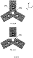
- FIG 14A and FIG 14B show a schematic side view of a majority gate device according to embodiments of the present disclosure. Due to the 3N-rotational symmetry, only two of the three input controls are visible from the side view.
- a tunnel barrier layer or non-magnetic layer 104 may be formed on and over the whole surface of the free ferromagnetic layer ( FIG 14A ) or may be formed as bottom layer of the input and/or output sensor/pillars ( FIG 14B ).
- the input controls may further comprise a fixed ferromagnetic layer atop the non-magnetic layer having a magnetization state 1181, 1182 (in the example shown being 'UP'). The majority magnetization 1021 of the free ferromagnetic layer 102 is thus 'UP' and thus the output sensor will read out a magnetization state 1191 being 'UP'.
- Control of the magnetization in the input zones of the free ferromagnetic layer could also be done or assisted by other means, such as in-plane current, spin Hall effect, Giant spin Hall effect, Rashba torque, Spin-Orbit torque, magnetic field generated by a current, magnetic field generated by additional ferromagnetic layers (stray field), Voltage Controlled Anisotropy (electric field), etc.
- Sensing of the magnetization at the output sensor could also be done by other means such as a magnetic read head, etc.
- the device could also be working when it is so small that it behaves as a macro-spin, i.e. when the ratio of the device size over the domain wall width is smaller than a certain value. In that case, the output magnetization is quickly going into the expected state thanks to the exchange interaction.
- a three dimensional stack could also be manufactured which cascades several level of majority gates according to the present disclosure on top of each other. This kind of stacking is possible due to the large range of working sizes.
- the magnetization state of the output zone 1124, 2124, 3124 could be directly transmitted to the next input zone 2121, 2122, 2123, 3121, 3122, 3123 in a higher level (above it) as shown in FIG 12A (1 st level), FIG 12B (2 nd level) and FIG 12C (3 rd level).
- the majority gate device comprises a free ferromagnetic layer which comprises a ferromagnetic material such as for example CoFe alloy, NiFe alloy, PtFe alloy, CoFeB alloy.
- a ferromagnetic material such as for example CoFe alloy, NiFe alloy, PtFe alloy, CoFeB alloy.
- the majority gate device may comprise a non-magnetic tunnel barrier layer.
- the tunnelling barrier layer may comprise an oxide selected from the group consisting of magnesium oxide, magnesium-titanium oxide, magnesium-aluminium oxide or aluminium oxide.
- the tunnelling barrier layer comprises a non-magnetic metallic material chosen from Cu, Cr or Ru.
- the output state (e.g. via an MTJ) can be detected and the corresponding signal can then be injected into a new input (e.g. via MTJ).
- This is thus a conversion of magnetic to electrical signal and vice versa. This may be done with or without amplification of the spin-polarized current.
- Another possibility is use of a magnetic strip that would serve as a bridge between the output zone and the new input zone.
Landscapes
- Physics & Mathematics (AREA)
- Engineering & Computer Science (AREA)
- Computer Hardware Design (AREA)
- Computing Systems (AREA)
- General Engineering & Computer Science (AREA)
- Mathematical Physics (AREA)
- Hall/Mr Elements (AREA)
Claims (14)
- Dispositif à porte majoritaire (2) comprenant :une couche ferromagnétique libre comprenant 3N zones d'entrée (121, 122, 123) et une seule zone de sortie en polygone (124) ayant 3N côtés, chaque zone d'entrée étant contiguë à la zone de sortie au niveau d'un côté et étant positionnée autour de la zone de sortie selon une symétrie de rotation à 3N-plis, N étant un entier supérieur à 0, de sorte que les zones d'entrée sont espacées les unes des autres par la zone de sortie ;- chaque zone d'entrée étant couplée de façon magnétique à une commande d'entrée correspondante (1181, 1182, 1183), la commande d'entrée servant à commander l'état de magnétisation de la zone d'entrée correspondante ; et- un capteur de sortie (119) couplé de façon magnétique à la zone de sortie, le capteur de sortie servant à détecter l'état de magnétisation de la zone de sortie.
- Dispositif à porte majoritaire selon la revendication 1, dans lequel la zone de sortie et chaque zone d'entrée de la matière ferromagnétique libre correspondent à un domaine magnétique, chaque domaine magnétique ayant un état de magnétisation uniforme.
- Dispositif à porte majoritaire selon la revendication 1 ou 2, dans lequel chaque commande d'entrée est couplée de façon magnétique à la zone d'entrée correspondante par une jonction à effet tunnel magnétique.
- Dispositif à porte majoritaire selon l'une quelconque des revendications précédentes, dans lequel le capteur de sortie est couplé de façon magnétique à la zone de sortie correspondante par une jonction à effet tunnel magnétique.
- Dispositif à porte majoritaire selon l'une quelconque des revendications précédentes, dans lequel chaque commande d'entrée et le capteur de sortie sont des piliers circulaires.
- Dispositif à porte majoritaire selon l'une quelconque des revendications précédentes, dans lequel la distance entre chaque commande d'entrée et le capteur de sortie est plus petite que 400 nm.
- Dispositif à porte majoritaire selon l'une quelconque des revendications précédentes, dans lequel chaque zone d'entrée est subdivisée en sous-zones d'entrée voisines, la commande d'entrée correspondante de la zone d'entrée étant couplée de façon magnétique à une des sous-zones d'entrée, et le dispositif à porte majoritaire comprend en outre pour chaque sous-zone d'entrée restante une autre commande d'entrée correspondante, l'autre commande d'entrée étant couplée de façon magnétique à sa sous-zone d'entrée correspondante et les commandes d'entrée de chaque sous-zone d'entrée étant électriquement reliée.
- Dispositif à porte majoritaire selon l'une quelconque des revendications précédentes, dans lequel la zone d'entrée a une forme choisie parmi un trapézoïde isocèle, un rectangle, un carré, un triangle, un segment ou un demi-cercle.
- Dispositif à porte majoritaire selon l'une quelconque des revendications précédentes, dans lequel la largeur de la zone d'entrée diminue vers la zone de sortie.
- Dispositif tridimensionnel à porte majoritaire comprenant une seconde couche de dispositifs à porte majoritaire selon l'une quelconque des revendications précédentes empilée sur une première couche de dispositifs à porte majoritaire selon l'une quelconque des revendications précédentes dans lequel la zone de sortie de chaque dispositif à porte majoritaire de la première couche est reliée à une zone d'entrée d'un dispositif à porte majoritaire de la seconde couche.
- Procédé pour mettre en oeuvre le dispositif à porte majoritaire selon l'une quelconque des revendications précédentes, comprenant :- l'application d'une tension prédéterminée à chaque commande d'entrée ; et- après cela, la détermination de l'effet combiné des tensions prédéterminées sur l'état de magnétisation de la zone de sortie.
- Procédé pour mettre en oeuvre un dispositif à porte majoritaire selon la revendication 11, dans lequel l'état de magnétisation de la zone de sortie est égal à l'état de magnétisation majoritaire des zones d'entrée.
- Procédé pour mettre en oeuvre un dispositif à porte majoritaire selon la revendication 11 ou 12, dans lequel l'effet combiné des tensions prédéterminées induit la mise en contiguïté d'au moins deux parois de domaine et la propagation des parois de domaine rendues contiguës entièrement par la zone de sortie.
- Procédé pour mettre en oeuvre un dispositif à porte majoritaire selon les revendications 11 à 13, dans lequel l'état de magnétisation des zones d'entrée est commandé par un courant dans le plan, un effet Hall de spin, un effet Hall de spin Giant, un couple Rashba, un couple spin-orbite, un champ magnétique produit par un courant, un champ magnétique produit par des couches ferromagnétiques supplémentaires (champ parasite) ou une Anisotropie Commandée en Tension (champ électrique).
Priority Applications (3)
| Application Number | Priority Date | Filing Date | Title |
|---|---|---|---|
| EP14192272.4A EP3016287B1 (fr) | 2014-11-03 | 2014-11-07 | Dispositif de porte majoritaire à couple de spin |
| PCT/EP2015/075552 WO2016071319A1 (fr) | 2014-11-03 | 2015-11-03 | Dispositif de porte majoritaire à couple de rotation |
| US15/586,165 US9979402B2 (en) | 2014-11-03 | 2017-05-03 | Spin torque majority gate device |
Applications Claiming Priority (2)
| Application Number | Priority Date | Filing Date | Title |
|---|---|---|---|
| EP14191541 | 2014-11-03 | ||
| EP14192272.4A EP3016287B1 (fr) | 2014-11-03 | 2014-11-07 | Dispositif de porte majoritaire à couple de spin |
Publications (2)
| Publication Number | Publication Date |
|---|---|
| EP3016287A1 EP3016287A1 (fr) | 2016-05-04 |
| EP3016287B1 true EP3016287B1 (fr) | 2017-04-26 |
Family
ID=51868046
Family Applications (1)
| Application Number | Title | Priority Date | Filing Date |
|---|---|---|---|
| EP14192272.4A Active EP3016287B1 (fr) | 2014-11-03 | 2014-11-07 | Dispositif de porte majoritaire à couple de spin |
Country Status (3)
| Country | Link |
|---|---|
| US (1) | US9979402B2 (fr) |
| EP (1) | EP3016287B1 (fr) |
| WO (1) | WO2016071319A1 (fr) |
Families Citing this family (12)
| Publication number | Priority date | Publication date | Assignee | Title |
|---|---|---|---|---|
| FR3031622B1 (fr) * | 2015-01-14 | 2018-02-16 | Centre National De La Recherche Scientifique | Point memoire magnetique |
| US10269402B2 (en) * | 2015-09-15 | 2019-04-23 | Imec Vzw | Magnetic topological soliton detection |
| CN107800426B (zh) * | 2016-08-31 | 2023-07-25 | Imec 非营利协会 | 磁性多数决定门 |
| US10236046B2 (en) * | 2016-11-09 | 2019-03-19 | Imec Vzw | Method of propagating magnetic domain wall in magnetic devices |
| US10593414B2 (en) * | 2016-11-09 | 2020-03-17 | Imec Vzw | Method of propagating magnetic domain wall in magnetic devices |
| EP3503231B1 (fr) * | 2017-12-19 | 2021-11-24 | IMEC vzw | Dispositif à couple de transfert de spin |
| US11187764B2 (en) * | 2020-03-20 | 2021-11-30 | Allegro Microsystems, Llc | Layout of magnetoresistance element |
| KR102284925B1 (ko) | 2020-05-07 | 2021-08-03 | 한국과학기술원 | 자기 로직 소자 |
| KR102376380B1 (ko) * | 2020-09-10 | 2022-03-18 | 재단법인대구경북과학기술원 | 자구벽 이동에 기반한 스핀 토크 다수결 게이트 |
| US12302586B2 (en) * | 2023-03-28 | 2025-05-13 | Hanberry LLC | Nanomagnetic data storage and processing devices |
| US12248039B2 (en) | 2023-08-08 | 2025-03-11 | Allegro Microsystems, Llc | Interleaving sub-arrays of magnetoresistance elements based on reference directions to compensate for bridge offset |
| KR102755195B1 (ko) * | 2023-10-05 | 2025-01-21 | 인하대학교 산학협력단 | 스핀 토크 다수 게이트의 동적 로직 스타일 기반 에너지 효율적 로직 |
Family Cites Families (4)
| Publication number | Priority date | Publication date | Assignee | Title |
|---|---|---|---|---|
| JP5288293B2 (ja) * | 2008-08-25 | 2013-09-11 | 日本電気株式会社 | 磁気抵抗素子、論理ゲート、及び論理ゲートの動作方法 |
| US8450818B2 (en) | 2009-06-18 | 2013-05-28 | Dmitri E. Nikonov | Methods of forming spin torque devices and structures formed thereby |
| US8063460B2 (en) * | 2009-12-18 | 2011-11-22 | Intel Corporation | Spin torque magnetic integrated circuits and devices therefor |
| US8198919B1 (en) * | 2011-02-23 | 2012-06-12 | The Regengs of the University of California | Spin transfer torque triad for non-volatile logic gates |
-
2014
- 2014-11-07 EP EP14192272.4A patent/EP3016287B1/fr active Active
-
2015
- 2015-11-03 WO PCT/EP2015/075552 patent/WO2016071319A1/fr not_active Ceased
-
2017
- 2017-05-03 US US15/586,165 patent/US9979402B2/en active Active
Non-Patent Citations (1)
| Title |
|---|
| None * |
Also Published As
| Publication number | Publication date |
|---|---|
| US20170302280A1 (en) | 2017-10-19 |
| EP3016287A1 (fr) | 2016-05-04 |
| US9979402B2 (en) | 2018-05-22 |
| WO2016071319A1 (fr) | 2016-05-12 |
Similar Documents
| Publication | Publication Date | Title |
|---|---|---|
| EP3016287B1 (fr) | Dispositif de porte majoritaire à couple de spin | |
| KR102611084B1 (ko) | 전압 제어 층간 교환 결합 자기저항 메모리 디바이스 및 그의 동작 방법 | |
| JP6168578B2 (ja) | 磁気抵抗効果素子、及び磁気メモリ装置 | |
| CN100565701C (zh) | 磁电阻随机存取存储器 | |
| US10230046B2 (en) | Magnetoresistive structure having two dielectric layers, and method of manufacturing same | |
| TWI592930B (zh) | 自旋力矩磁性積體電路及其製造方法 | |
| KR100875383B1 (ko) | 보텍스 자기 랜덤 액세스 메모리 | |
| US9300301B2 (en) | Nonvolatile magnetic logic device | |
| EP1490877B1 (fr) | Couche de detection ferrimagnetique synthetique pour applications magnetiques a acces aleatoire (mram) | |
| CN102916123A (zh) | 具有多电平的磁阻存储装置及其驱动方法 | |
| Liu et al. | Magnetic–electrical interface for nanomagnet logic | |
| JP2008243933A (ja) | 磁気ランダムアクセスメモリおよびこれを備えた記録装置 | |
| EP3035347B1 (fr) | Dispositif de porte majoritaire à couple de spin | |
| CN105679358A (zh) | 垂直型自旋转移矩磁性随机存储器记忆单元 | |
| JP2024092593A (ja) | 多値磁気メモリ素子、磁気メモリ装置、多値磁気メモリ素子の制御方法、および制御プログラム | |
| WO2016079085A1 (fr) | Élément de mémoire magnétique à multiples grilles à anisotropie magnétique en commande de tension (vcma) et procédé de fonctionnement d'un tel élément de mémoire | |
| CN105633109A (zh) | 磁性随机存储器记忆单元及其读写和抗干扰方法 | |
| CN117412663A (zh) | 手性切换驱动的自旋力矩逻辑门 | |
| US9257970B1 (en) | Magnetic latch | |
| DeAngelis | Spin-Valve Interface for Magnetic Quantum Dot Cellular Automata |
Legal Events
| Date | Code | Title | Description |
|---|---|---|---|
| PUAI | Public reference made under article 153(3) epc to a published international application that has entered the european phase |
Free format text: ORIGINAL CODE: 0009012 |
|
| AK | Designated contracting states |
Kind code of ref document: A1 Designated state(s): AL AT BE BG CH CY CZ DE DK EE ES FI FR GB GR HR HU IE IS IT LI LT LU LV MC MK MT NL NO PL PT RO RS SE SI SK SM TR |
|
| AX | Request for extension of the european patent |
Extension state: BA ME |
|
| 17P | Request for examination filed |
Effective date: 20161014 |
|
| RBV | Designated contracting states (corrected) |
Designated state(s): AL AT BE BG CH CY CZ DE DK EE ES FI FR GB GR HR HU IE IS IT LI LT LU LV MC MK MT NL NO PL PT RO RS SE SI SK SM TR |
|
| GRAP | Despatch of communication of intention to grant a patent |
Free format text: ORIGINAL CODE: EPIDOSNIGR1 |
|
| GRAS | Grant fee paid |
Free format text: ORIGINAL CODE: EPIDOSNIGR3 |
|
| GRAA | (expected) grant |
Free format text: ORIGINAL CODE: 0009210 |
|
| INTG | Intention to grant announced |
Effective date: 20170301 |
|
| RIN1 | Information on inventor provided before grant (corrected) |
Inventor name: POURTOIS, GEOFFREY Inventor name: RADU, IULIANA Inventor name: VAYSSET, ADRIEN |
|
| AK | Designated contracting states |
Kind code of ref document: B1 Designated state(s): AL AT BE BG CH CY CZ DE DK EE ES FI FR GB GR HR HU IE IS IT LI LT LU LV MC MK MT NL NO PL PT RO RS SE SI SK SM TR |
|
| REG | Reference to a national code |
Ref country code: GB Ref legal event code: FG4D |
|
| REG | Reference to a national code |
Ref country code: CH Ref legal event code: EP |
|
| REG | Reference to a national code |
Ref country code: AT Ref legal event code: REF Ref document number: 888675 Country of ref document: AT Kind code of ref document: T Effective date: 20170515 |
|
| REG | Reference to a national code |
Ref country code: IE Ref legal event code: FG4D |
|
| REG | Reference to a national code |
Ref country code: DE Ref legal event code: R096 Ref document number: 602014008994 Country of ref document: DE |
|
| REG | Reference to a national code |
Ref country code: NL Ref legal event code: MP Effective date: 20170426 |
|
| REG | Reference to a national code |
Ref country code: LT Ref legal event code: MG4D |
|
| REG | Reference to a national code |
Ref country code: AT Ref legal event code: MK05 Ref document number: 888675 Country of ref document: AT Kind code of ref document: T Effective date: 20170426 |
|
| PG25 | Lapsed in a contracting state [announced via postgrant information from national office to epo] |
Ref country code: NL Free format text: LAPSE BECAUSE OF FAILURE TO SUBMIT A TRANSLATION OF THE DESCRIPTION OR TO PAY THE FEE WITHIN THE PRESCRIBED TIME-LIMIT Effective date: 20170426 |
|
| REG | Reference to a national code |
Ref country code: FR Ref legal event code: PLFP Year of fee payment: 4 |
|
| PG25 | Lapsed in a contracting state [announced via postgrant information from national office to epo] |
Ref country code: AT Free format text: LAPSE BECAUSE OF FAILURE TO SUBMIT A TRANSLATION OF THE DESCRIPTION OR TO PAY THE FEE WITHIN THE PRESCRIBED TIME-LIMIT Effective date: 20170426 Ref country code: ES Free format text: LAPSE BECAUSE OF FAILURE TO SUBMIT A TRANSLATION OF THE DESCRIPTION OR TO PAY THE FEE WITHIN THE PRESCRIBED TIME-LIMIT Effective date: 20170426 Ref country code: NO Free format text: LAPSE BECAUSE OF FAILURE TO SUBMIT A TRANSLATION OF THE DESCRIPTION OR TO PAY THE FEE WITHIN THE PRESCRIBED TIME-LIMIT Effective date: 20170726 Ref country code: FI Free format text: LAPSE BECAUSE OF FAILURE TO SUBMIT A TRANSLATION OF THE DESCRIPTION OR TO PAY THE FEE WITHIN THE PRESCRIBED TIME-LIMIT Effective date: 20170426 Ref country code: LT Free format text: LAPSE BECAUSE OF FAILURE TO SUBMIT A TRANSLATION OF THE DESCRIPTION OR TO PAY THE FEE WITHIN THE PRESCRIBED TIME-LIMIT Effective date: 20170426 Ref country code: GR Free format text: LAPSE BECAUSE OF FAILURE TO SUBMIT A TRANSLATION OF THE DESCRIPTION OR TO PAY THE FEE WITHIN THE PRESCRIBED TIME-LIMIT Effective date: 20170727 Ref country code: HR Free format text: LAPSE BECAUSE OF FAILURE TO SUBMIT A TRANSLATION OF THE DESCRIPTION OR TO PAY THE FEE WITHIN THE PRESCRIBED TIME-LIMIT Effective date: 20170426 |
|
| PG25 | Lapsed in a contracting state [announced via postgrant information from national office to epo] |
Ref country code: BG Free format text: LAPSE BECAUSE OF FAILURE TO SUBMIT A TRANSLATION OF THE DESCRIPTION OR TO PAY THE FEE WITHIN THE PRESCRIBED TIME-LIMIT Effective date: 20170726 Ref country code: LV Free format text: LAPSE BECAUSE OF FAILURE TO SUBMIT A TRANSLATION OF THE DESCRIPTION OR TO PAY THE FEE WITHIN THE PRESCRIBED TIME-LIMIT Effective date: 20170426 Ref country code: IS Free format text: LAPSE BECAUSE OF FAILURE TO SUBMIT A TRANSLATION OF THE DESCRIPTION OR TO PAY THE FEE WITHIN THE PRESCRIBED TIME-LIMIT Effective date: 20170826 Ref country code: PL Free format text: LAPSE BECAUSE OF FAILURE TO SUBMIT A TRANSLATION OF THE DESCRIPTION OR TO PAY THE FEE WITHIN THE PRESCRIBED TIME-LIMIT Effective date: 20170426 Ref country code: RS Free format text: LAPSE BECAUSE OF FAILURE TO SUBMIT A TRANSLATION OF THE DESCRIPTION OR TO PAY THE FEE WITHIN THE PRESCRIBED TIME-LIMIT Effective date: 20170426 Ref country code: SE Free format text: LAPSE BECAUSE OF FAILURE TO SUBMIT A TRANSLATION OF THE DESCRIPTION OR TO PAY THE FEE WITHIN THE PRESCRIBED TIME-LIMIT Effective date: 20170426 |
|
| REG | Reference to a national code |
Ref country code: DE Ref legal event code: R097 Ref document number: 602014008994 Country of ref document: DE |
|
| PG25 | Lapsed in a contracting state [announced via postgrant information from national office to epo] |
Ref country code: EE Free format text: LAPSE BECAUSE OF FAILURE TO SUBMIT A TRANSLATION OF THE DESCRIPTION OR TO PAY THE FEE WITHIN THE PRESCRIBED TIME-LIMIT Effective date: 20170426 Ref country code: RO Free format text: LAPSE BECAUSE OF FAILURE TO SUBMIT A TRANSLATION OF THE DESCRIPTION OR TO PAY THE FEE WITHIN THE PRESCRIBED TIME-LIMIT Effective date: 20170426 Ref country code: SK Free format text: LAPSE BECAUSE OF FAILURE TO SUBMIT A TRANSLATION OF THE DESCRIPTION OR TO PAY THE FEE WITHIN THE PRESCRIBED TIME-LIMIT Effective date: 20170426 Ref country code: CZ Free format text: LAPSE BECAUSE OF FAILURE TO SUBMIT A TRANSLATION OF THE DESCRIPTION OR TO PAY THE FEE WITHIN THE PRESCRIBED TIME-LIMIT Effective date: 20170426 Ref country code: DK Free format text: LAPSE BECAUSE OF FAILURE TO SUBMIT A TRANSLATION OF THE DESCRIPTION OR TO PAY THE FEE WITHIN THE PRESCRIBED TIME-LIMIT Effective date: 20170426 |
|
| PG25 | Lapsed in a contracting state [announced via postgrant information from national office to epo] |
Ref country code: SM Free format text: LAPSE BECAUSE OF FAILURE TO SUBMIT A TRANSLATION OF THE DESCRIPTION OR TO PAY THE FEE WITHIN THE PRESCRIBED TIME-LIMIT Effective date: 20170426 Ref country code: IT Free format text: LAPSE BECAUSE OF FAILURE TO SUBMIT A TRANSLATION OF THE DESCRIPTION OR TO PAY THE FEE WITHIN THE PRESCRIBED TIME-LIMIT Effective date: 20170426 |
|
| PLBE | No opposition filed within time limit |
Free format text: ORIGINAL CODE: 0009261 |
|
| STAA | Information on the status of an ep patent application or granted ep patent |
Free format text: STATUS: NO OPPOSITION FILED WITHIN TIME LIMIT |
|
| 26N | No opposition filed |
Effective date: 20180129 |
|
| PG25 | Lapsed in a contracting state [announced via postgrant information from national office to epo] |
Ref country code: SI Free format text: LAPSE BECAUSE OF FAILURE TO SUBMIT A TRANSLATION OF THE DESCRIPTION OR TO PAY THE FEE WITHIN THE PRESCRIBED TIME-LIMIT Effective date: 20170426 |
|
| PG25 | Lapsed in a contracting state [announced via postgrant information from national office to epo] |
Ref country code: MC Free format text: LAPSE BECAUSE OF FAILURE TO SUBMIT A TRANSLATION OF THE DESCRIPTION OR TO PAY THE FEE WITHIN THE PRESCRIBED TIME-LIMIT Effective date: 20170426 |
|
| PG25 | Lapsed in a contracting state [announced via postgrant information from national office to epo] |
Ref country code: LI Free format text: LAPSE BECAUSE OF NON-PAYMENT OF DUE FEES Effective date: 20171130 Ref country code: CH Free format text: LAPSE BECAUSE OF NON-PAYMENT OF DUE FEES Effective date: 20171130 |
|
| PG25 | Lapsed in a contracting state [announced via postgrant information from national office to epo] |
Ref country code: LU Free format text: LAPSE BECAUSE OF NON-PAYMENT OF DUE FEES Effective date: 20171107 |
|
| REG | Reference to a national code |
Ref country code: BE Ref legal event code: MM Effective date: 20171130 |
|
| REG | Reference to a national code |
Ref country code: IE Ref legal event code: MM4A |
|
| PG25 | Lapsed in a contracting state [announced via postgrant information from national office to epo] |
Ref country code: MT Free format text: LAPSE BECAUSE OF NON-PAYMENT OF DUE FEES Effective date: 20171107 |
|
| REG | Reference to a national code |
Ref country code: FR Ref legal event code: PLFP Year of fee payment: 5 |
|
| PG25 | Lapsed in a contracting state [announced via postgrant information from national office to epo] |
Ref country code: IE Free format text: LAPSE BECAUSE OF NON-PAYMENT OF DUE FEES Effective date: 20171107 |
|
| PG25 | Lapsed in a contracting state [announced via postgrant information from national office to epo] |
Ref country code: BE Free format text: LAPSE BECAUSE OF NON-PAYMENT OF DUE FEES Effective date: 20171130 |
|
| PG25 | Lapsed in a contracting state [announced via postgrant information from national office to epo] |
Ref country code: HU Free format text: LAPSE BECAUSE OF FAILURE TO SUBMIT A TRANSLATION OF THE DESCRIPTION OR TO PAY THE FEE WITHIN THE PRESCRIBED TIME-LIMIT; INVALID AB INITIO Effective date: 20141107 |
|
| GBPC | Gb: european patent ceased through non-payment of renewal fee |
Effective date: 20181107 |
|
| PG25 | Lapsed in a contracting state [announced via postgrant information from national office to epo] |
Ref country code: CY Free format text: LAPSE BECAUSE OF FAILURE TO SUBMIT A TRANSLATION OF THE DESCRIPTION OR TO PAY THE FEE WITHIN THE PRESCRIBED TIME-LIMIT Effective date: 20170426 |
|
| PG25 | Lapsed in a contracting state [announced via postgrant information from national office to epo] |
Ref country code: MK Free format text: LAPSE BECAUSE OF FAILURE TO SUBMIT A TRANSLATION OF THE DESCRIPTION OR TO PAY THE FEE WITHIN THE PRESCRIBED TIME-LIMIT Effective date: 20170426 |
|
| PG25 | Lapsed in a contracting state [announced via postgrant information from national office to epo] |
Ref country code: GB Free format text: LAPSE BECAUSE OF NON-PAYMENT OF DUE FEES Effective date: 20181107 |
|
| PG25 | Lapsed in a contracting state [announced via postgrant information from national office to epo] |
Ref country code: TR Free format text: LAPSE BECAUSE OF FAILURE TO SUBMIT A TRANSLATION OF THE DESCRIPTION OR TO PAY THE FEE WITHIN THE PRESCRIBED TIME-LIMIT Effective date: 20170426 |
|
| PG25 | Lapsed in a contracting state [announced via postgrant information from national office to epo] |
Ref country code: PT Free format text: LAPSE BECAUSE OF FAILURE TO SUBMIT A TRANSLATION OF THE DESCRIPTION OR TO PAY THE FEE WITHIN THE PRESCRIBED TIME-LIMIT Effective date: 20170426 |
|
| PG25 | Lapsed in a contracting state [announced via postgrant information from national office to epo] |
Ref country code: AL Free format text: LAPSE BECAUSE OF FAILURE TO SUBMIT A TRANSLATION OF THE DESCRIPTION OR TO PAY THE FEE WITHIN THE PRESCRIBED TIME-LIMIT Effective date: 20170426 |
|
| P01 | Opt-out of the competence of the unified patent court (upc) registered |
Effective date: 20230513 |
|
| PGFP | Annual fee paid to national office [announced via postgrant information from national office to epo] |
Ref country code: DE Payment date: 20251022 Year of fee payment: 12 |
|
| PGFP | Annual fee paid to national office [announced via postgrant information from national office to epo] |
Ref country code: FR Payment date: 20251022 Year of fee payment: 12 |