EP3020075B1 - Systèmes capteurs de proximité et leurs procédés de fonctionnement - Google Patents
Systèmes capteurs de proximité et leurs procédés de fonctionnement Download PDFInfo
- Publication number
- EP3020075B1 EP3020075B1 EP14898353.9A EP14898353A EP3020075B1 EP 3020075 B1 EP3020075 B1 EP 3020075B1 EP 14898353 A EP14898353 A EP 14898353A EP 3020075 B1 EP3020075 B1 EP 3020075B1
- Authority
- EP
- European Patent Office
- Prior art keywords
- photo detector
- region
- proximity sensor
- sensor system
- light
- Prior art date
- Legal status (The legal status is an assumption and is not a legal conclusion. Google has not performed a legal analysis and makes no representation as to the accuracy of the status listed.)
- Active
Links
Images

















Classifications
-
- G—PHYSICS
- G01—MEASURING; TESTING
- G01J—MEASUREMENT OF INTENSITY, VELOCITY, SPECTRAL CONTENT, POLARISATION, PHASE OR PULSE CHARACTERISTICS OF INFRARED, VISIBLE OR ULTRAVIOLET LIGHT; COLORIMETRY; RADIATION PYROMETRY
- G01J3/00—Spectrometry; Spectrophotometry; Monochromators; Measuring colours
- G01J3/02—Details
- G01J3/0256—Compact construction
- G01J3/0259—Monolithic
-
- G—PHYSICS
- G01—MEASURING; TESTING
- G01S—RADIO DIRECTION-FINDING; RADIO NAVIGATION; DETERMINING DISTANCE OR VELOCITY BY USE OF RADIO WAVES; LOCATING OR PRESENCE-DETECTING BY USE OF THE REFLECTION OR RERADIATION OF RADIO WAVES; ANALOGOUS ARRANGEMENTS USING OTHER WAVES
- G01S17/00—Systems using the reflection or reradiation of electromagnetic waves other than radio waves, e.g. lidar systems
- G01S17/02—Systems using the reflection of electromagnetic waves other than radio waves
- G01S17/04—Systems determining the presence of a target
-
- G—PHYSICS
- G01—MEASURING; TESTING
- G01S—RADIO DIRECTION-FINDING; RADIO NAVIGATION; DETERMINING DISTANCE OR VELOCITY BY USE OF RADIO WAVES; LOCATING OR PRESENCE-DETECTING BY USE OF THE REFLECTION OR RERADIATION OF RADIO WAVES; ANALOGOUS ARRANGEMENTS USING OTHER WAVES
- G01S17/00—Systems using the reflection or reradiation of electromagnetic waves other than radio waves, e.g. lidar systems
- G01S17/02—Systems using the reflection of electromagnetic waves other than radio waves
- G01S17/06—Systems determining position data of a target
- G01S17/08—Systems determining position data of a target for measuring distance only
- G01S17/10—Systems determining position data of a target for measuring distance only using transmission of interrupted, pulse-modulated waves
- G01S17/18—Systems determining position data of a target for measuring distance only using transmission of interrupted, pulse-modulated waves wherein range gates are used
-
- G—PHYSICS
- G01—MEASURING; TESTING
- G01S—RADIO DIRECTION-FINDING; RADIO NAVIGATION; DETERMINING DISTANCE OR VELOCITY BY USE OF RADIO WAVES; LOCATING OR PRESENCE-DETECTING BY USE OF THE REFLECTION OR RERADIATION OF RADIO WAVES; ANALOGOUS ARRANGEMENTS USING OTHER WAVES
- G01S7/00—Details of systems according to groups G01S13/00, G01S15/00, G01S17/00
- G01S7/48—Details of systems according to groups G01S13/00, G01S15/00, G01S17/00 of systems according to group G01S17/00
- G01S7/481—Constructional features, e.g. arrangements of optical elements
- G01S7/4818—Constructional features, e.g. arrangements of optical elements using optical fibres
-
- G—PHYSICS
- G01—MEASURING; TESTING
- G01S—RADIO DIRECTION-FINDING; RADIO NAVIGATION; DETERMINING DISTANCE OR VELOCITY BY USE OF RADIO WAVES; LOCATING OR PRESENCE-DETECTING BY USE OF THE REFLECTION OR RERADIATION OF RADIO WAVES; ANALOGOUS ARRANGEMENTS USING OTHER WAVES
- G01S7/00—Details of systems according to groups G01S13/00, G01S15/00, G01S17/00
- G01S7/48—Details of systems according to groups G01S13/00, G01S15/00, G01S17/00 of systems according to group G01S17/00
- G01S7/483—Details of pulse systems
- G01S7/486—Receivers
- G01S7/4861—Circuits for detection, sampling, integration or read-out
- G01S7/4863—Detector arrays, e.g. charge-transfer gates
-
- G—PHYSICS
- G01—MEASURING; TESTING
- G01S—RADIO DIRECTION-FINDING; RADIO NAVIGATION; DETERMINING DISTANCE OR VELOCITY BY USE OF RADIO WAVES; LOCATING OR PRESENCE-DETECTING BY USE OF THE REFLECTION OR RERADIATION OF RADIO WAVES; ANALOGOUS ARRANGEMENTS USING OTHER WAVES
- G01S7/00—Details of systems according to groups G01S13/00, G01S15/00, G01S17/00
- G01S7/48—Details of systems according to groups G01S13/00, G01S15/00, G01S17/00 of systems according to group G01S17/00
- G01S7/483—Details of pulse systems
- G01S7/486—Receivers
- G01S7/4865—Time delay measurement, e.g. time-of-flight measurement, time of arrival measurement or determining the exact position of a peak
-
- H—ELECTRICITY
- H10—SEMICONDUCTOR DEVICES; ELECTRIC SOLID-STATE DEVICES NOT OTHERWISE PROVIDED FOR
- H10F—INORGANIC SEMICONDUCTOR DEVICES SENSITIVE TO INFRARED RADIATION, LIGHT, ELECTROMAGNETIC RADIATION OF SHORTER WAVELENGTH OR CORPUSCULAR RADIATION
- H10F30/00—Individual radiation-sensitive semiconductor devices in which radiation controls the flow of current through the devices, e.g. photodetectors
- H10F30/20—Individual radiation-sensitive semiconductor devices in which radiation controls the flow of current through the devices, e.g. photodetectors the devices having potential barriers, e.g. phototransistors
- H10F30/21—Individual radiation-sensitive semiconductor devices in which radiation controls the flow of current through the devices, e.g. photodetectors the devices having potential barriers, e.g. phototransistors the devices being sensitive to infrared, visible or ultraviolet radiation
- H10F30/22—Individual radiation-sensitive semiconductor devices in which radiation controls the flow of current through the devices, e.g. photodetectors the devices having potential barriers, e.g. phototransistors the devices being sensitive to infrared, visible or ultraviolet radiation the devices having only one potential barrier, e.g. photodiodes
- H10F30/223—Individual radiation-sensitive semiconductor devices in which radiation controls the flow of current through the devices, e.g. photodetectors the devices having potential barriers, e.g. phototransistors the devices being sensitive to infrared, visible or ultraviolet radiation the devices having only one potential barrier, e.g. photodiodes the potential barrier being a PIN barrier
-
- H—ELECTRICITY
- H10—SEMICONDUCTOR DEVICES; ELECTRIC SOLID-STATE DEVICES NOT OTHERWISE PROVIDED FOR
- H10F—INORGANIC SEMICONDUCTOR DEVICES SENSITIVE TO INFRARED RADIATION, LIGHT, ELECTROMAGNETIC RADIATION OF SHORTER WAVELENGTH OR CORPUSCULAR RADIATION
- H10F30/00—Individual radiation-sensitive semiconductor devices in which radiation controls the flow of current through the devices, e.g. photodetectors
- H10F30/20—Individual radiation-sensitive semiconductor devices in which radiation controls the flow of current through the devices, e.g. photodetectors the devices having potential barriers, e.g. phototransistors
- H10F30/21—Individual radiation-sensitive semiconductor devices in which radiation controls the flow of current through the devices, e.g. photodetectors the devices having potential barriers, e.g. phototransistors the devices being sensitive to infrared, visible or ultraviolet radiation
- H10F30/28—Individual radiation-sensitive semiconductor devices in which radiation controls the flow of current through the devices, e.g. photodetectors the devices having potential barriers, e.g. phototransistors the devices being sensitive to infrared, visible or ultraviolet radiation the devices being characterised by field-effect operation, e.g. junction field-effect phototransistors
-
- H—ELECTRICITY
- H10—SEMICONDUCTOR DEVICES; ELECTRIC SOLID-STATE DEVICES NOT OTHERWISE PROVIDED FOR
- H10F—INORGANIC SEMICONDUCTOR DEVICES SENSITIVE TO INFRARED RADIATION, LIGHT, ELECTROMAGNETIC RADIATION OF SHORTER WAVELENGTH OR CORPUSCULAR RADIATION
- H10F55/00—Radiation-sensitive semiconductor devices covered by groups H10F10/00, H10F19/00 or H10F30/00 being structurally associated with electric light sources and electrically or optically coupled thereto
- H10F55/20—Radiation-sensitive semiconductor devices covered by groups H10F10/00, H10F19/00 or H10F30/00 being structurally associated with electric light sources and electrically or optically coupled thereto wherein the electric light source controls the radiation-sensitive semiconductor devices, e.g. optocouplers
- H10F55/25—Radiation-sensitive semiconductor devices covered by groups H10F10/00, H10F19/00 or H10F30/00 being structurally associated with electric light sources and electrically or optically coupled thereto wherein the electric light source controls the radiation-sensitive semiconductor devices, e.g. optocouplers wherein the radiation-sensitive devices and the electric light source are all semiconductor devices
-
- H—ELECTRICITY
- H10—SEMICONDUCTOR DEVICES; ELECTRIC SOLID-STATE DEVICES NOT OTHERWISE PROVIDED FOR
- H10F—INORGANIC SEMICONDUCTOR DEVICES SENSITIVE TO INFRARED RADIATION, LIGHT, ELECTROMAGNETIC RADIATION OF SHORTER WAVELENGTH OR CORPUSCULAR RADIATION
- H10F77/00—Constructional details of devices covered by this subclass
- H10F77/95—Circuit arrangements
- H10F77/953—Circuit arrangements for devices having potential barriers
Definitions
- the present invention relates generally to proximity sensors and, more particularly, to techniques for using photo detectors as tunable proximity sensors for detection of target objects and ascertaining their distance from the proximity sensors.
- the present embodiments relate to, among other things, a tunable proximity sensor system comprising monolithic detectors or sensors to detect target objects by detecting reflected light incident on the sensors and, in response thereto, to generate an electrical signal.
- the present embodiments relate to methods of controlling such proximity sensors to meet or accommodate response time specifications as well as power consumption specifications.
- JP 2011 007622 discloses a sensor apparatus for detecting an illuminance of an ambient light at a wide dynamic range and a high resolution; and also detecting the existence of an adjacent object.
- US 2007/103748 disclose a light detecting element and control method of a light detecting element.
- US 2006/192938 discloses a distance image sensor.
- the techniques are realized as a proximity sensor system including a photo detector having a first doped region, a gate, a second doped region and a light absorbing region, wherein the light absorbing region includes at least one material in which, in response to light incident thereon, carrier pairs of opposite charge are generated, wherein the first doped region attracts a first carrier of the carrier pairs having a first charge, wherein the second doped region attracts a second carrier of the carrier pairs having a second opposite charge, and wherein the photo detector generates an output signal indicative of the presence of an object in a vicinity of the proximity sensor system.
- This embodiment also includes a control circuitry for generating a plurality of control signals to be applied to the photo detector, wherein the plurality of control signals comprises a first control signal applied to the first doped region of the photo detector, a second control signal applied to the gate of the photo detector, and a third control signal applied to the second doped region of the photo detector; wherein the applied control signals control an operating state of the photo detector.
- This embodiment further includes a signal detector to detect the output signal from the photo detector.
- the first doped region of the photo detector is formed of a p-type semiconductor and the second doped region is formed of an n-type semiconductor.
- control circuitry places the photo detector in a non-detecting state by generating a first set of relative voltage amplitudes for the first, second, and third control signals so that the photo detector is in a reverse bias mode with substantially no current flow in the photo detector.
- first voltage amplitude applied to the first doped region is less than the third voltage amplitude applied to the second doped region.
- the control circuitry places the photo detector in a detecting state by generating a second set of relative voltage amplitudes for the first, second, and third control signals so that the photo detector is in a forward bias mode with substantially no current flow in the photo detector in the absence of incident light on the photo detector.
- the first voltage amplitude applied to the first doped region differs from the third voltage amplitude applied to the second doped region by approximately 1 volt..
- the control circuitry places the photo detector in a detecting state by generating a second set of relative voltage amplitudes of the first, second, and third control signals so that the photo detector is in a forward bias mode with current flow in the photo detector in the presence of incident light on the photo detector.
- increasing an electric field between the first and second doped regions reduces a time for the current flow in the photo detector in response to the incident light.
- decreasing an electric field between the first and second doped regions increases a time for the current flow in the photo detector in response to the incident light.
- the control circuitry applies the control signals to alternate the photo detector between a non-detecting state and a detecting state.
- the control circuitry places the photo detector in the non-detecting state by generating a first set of relative voltage amplitudes of the first, second, and third control signals so that the photo detector is in a reverse bias mode with substantially no current flow.
- the control circuitry places the photo detector in the detecting state by generating a second set of relative voltage amplitudes of the first, second, and third control signals so that the photo detector is in a forward biased mode with substantially no current flow in absence of incident light and with current flow in presence of incident light.
- a proximity sensor system further including a pulsing light source.
- the pulsing of the light source of the proximity sensor system is synchronized with the photo detector and emits light when the photo detector is in a detecting state.
- the techniques may be realized as a method for detecting a presence of a target using the proximity sensor system according to any of the preceding embodiments, wherein a time between the emission from the light source and the detection of current flow in the photo detector, due to incident reflected light from the target, is used to detect the presence of the target.
- the techniques may be realized as a method of detecting a distance of a target using the proximity sensor system according to any of the preceding embodiments, wherein a time between the emission from the light source and the detection of current flow in the photo detector, due to incident reflected light from the target, is used to ascertain the distance of the target.
- the present invention is directed to a proximity sensor system and methods of operations thereof.
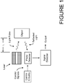
- the proximity sensor system includes one or more lasers to generate light (for example, a plurality of light pulses) that are directed to an object.
- the system further includes one or more photo detectors to detect light (for example, one or more the laser light pulses) reflected from the object.
- the control circuitry generates control signals and applies such control signals to the photo detector, which, in response, places the photo detector in a sensing mode. While in the sensing mode, the photo detector is capable of detecting light incident thereon.
- a signal detector receives the output of the photo detector and, in one embodiment, determines when reflected light has detected.
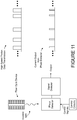
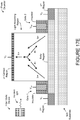
- FIGURE 2 illustrates a timing relationship between the laser output (here depicted as a pulse) and photo detector (enabling and detection) of the proximity sensor system according to certain aspects and embodiments of the present invention.
- the present invention is directed to a method of controlling a photo detector and/or array of photo detectors.
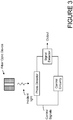
- the system includes a photo detector, control circuitry to generate control signals and apply such control signals to the photo detector, which, in response, detects light incident thereon, and a signal detector according to an aspect of the present invention.
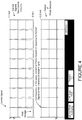
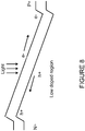
- FIGURE 4 illustrates the control signals and the response thereto by the photo detector (when light is incident thereon).
- the proximity sensor system may employ a laser or LED to generate a plurality of light pulses.
- the photo detector may be maintained in a non-detecting state and periodically placed in a detecting or sensing state/mode.
- the photo detector may be placed in a sensing state or mode via sense control pulses from the control circuitry. These control pulses may be synchronized with laser pulses.
- the photo detector When in the sensing state or mode, the photo detector is capable of detecting light reflected from the object onto the detector.
- the photo detector in response to the reflected light being incident thereon, generates an output signal (for example, an output current).
- the output signal is detected by a signal detector. As noted in the U.S.
- Patent Publication US 9,735,304 B1 this may be implemented via application of a reverse bias voltage is applied to the photo detector (i.e., no detection control signal applied to the photo detector).
- the photo detector is in a non-detection state via application of the hold voltage wherein charge carriers are "removed" from low-doped region.
- the hold voltage wherein charge carriers are "removed" from low-doped region.
- the triggering time of the photo detector may be less than 20 picoseconds.
- the present invention may employ any photo diode or detector to implement the present invention including the photo detector architectures described in U.S. Patent Application Publication US 2012/0313155 A1 .
- the photo detector includes at least one control node or gate (illustrated in the exemplary embodiment as Gate 1), a light absorbing region, a first doped region (illustrated in the exemplary embodiment as p+ region) and a second doped region (illustrated as contact region).
- the contact region is disposed and/or formed in the substrate region and on the major surface containing the p+ region(s) and the gates; and, in operation, may be an output of the photo detector.
- the contact region (regions) may be p+ or n+ region (regions).
- the photo detector may be fabricated in or on silicon, (for example, a standard bulk silicon), silicon-germanium, gallium-arsenide or an insulator (for example, glass or the like) or fabricated in or on a semiconductor-on-insulator (SOI) substrate (for example, a silicon or germanium region/layer/material disposed on or over an insulator region/layer/material (for example, a silicon oxide, silicon nitride and/or combination thereof).
- silicon for example, a standard bulk silicon
- silicon-germanium, gallium-arsenide or an insulator for example, glass or the like
- SOI semiconductor-on-insulator
- control nodes or gates may be comprised of a conductive type material (conductor or doped semiconductor), for example, a metal (for example, aluminum or copper), metal compound and/or a doped semiconductor (for example, silicon doped with donor or acceptor impurities).
- a conductive type material for example, a metal (for example, aluminum or copper), metal compound and/or a doped semiconductor (for example, silicon doped with donor or acceptor impurities).
- the gates are spaced from the body region via an insulator or dielectric material (for example, silicon oxide, silicon nitride or combinations or composites thereof, for example, ONO).
- the light absorbing region may be fabricated in or on the substrate.
- the body region is an intrinsic or doped semiconductor (for example, intrinsic/undoped silicon, germanium or silicon-carbide or a lightly doped (with donor or acceptor impurities) silicon, germanium or silicon-carbide).
- the light absorbing region may be one or more materials from the Group IV semiconductor including silicon, germanium, silicon carbide and/or combinations thereof (for example, silicon-germanium).
- the light absorbing region body may be an intrinsic material or a material having impurities, for example, n-type or p-type material(s).
- the photo detector includes at least one doped region - see, p+ regions.
- the doped semiconductor regions may be disposed and/or formed in or on the substrate.
- the p-type semiconductor material may be formed in the substrate by doping the semiconductor with a p-type impurity (for example, boron).
- the doped semiconductor regions (p+ regions) are also control nodes of the photo detector and, in operation, an output of the photo detector.
- the contact region is formed in the substrate region (for example, via conventional lithographic, etching and deposition techniques) and is comprised of a conductive type material (conductor or semiconductor), for example, a metal (for example, aluminum or copper), metal compound and/or a doped semiconductor (for example, silicon, silicon-germanium or gallium arsenide doped with donor or acceptor impurities).
- a conductive type material for example, a metal (for example, aluminum or copper), metal compound and/or a doped semiconductor (for example, silicon, silicon-germanium or gallium arsenide doped with donor or acceptor impurities).
- the contact region may be an acceptor type material such as p+ doped silicon, germanium, silicon-germanium, silicon-carbide or gallium arsenide.
- the contact region is a p+ type material consisting of one or more materials from the Group IV semiconductor including silicon, germanium, silicon carbide and/or combinations thereof.
- the contact region is formed from a portion of the substrate region.
- the substrate may be doped with acceptor type dopants forming, for example, p+ doped silicon, germanium, silicon-germanium, silicon-carbide or gallium arsenide.
- the dopant may be boron or aluminum to provide or incorporate atoms (acceptors) into a selected portion of the substrate region in order to increase the number of free charge carriers (in this case positive carriers or holes).
- the substrate region photo detector in the exemplary embodiment may be a semiconductor on insulator (SOI) substrate (for example, a silicon or germanium region/layer/material disposed on or over an insulator region/layer/material (for example, a silicon oxide, silicon nitride and/or combination thereof) or a silicon, (for example, a standard bulk silicon), silicon-germanium, gallium-arsenide and/or combination thereof.
- SOI semiconductor on insulator
- a negative voltage VC ⁇ 0V
- VG1 > 4V negative voltage
- VI +3V
- the electron barrier (band gap) is lowered therein. This results in an additional and/or greater hole current flow from the p+ regions through a portion of the substrate region to the contact region. That is, an additional and/or greater hole current is created and flows from the p+ regions through a portion of the body region and the light absorbing region to the p+ contact region thereby increasing the magnitude of the output current.
- the photo detector is in a conductive state or mode which provides a large internal current gain. The current flows between the p+ region and the contact region and an output current upon detecting or in response to the incident light.
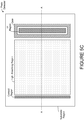
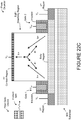
- FIGURES 5B and 5C illustrate exemplary top views of the cross-sectional views of the photo detectors of FIGURE 5A wherein dotted lines A-A in FIGURES 5B and 5C indicate the location of the cross-sectional views of FIGURE 5A .
- the contact regions of the exemplary embodiments of FIGURES 5A-5C have been described as a p+ region, in another embodiment, the contact region may be an n+ type.
- the circuitry and techniques of the present invention may maintain the photo detector in a non-detection state via application of a reverse bias voltage being applied to the photo detector (i.e., no detection control signal applied to the photo detector).
- the photo detector is in a non-detection state via application of the hold voltage wherein charge carriers are "removed" from low-doped region.
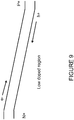
- the hold voltage is -5V. (See, FIGURES 4 and 6 ).
- the non-detection state little to no current flows through the photo detector regardless of the presence of incident light.
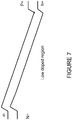
- the circuitry and techniques of the present invention may place the photo detector in a ready state via application of a detect voltage wherein potential barriers adjacent to the n+ and p+ regions block or prevent current flow (for example, significant current flow). (See, FIGURE 7 ).
- the detect voltage for example, +1V in this exemplary embodiment, places the photo detector in a forward bias state.
- the illustrated/exemplary voltage levels to implement or enable sensing by the photo detector are merely exemplary.
- the indicated voltage levels may be relative or absolute.
- the voltages indicated may be relative in that each voltage level, for example, may be increased or decreased by a given voltage amount (for example, each voltage may be increased or decreased by 0.1, 0.15, 0.25, 0.5, 1 volt) whether one or more of the voltages (for example, the voltages applied to n+ region and p+ region) become or are positive and negative.
- the detection time or triggering time of the photo detectors of the present invention may be programmable or tunable, for example, to meet or accommodate response time specifications as well as power consumption specification.
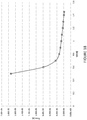
- the voltages applied to the n+ region and p+ region are adjusted to decrease the response time of the photo detector -- for example, by increasing the electric field within the body region.
- the electric field between the n+ region and p+ region and associated region is adjusted (for example, increased) to adjust the response time (for example, decrease) of the photo detector.
- the voltages applied to the n+ region and p+ region are adjusted to reduce the power consumption of the photo detector.
- the response time and/or power consumption may be controlled, adjusted and/or programmed to, for example, accommodate desired/required specifications of the photo detector.
- the photo detector is placed in a predetermined or non-detection state before sensing the light (or data) via application of a hold voltage.
- carriers may be removed from the low-doped region prior to sensing so that the concentration of carriers in that region at the initiation of sensing is below a predetermined value.
- the photo detector is placed in a predetermined or non-detection state by applying a reverse bias voltage to the first and second doped regions to remove carriers from the body region. Establishing the photo detector in a predetermined or non-detection state (for example, periodically) before sensing may enhance or increase the stability and/or accuracy of the photo detector during sensing.
- the photo detector includes at least two doped regions - a p+ region and an n+ region.
- the doped semiconductor regions may be disposed and/or formed in or on the substrate and juxtaposed the low doped region.
- the p-type semiconductor material may be formed in the substrate by doping the semiconductor with a p-type impurity (for example, boron).
- the low-doped region may be fabricated in or on the substrate.
- the body region is an intrinsic or doped semiconductor (for example, intrinsic/undoped silicon, germanium or silicon-carbide or a lightly doped (with donor or acceptor impurities) silicon, germanium or silicon-carbide).
- the low-doped region may be one or more materials from the Group IV semiconductor including silicon, germanium, silicon carbide and/or combinations thereof (for example, silicon-germanium).
- the low-doped region may be an intrinsic material or a material having impurities, for example, n-type or p-type material(s).
- the photo detectors of the present invention may be implemented in a discrete device (for example, discrete photon receiver element) as well as in conjunction with any type of integrated circuitry (for example, integrated CMOS photon receiver circuitry).
- a discrete device for example, discrete photon receiver element
- integrated circuitry for example, integrated CMOS photon receiver circuitry
- the present invention relates to an array of photo detectors according to any of the embodiments described and/or illustrated herein.
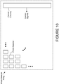
- the array may include, in addition to the array of photo detectors, control circuitry to manage the acquisition, capture and/or sensing operations of the photo detectors of the array. (See, for example, FIGURE 10 ).
- the control circuitry may control or enable/disable the photo detectors in a manner so that data acquisition or sensing correlates to the data rate of the transmission.
- the photo detector array is coupled to a plurality of fiber optic output devices wherein each fiber optic device is associated with one or more photo detectors of the array and the control circuitry may control or enable/disable the subset of photo detectors in accordance with the associated output of the fiber optic device.
- the photo detector array may be formed from a plurality of discrete devices and/or from a plurality of photo detectors integrated on a die wherein the photo detector array portion includes a plurality of photo detectors to acquire, capture, convert and/or sense the incident light from one or more associated fiber optic output(s).
- the photo detectors may be configured and/or arranged in any array architecture as well as in conjunction with any type of integrated circuitry.
- the present invention may be implemented in high-speed data transmission that employs photon data transmission (for example, via a fiber optic).
- the photo detector may be coupled to a signal detector (current detector and/or other circuitry) to measure/condition the current output by the photo detector (for example, output via the p+ and n+ doped regions in response to the detection of light/data in the exemplary embodiments illustrated in FIGURES 3 , 4 , 10 and 11 ).
- the current photo detector may be a high-speed current detector or the like.
- the p+ and n+ regions in the embodiments described and/or illustrated herein may be formed by or in a semiconductor (for example, silicon doped with acceptor/donor impurities).
- the photo detector, photo detector array and/or die/device may include an anti-reflective material disposed there over or thereon.
- an anti-reflective material is disposed over or on the light absorbing region of the photo detector or photo detectors (of the array of photo detectors).
- an anti-reflective material may be disposed on or over the entire structure, or a significant portion thereof.
- the present invention may be implemented in a discrete photo detector or in an integrated circuit device having a photon receiver section (which may include one or more photo detectors (including an array of photo detectors)).
- the photo detectors of the present invention may be implemented in the standard planar technology (as illustrated herein) or any 3D technology (for example, planar or vertical type), or pillar architectures).
- the body region of the photo detector may or may not be electrically floating in view of the insulation or non-conductive region (for example, in bulk-type material/substrate).
- the photo detector may be formed on an SOI substrate or bulk silicon substrate.
- the present invention may employ any photo diodes or photo detectors to implement the present invention, including the photo diode or photo detector layouts/architectures described in U.S. Patent Application Publication US 2012/0313155 A1 .
- Exemplary photo detector layouts/architectures are discussed above and illustrated in FIGURES 5A-5C .
- Other photo detector layouts/architectures are discussed immediately below.
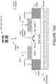
- a photo detector includes at least two control nodes or gates (illustrated in the exemplary embodiment as Gate 1 and Gate 2), a light absorbing region, a body region, a first doped region (illustrated in the exemplary embodiment as n+ region) and a second doped region (illustrated in the exemplary embodiment as p+ region).
- the photo detector in this exemplary embodiment, is fabricated in or on a semiconductor on insulator (SOI) substrate (for example, a silicon or germanium region/layer/material disposed on or over an insulator region/layer/material (for example, a silicon oxide, silicon nitride and/or combination thereof).
- SOI semiconductor on insulator
- control nodes or gates may be comprised of a conductive type material (conductor or semiconductor), for example, a metal (for example, aluminum or copper), metal compound and/or a doped semiconductor (for example, silicon doped with donor or acceptor impurities).
- a conductive type material for example, a metal (for example, aluminum or copper), metal compound and/or a doped semiconductor (for example, silicon doped with donor or acceptor impurities).
- the gates are spaced from the body region via an insulator or dielectric material (for example, silicon oxide, silicon nitride or combinations or composites thereof, for example, ONO).
- the body region may be an intrinsic or doped semiconductor (for example, intrinsic/undoped silicon or germanium or a lightly doped (with donor or acceptor impurities) silicon or germanium) including an intrinsic material or a material having impurities, for example, n-type or p-type materials.
- the body region may be one or more materials from the Group IV semiconductor including silicon, germanium, silicon carbide and/or combinations thereof.
- the photo detector according to this embodiment includes at least two doped semiconductor regions including n+ and p+ regions. These doped semiconductor regions may be formed within a semiconductor layer consisting of the body region.
- the n-type semiconductor material may be formed from or by doping such semiconductor layer (for example, silicon layer) with an n-type impurity (for example, phosphorus or arsenic).
- the p-type semiconductor material may be formed from or by doping such semiconductor with a p-type impurity (for example, boron).
- the doped semiconductor regions (n+ and p+ regions) are outputs of the photo detector.
- the photo detector is enabled to detect incident light via application of selected or predetermined voltages to the gates and the doped regions (here, n+ and p+ regions).
- a negative voltage applied to Gate 1 for example, -2V
- a negative or zero voltage is applied to the n+ region
- a positive voltage applied to Gate 2 for example, 2V
- a positive voltage for example, 1V
- the applied or incident light generates electron-hole pairs in the body region of the photo detector -- where the electrons and holes of such pairs are separated by an electric field within the body region.
- the voltages for example, static or fixed voltages
- the gates, n+ and p+ regions create or provide the electric field within the body region.
- positive carriers i.e., holes
- negative carriers i.e., electrons
- the excess of holes in the region 1 will induce a lowering of the barrier to electron movement (band gap) and electron current flow from n+ region.
- excess of electrons in the region 2 provides, induces or causes a lowering of the hole barrier and hole current flowing from p+ region.
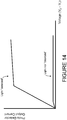
- a positive feedback mechanism accelerates accumulation of excess carriers under the respective gates, which, in turn, reduce the potential barriers related corresponding to such regions and causes a current to flow between the p+ and n+ regions of the photo detector and an output current upon detecting or in response to the incident light. (See, for example, FIGURE 14 ).
- the photo detector may be disabled via removing/changing the voltages applied to one or more of Gate 1, n+ region, p+ region and/or Gate 2, and/or applying opposite polarity voltages to one or more of Gate 1, n+ region, p+ region and/or Gate 2. For example, increasing the amplitude on one or both of the voltages applied to the gates may place the sensor in a non-conductive state.
- the illustrated/exemplary voltage levels to implement or enable sensing by the photo detector are merely exemplary.
- the indicated voltage levels may be relative or absolute.
- the voltages indicated may be relative in that each voltage level, for example, may be increased or decreased by a given voltage amount (for example, each voltage may be increased or decreased by 0.1, 0.15, 0.25, 0.5, 1 volt) whether one or more of the voltages (for example, the voltages applied to Gate 1, n+ region, p+ region and/or Gate 2) become or are positive and negative.
- the detection time or triggering time of the photo detectors may be programmable or tunable, for example, to meet or accommodate response time specifications as well as power consumption specification.
- the voltages applied to the gates are adjusted to increase the response time of the photo detector -- for example, by increasing the electric field within the body region.
- the electric field between the gate and associated region is adjusted (for example, increased) to adjust the response time (for example, increase) of the photo detector.
- the voltages applied to the gates are adjusted to reduce the power consumption of the photo detector.
- the response time and/or power consumption may be controlled, adjusted and/or programmed to, for example, accommodate desired/required specifications of the photo detector.
- the photo detector is placed in a predetermined state before sensing the light (or data).
- carriers may be removed from the body region prior to sensing so that the concentration of carriers in the body region (and beneath the gates (Regions 1 and 2)) at the initiation of sensing is below a predetermined value.
- the photo detector includes a carrier generation region (CG region) in addition to at least two control nodes or gates (illustrated in the exemplary embodiment as Gate 1 and Gate 2), a light absorbing region, a body region, a first doped region (illustrated in the exemplary embodiment as n+ region) and a second doped region (illustrated in the exemplary embodiment as p+ region).
- the CG region may include a material which facilitates greater/higher generation of carriers in response to incident light. That is, in one embodiment, the CG region includes a material which generates more electron-hole carriers, relative to the embodiment illustrated in FIGURE 12A , in response to incident light.
- the CG region includes germanium, gallium-arsenide or silicon-germanium, or combinations thereof (for example, both germanium and gallium-arsenide).
- the CG region may also include a highly doped semiconductor material (for example, highly doped silicon) which is more responsive to photons than a similar undoped or a lightly doped semiconductor material.
- the CG region in this embodiment facilitates greater/higher generation of carriers in response to incident light having the same or lower photon energy.
- the photo detector of FIGURE 15A may detect light (photon transmission) having a lower energy in connection with the transmission thereof.
- the CG region includes a material that is less responsive to photon energy.
- the CG region includes a material which generates fewer electron-hole carriers, relative to the embodiment illustrated in FIGURE 12A , in response to incident light.
- the CG region includes amorphous silicon or lightly doped polycrystalline silicon. The photo detector of this embodiment may be less susceptible to noise that may be present on or in the incident light (data).
- FIGURES 15B and 15C illustrate exemplary top views of the cross-sectional views of the photo detectors of FIGURE 15A wherein dotted lines A-A indicate the location of the cross-sectional views of FIGURES 15B and 15C .
- gates 1 and 2 are interconnected as one structure.
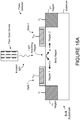
- the photo detector may be fabricated on or in a bulk wafer/substrate.
- a photo detector according to this embodiment includes at least two control nodes or gates (illustrated in the exemplary embodiment as Gate 1 and Gate 2), a light absorbing region, a body region, a first doped region (illustrated in the exemplary embodiment as n+ region) and a second doped region (illustrated in the exemplary embodiment as p+ region).
- the photo detector in this exemplary embodiment, is fabricated in or on a bulk semiconductor wafer/substrate (for example, undoped or lightly doped silicon, germanium, or gallium arsenide.
- the low or lightly doped silicon substrate may "appear" as a dielectric in those instances where the photo detector device operates at high frequencies.
- a significant majority of the carriers are maintained in a region of the body near the surface of the device closest to the incident light. In this way, a current is formed between the n+ and p+ regions in the body region immediately below the gates.
- the detection time or triggering time of the exemplary photo detectors of FIGURES 16A and 16B may be programmable or tunable, for example, to meet or accommodate response time specifications as well as power consumption specification.
- the voltages applied to the gates are adjusted to increase the response time of the photo detector (for example, by increasing the electric field).
- the voltages applied to the gates are adjusted to reduce the power consumption of the photo detector.
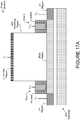
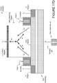
- a photo detector includes at least one control node or gate (the exemplary cross-sectional view of the photo detector of FIGURES 17A and 17B illustrates two control nodes or gates - see, Gate 1 and Gate 2), a light absorbing region, a body region, and at least one doped impurity region (the exemplary embodiment of FIGURES 17A and 17B again illustrate two doped regions - see p+ regions) which is disposed in a positional relationship to one or more control nodes or gates.
- the photo detector also includes a contact region which, in operation, is an output of the photo detector.
- the photo detector in the exemplary embodiment of FIGURE 17A is fabricated in or on a semiconductor on insulator (SOI) substrate (for example, a silicon or germanium region/layer/material disposed on or over an insulator region/layer/material (for example, a silicon oxide, silicon nitride and/or combination thereof).
- SOI semiconductor on insulator
- the photo detector in the exemplary embodiment of FIGURE 17B may be fabricated on silicon, (for example, a standard bulk silicon), silicon-germanium, gallium-arsenide or an insulator (for example, glass or the like).
- control nodes or gates may be comprised of a conductive type material (conductor or doped semiconductor), for example, a metal (for example, aluminum or copper), metal compound and/or a doped semiconductor (for example, silicon doped with donor or acceptor impurities).
- a conductive type material for example, a metal (for example, aluminum or copper), metal compound and/or a doped semiconductor (for example, silicon doped with donor or acceptor impurities).
- the gates are spaced from the body region via an insulator or dielectric material (for example, silicon oxide, silicon nitride or combinations or composites thereof, for example, ONO).
- the body region may be fabricated in or on the substrate.
- the body region is an intrinsic or doped semiconductor (for example, intrinsic/undoped silicon, germanium or silicon-carbide or a lightly doped (with donor or acceptor impurities) silicon, germanium or silicon-carbide).
- the body region may be one or more materials from the Group IV semiconductor including silicon, germanium, silicon carbide and/or combinations thereof (for example, silicon-germanium).
- the body may be an intrinsic material or a material having impurities, for example, n-type or p-type material(s).
- the photo detector includes at least one doped region - see, p+ regions.
- the doped semiconductor regions may be disposed and/or formed in or on the substrate and juxtaposed the body region.
- the p-type semiconductor material may be formed in the substrate by doping the semiconductor with a p-type impurity (for example, boron).
- the doped semiconductor regions (p+ regions) are also control nodes of the photo detector and, in operation, an output of the photo detector.
- the light absorbing region in one embodiment, is disposed and/or formed on the substrate and may be comprised of a material having a high electron mobility, for example, germanium, silicon-germanium or gallium arsenide. In this way, in operation, electrons which are displaced from certain orbitals, in response to impinging light or photons, may more readily or easily move within the light absorbing region.
- the contact region is disposed and/or formed on or in the contact region and may be comprised of a conductive type material (conductor or semiconductor), for example, a metal (for example, aluminum or copper), metal compound and/or a doped semiconductor (for example, silicon, silicon-germanium or gallium arsenide doped with donor or acceptor impurities).
- the contact region is an acceptor type material such as p-type semiconductor material formed from or by doping a semiconductor with a p-type impurity (for example, boron, germanium, silicon-germanium, silicon-carbide or gallium arsenide.
- the contact region is a p+ type material consisting of one or more materials from the Group IV semiconductor including silicon, germanium, silicon carbide and/or combinations thereof.
- the photo detector detects incident light via application of selected or predetermined voltages to the gates, the doped regions (in this illustrated embodiment, p+ regions) and contact region (in this embodiment, a p+ contact region).
- the photo detector is essentially in a nonconductive state wherein a current between the contact region and the p+ regions is quite small.
- the photo detector in response to light incident on or applied to the light absorbing region of the photo detector (for example, light which is output from a fiber optic device), electron-hole pairs are generated in the light absorbing region (for example, germanium or silicon-germanium).
- the electron-hole pairs separate, in the presence of the electric field produced or provided by the voltages (for example, static or fixed voltages) applied to the gates, p+ regions and the p+ contact region.
- the voltages for example, static or fixed voltages
- holes are attracted to and flow to the p+ contact region and electrons are attracted to and flow to the body region and, in particular, to the body region near and/or beneath the gates (i.e., gate 1 and gate 2).
- the electron-hole pairs are separated by an electric field and the holes flow to the p+ contact region and the electrons flow to portions of the body region near and/or beneath the gates.
- This induces or causes the potential barrier lowering for holes in the body region located near and/or beneath the gates as excess electrons accumulate in that region.
- an additional and/or greater hole current is created and flows from the p+ regions through a portion of the body region and the light absorbing region to the p+ contact region thereby increasing the magnitude of the output current.
- negative carriers i.e., electrons
- positive carriers i.e., holes
- the photo detector is in a conductive state or mode, which provides a large internal current gain.
- the current flows between the p+ regions and the contact region and an output current upon detecting or in response to the incident light.
- little to no current flows between the p+ regions and the contact region due to the barrier caused or provided by the voltages applied to the gates.
- the photo detector may be disabled via removing/changing the voltages applied to one or more of Gates 1 and 2, contact region, p+ regions, and/or applying voltages of opposite polarity to one or more of one or more of Gates 1 and 2, contact region, p+ regions. For example, decreasing the voltages applied to the gates and/or p+ regions may place the photo detector in a non-conductive state.
- the illustrated/exemplary voltage levels to implement or enable sensing by the photo detector are merely exemplary.
- the indicated voltage levels may be relative or absolute.
- the voltages indicated may be relative in that each voltage level, for example, may be increased or decreased by a given voltage amount (for example, each voltage may be increased or decreased by 0.1, 0.15, 0.25, 0.5, 1 volt) whether one or more of the voltages (for example, the voltages applied to Gates 1 and 2, p+ regions and/or contact region become or are positive and negative.
- the detection time of the photo detectors may be programmable or tunable, for example, to meet or accommodate response time specifications as well as power consumption specification.
- the voltages applied to the gates are adjusted to increase the response time of the photo detector (for example, by increasing the electric field).
- the voltages applied to the gates are adjusted to reduce the power consumption of the photo detector.
- the response time and/or power consumption may be adjusted, for example, to accommodate desired/required specifications.
- the voltages applied to the n+ region and p+ region are adjusted to decrease the response time of the photo detector -- for example, by increasing the electric field within the body region.
- the electric field between the n+ region and p+ region and associated region is adjusted (for example, increased) to adjust the response time (for example, decrease) of the photo detector.
- the voltages applied to the n+ region and p+ region are adjusted to reduce the power consumption of the photo detector.
- FIGURE 18 shows an exemplary embodiment of the effect of increase of electric field applied to the n+ and p+ regions on the response time of the photo detector.
- the response time and/or power consumption may be controlled, adjusted and/or programmed to, for example, accommodate desired/required specifications of the photo detector.
- the photo detector is placed in a predetermined state before sensing the light (or data).
- carriers may be removed from the body region prior to sensing so that the concentration of carriers in the body region (and near and/or beneath the gates) at the initiation of sensing is below a predetermined value.
- the photo detector is placed in a predetermined state by applying predetermined voltages to the p+ regions and applying voltage pulses to the gates to remove carriers from the body region thereby providing depletion regions under gates Gate 1 and Gate 2. Establishing the photo detector in a predetermined state (for example, periodically) before sensing may increase or enhance the stability, response time and/or accuracy of the photo detector during sensing/operation.
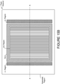
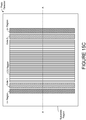
- FIGURES 19A-19C illustrate exemplary top views of the cross-sectional views of the photo detectors of FIGURES 17A-17C wherein dotted lines A-A indicate the location of the cross-sectional views of FIGURES 17A-17C .
- the gates 1 and 2 are interconnected as one structure.
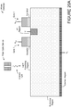
- the photo detector includes a contact region disposed on a backside surface of the substrate region (for example, the major surface which is opposing the major surface upon which the p+ region and gates are disposed).
- the primary light absorbing region is a portion of the substrate region which, in an exemplary embodiment, may be silicon (for example, a low doped p-type silicon substrate), silicon-germanium or gallium-arsenide or combinations thereof (for example, both germanium and gallium-arsenide).
- the light absorbing region is a material which facilitates generation of carriers in response to incident light.
- the light absorbing region may be a doped or undoped material (for example, a highly doped semiconductor material (for example, highly doped silicon) which is more responsive to photons than a similar undoped or a lightly doped semiconductor material).
- the contact region is a p+ type contact region.
- the holes flow to the p+ contact region and electrons flow to the body region and, in particular, to the body region near and/or beneath the gates (i.e., Gate 1).
- the electron barrier (band gap) is lowered therein. This results in an additional and/or greater hole current flow from the p+ regions through a portion of the substrate region to the contact region.
- the operation of the photo detector of FIGURE 20A is substantially the same as described above with respect to the photo detector of FIGURES 17A and 17B . For the sake of brevity, that discussion will not be repeated.
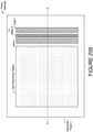
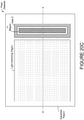
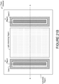
- FIGURES 20B and 20C illustrate exemplary top views of the cross-sectional views of the photo detectors of FIGURE 20A wherein dotted lines A-A indicate the location of the cross-sectional views of FIGURE 20A .
- the exemplary photo detector of FIGURE 20A may include two or more p+ region, each p+ region having associated gates.
- the photo detector includes at least two doped regions (p+ regions) each having a positional relationship to associated gates or control nodes - namely, gate 1 and gate 2, respectively.
- the materials and configuration of the gates and the doped region (p+ region) may be the same as that described in connection with the embodiment of FIGURES 17A , 17B and 20A . For the sake of brevity, that discussion will not be repeated.
- the operation of the photo detector of FIGURE 21A is substantially the same as described above with respect to the photo detector of FIGURES 20A . That is, in response to incident light, electrons and holes are created in the light absorbing region and are separated in the presence of an electric field produced or provided by the voltages (for example, static or fixed voltages) applied to the p+ region (for example, +3V), gates (for example, greater than +4V) and the contact region (a negative or ground voltage). As excess electrons accumulate in the substrate region located near and/or beneath the gates, the potential barrier for holes lowers in that region thereby providing for a hole current which flows from the p+ regions to the contact region.
- the contact region is again a p+ type contact region.
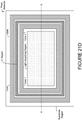
- FIGURES 21B and 21C illustrate exemplary top views of the cross-sectional views of the photo detectors of FIGURE 21A wherein dotted lines A-A in FIGURES 21B and 21C indicate the location of the cross-sectional views of FIGURE 21A .
- gates 1 and 2 may be interconnected as one structure.
- the exemplary photo detector illustrated in FIGURE 21A may generate a larger current in response to incident light. That is, the plurality of p+ regions (having associated gates juxtaposed thereto) may in combination generate a larger current in response to incident light.
- the photo detector embodiment of FIGURE 21A may be employed as a "building block" of an array of photo detectors of a photo detector device wherein the gates are electrically connected and the outputs are connected in parallel. Indeed, all of the embodiments herein may be employed as "building blocks" of an array of photo detectors of a photo detector device.
- substrate is low doped and an electric field exists in the region between the contact region and the p+ regions.
- the contact region of the aforementioned embodiments have often been described as a p+ region, in another embodiment, the contact region may be an n+ type.
- the photo detector may be characterized as an n+pnp+ type structure.
- the materials, architecture and layout of the photo detector may be the same except for the n+ contact region. Accordingly, the discussion above in connection with FIGURES 17A and 17B (for example, the materials) are applicable to this embodiment and, for the sake of brevity will not be repeated.
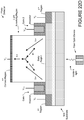
- the electron-hole pairs are separated by an electric field and the holes flow to the n+ contact region and the electrons flow to portions of the body region near and/or beneath the gates.
- the potential barrier for holes lowers in the body region located near and/or beneath the gates providing for an additional and/or greater hole current to flow from the p+ regions to the contact region thereby increasing the magnitude of the output current.
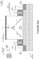
- the photo detectors of FIGURES 22A-22D in a conductive state or mode, provides a large internal current gain due to a positive feedback mechanism of accumulation of excess negative carriers under the gates, which, in turn, reduces the band gaps corresponding to such regions.
- the current flows between the p+ regions and the n+ contact region and an output current upon detecting or in response to the incident light.
- the detection time or triggering time of the exemplary photo detectors may be programmable or tunable, for example, to meet or accommodate response time specifications as well as power consumption specification.
- the voltages applied to the gates are adjusted to increase the response time of the photo detector (for example, by increasing the electric field).
- the voltages applied to the gates are decreased to reduce the power consumption of the photo detector.
- the photo detectors may be implemented in a discrete device (for example, discrete photon receiver element) as well as in conjunction with any type of integrated circuitry (for example, integrated CMOS photon receiver circuitry).
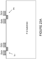
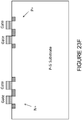
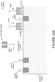
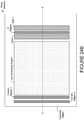
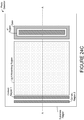
- the photo detectors may be fabricated via a CMOS process. (See, for example, FIGURES 23A-23F ).
- the p+ regions, gates and contact regions may be fabricated during or in relation to the CMOS process of fabricating the PMOS and NMOS transistors.
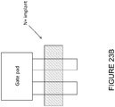
- an n+ implant may be performed (see FIGURE 23B ), and thereafter a contact to a portion of the n+ region may be formed (see FIGURE 23C ).
- FIGURE 23F illustrates a cross-section of the resulting or "final" structure.
- the photo detector does not include n+ regions as in several of the exemplary embodiments set forth herein, the n+ processing in connection with the photo detector may be omitted.
- the n+ and p+ implantations of the photo detector may be performed during formation of the CMOS transistors. Alternatively, the n+ and p+ implantations of the photo detector may be performed before or after formation of the CMOS transistors. Moreover, the light absorbing regions and contact regions of the photo detectors of FIGURES 12A , 15A , 16A , 16B , 17A and 22A may be fabricated after such CMOS process without impact to the CMOS circuitry.
- the photo detectors may be configured and/or disposed as an array according to any of the embodiments described and/or illustrated herein.
- the array may include, in addition to the array of photo detectors, control circuitry to manage the acquisition, capture and/or sensing operations of the photo detectors of the array. (See, for example, FIGURE 10 ).
- the control circuitry may control or enable/disable the photo detectors in a manner so that data acquisition or sensing correlates to the data rate of the transmission.
- the photo detector array is coupled to a plurality of fiber optic output devices wherein each fiber optic device is associated with one or more photo detectors of the array and the control circuitry may control or enable/disable the subset of photo detectors in accordance with the associated output of the fiber optic device.
- the photo detector array may be formed from a plurality of discrete devices and/or from a plurality of photo detectors integrated on a die wherein the photo detector array portion includes a plurality of photo detectors to acquire, capture, convert and/or sense the incident light from one or more associated fiber optic output(s).
- the photo detectors may be configured and/or arranged in any array architecture as well as in conjunction with any type of integrated circuitry.
- the photo detector(s) may be coupled to a current amplifier or photo detector (and other circuitry) to measure/condition the current output by the photo detector (for example, output via the contact region and p+ doped regions in response to the detection of light/data in the exemplary embodiments illustrated in FIGURES 5A , 17A , 17B , 20A , 20B , 22A and 22B ).
- the current photo detector may be a high-speed sense amplifier or the like.
- the gates, contact region and p+ regions in the embodiments described and/or illustrated herein may be formed by or in a semiconductor (for example, silicon doped with acceptor impurities).
- a semiconductor for example, silicon doped with acceptor impurities.
- one or more (or all) of such features (gates and regions) may be comprised of or formed (whether wholly or partially) from a metal (for example, aluminum or copper) or metal compound.
- the photo detector, photo detector array and/or die/device may include an anti-reflective material disposed there over or thereon.
- an anti-reflective material is disposed over or on the light absorbing region of the photo detector or photo detectors (of the array of photo detectors).
- an anti-reflective material may be disposed on or over the entire structure, or a significant portion thereof.
- the photo detectors may be implemented in a discrete photo detector or in an integrated circuit device having a photon receiver section (which may include one or more photo detectors (including an array of photo detectors)). Moreover, the photo detectors may be implemented in the standard planar technology (as illustrated herein) or any 3D technology (for example, planar or vertical type), or pillar gate architectures). The body region of the photo detector may or may not be electrically floating in view of the insulation or non-conductive region (for example, in bulk-type material/substrate). As illustrated herein, the photo detector may be formed on an SOI substrate or bulk silicon substrate.
- photo detectors employed in the present invention may include one or more additional contact regions (n+ or p+ type contact regions).
- the exemplary photo detector includes an additional contact region (contact region 2) to improve the performance of the detector.
- the illustrated/exemplary voltage levels to implement or enable sensing by the photo detector are merely exemplary.
- the indicated voltage levels may be relative or absolute.
- the voltages indicated may be relative in that each voltage level, for example, may be increased or decreased by a given voltage amount (for example, each voltage may be increased or decreased by 0.1, 0.15, 0.25, 0.5, 1 volt) whether one or more of the voltages.
- circuit may mean, among other things, a single component or a multiplicity of components (whether in integrated circuit form or otherwise), which are active and/or passive, and which are coupled together to provide or perform a desired function.
- circuitry may mean, among other things, a circuit (whether integrated or otherwise), a group of such circuits, one or more processors, one or more state machines, one or more processors implementing software, one or more gate arrays, programmable gate arrays and/or field programmable gate arrays, or a combination of one or more circuits (whether integrated or otherwise), one or more state machines, one or more processors, one or more processors implementing software, one or more gate arrays, programmable gate arrays and/or field programmable gate arrays.
- data may mean, among other things, a current or voltage signal(s) whether in an analog or a digital form, which may be a single bit (or the like) or multiple bits (or the like).
- references herein to "one embodiment” or “an embodiment” herein means that a particular feature, structure, or characteristic described in connection with the embodiment can be included in one some or all of the embodiments of the present invention.
- the usages or appearances of the phrase “in one embodiment” or “in another embodiment” in the specification are not referring to the same embodiment, nor are separate or alternative embodiments necessarily mutually exclusive of one or more other embodiments. The same applies to the term “implementation.”
- circuits and circuitry disclosed herein may be described using computer aided design tools and expressed (or represented), as data and/or instructions embodied in various computer-readable media, for example, in terms of their behavioral, register transfer, logic component, transistor, layout geometries, and/or other characteristics.
- Formats of files and other objects in which such circuit expressions may be implemented include, but are not limited to, formats supporting behavioral languages such as C, Verilog, and HLDL, formats supporting register level description languages like RTL, and formats supporting geometry description languages such as GDSII, GDSIII, GDSIV, CIF, MEBES and any other suitable formats and languages.
- Computer-readable media in which such formatted data and/or instructions may be embodied include, but are not limited to, nonvolatile storage media in various forms (e.g., optical, magnetic or semiconductor storage media) and carrier waves that may be used to transfer such formatted data and/or instructions through wireless, optical, or wired signaling media or any combination thereof.
- Examples of transfers of such formatted data and/or instructions by carrier waves include, but are not limited to, transfers (uploads, downloads, e-mail, etc.) over the Internet and/or other computer networks via one or more data transfer protocols (e.g., HTTP, FTP, SMTP, etc.).
- Such data and/or instruction-based expressions of the above described circuits may be processed by a processing entity (e.g., one or more processors) within the computer system in conjunction with execution of one or more other computer programs including, without limitation, net-list generation programs, place and route programs and the like, to generate a representation or image of a physical manifestation of such circuits.
- a processing entity e.g., one or more processors
- Such representation or image may thereafter be used in device fabrication, for example, by enabling generation of one or more masks that are used to form various components of the circuits in a device fabrication process.
- circuits and circuitry, as well as techniques, disclosed herein may be represented via simulations and simulation instruction-based expressions using computer aided design, simulation and/or testing tools.
- the simulation of the circuitry of the present invention including the photo detector and/or techniques implemented thereby, may be implemented by a computer system wherein characteristics and operations of such circuitry, and techniques implemented thereby, are simulated, imitated, replicated, analyzed and/or predicted via a computer system.
- the present invention is also directed to such simulations and testing of the inventive device and/or circuitry, and/or techniques implemented thereby.
- the contact region of the photo detector may be disposed and/or formed in the substrate (see, for example, one of the p+ or n+ regions illustrated in the embodiment of FIGURES 12A , 15A , 16A and 16B ) or disposed and/or formed on the substrate (see, for example, the p+ contact region of the embodiments of FIGURES 17A-17E or the n+ contact region of the embodiments of FIGURES 22A-22D ).
- the term “determine” and “calculate” and other forms thereof means, among other things, calculate, assesses, determine and/or estimate and other forms thereof.
- data may mean, among other things, a current or voltage signal(s) whether in analog or a digital form (which may be a single bit (or the like) or multiple bits (or the like)).
- the terms “comprises,” “comprising,” “includes,” “including,” “have,” and “having” or any other variation thereof, are intended to cover a non-exclusive inclusion, such that a process, method, article, or apparatus that comprises a list of elements does not include only those elements but may include other elements not expressly listed or inherent to such process, method, article, or apparatus.
- circuits, circuitry, nodes and/or components are “coupled” means that the circuits, circuitry, nodes and/or components are joined and/or operate (for example, physically or electrically) together either directly or indirectly, i.e., through one or more intermediate circuits, circuitry, nodes and/or components, so long as a link occurs; "directly coupled” means that two elements are directly joined, in contact and/or operate with each other.
Landscapes
- Engineering & Computer Science (AREA)
- Physics & Mathematics (AREA)
- General Physics & Mathematics (AREA)
- Computer Networks & Wireless Communication (AREA)
- Radar, Positioning & Navigation (AREA)
- Remote Sensing (AREA)
- Electromagnetism (AREA)
- Spectroscopy & Molecular Physics (AREA)
- Light Receiving Elements (AREA)
- Optical Radar Systems And Details Thereof (AREA)
- Geophysics And Detection Of Objects (AREA)
- Photo Coupler, Interrupter, Optical-To-Optical Conversion Devices (AREA)
- Length Measuring Devices By Optical Means (AREA)
Claims (16)
- Système de capteur de proximité comprenant :un photodétecteur comprenant une première région dopée, une grille, une deuxième région dopée et une région absorbant la lumière, la région absorbant la lumière comportant au moins un matériau dans lequel, en réponse à de la lumière incidente sur celui-ci, des paires de porteurs de charge opposée sont générées, la première région dopée attirant un premier porteur des paires de porteurs ayant une première charge, la deuxième région dopée attirant un deuxième porteur des paires de porteurs ayant une deuxième charge, opposée, et le photodétecteur générant un signal de sortie révélateur de la présence d'un objet à proximité du système de capteur de proximité ;un circuit de commande destiné à générer une pluralité de signaux de commande devant être appliqués au photodétecteur, la pluralité de signaux de commande comprenant un premier signal de commande appliqué à la première région dopée du photodétecteur, un deuxième signal de commande appliqué à la grille du photodétecteur, et un troisième signal de commande appliqué à la deuxième région dopée du photodétecteur, les signaux de commande appliqués contrôlant un état de fonctionnement du photodétecteur ; etun détecteur de signal pour détecter le signal de sortie du photodétecteur ;caractérisé en ce que le circuit de commande est configuré pour placer le photodétecteur dans un état de détection en générant un deuxième ensemble d'amplitudes de tension relative pour les premier, deuxième et troisième signaux de commande de telle sorte que le photodétecteur est dans un mode de polarisation directe.
- Système de capteur de proximité de la revendication 1, dans lequel la première région dopée du photodétecteur est constituée d'un semi-conducteur de type p et la deuxième région dopée est constituée d'un semi-conducteur de type n.
- Système de capteur de proximité de la revendication 1, dans lequel le circuit de commande place le photodétecteur dans un état de non-détection en générant un premier ensemble d'amplitudes de tension relative pour les premier, deuxième et troisième signaux de commande de telle sorte que le photodétecteur est dans un mode de polarisation inverse avec sensiblement pas de circulation de courant dans le photodétecteur.
- Système de capteur de proximité de la revendication 3, dans lequel la première amplitude de tension appliquée à la première région dopée est inférieure à la troisième amplitude de tension appliquée à la deuxième région dopée.
- Système de capteur de proximité de la revendication 1, dans lequel il n'y a sensiblement pas de circulation de courant dans le photodétecteur en l'absence de lumière incidente sur le photodétecteur.
- Système de capteur de proximité de la revendication 5, dans lequel la première amplitude de tension appliquée à la première région dopée diffère de la troisième amplitude de tension appliquée à la deuxième région dopée d'environ 1 volt.
- Système de capteur de proximité de la revendication 1, dans lequel il y a circulation de courant dans le photodétecteur en présence de lumière incidente sur le photodétecteur.
- Système de capteur de proximité de la revendication 7, dans lequel l'augmentation d'un champ électrique entre les première et deuxième régions dopées réduit un temps pour la circulation de courant dans le photodétecteur en réponse à la lumière incidente.
- Système de capteur de proximité de la revendication 7, dans lequel la diminution d'un champ électrique entre les première et deuxième régions dopées augmente un temps pour la circulation de courant dans le photodétecteur en réponse à la lumière incidente.
- Système de capteur de proximité de la revendication 1, dans lequel le circuit de commande applique les signaux de commande pour faire alterner le photodétecteur entre un état de non-détection et un état de détection.
- Système de capteur de proximité de la revendication 10, dans lequel le circuit de commande place le photodétecteur dans l'état de non-détection en générant un premier ensemble d'amplitudes de tension relative des premier, deuxième et troisième signaux de commande de telle sorte que le photodétecteur est dans un mode de polarisation inverse avec sensiblement pas de circulation de courant.
- Système de capteur de proximité de la revendication 11, dans lequel le circuit de commande place le photodétecteur dans l'état de détection en générant un deuxième ensemble d'amplitudes de tension relative des premier, deuxième et troisième signaux de commande de telle sorte que le photodétecteur est dans un mode de polarisation directe avec sensiblement pas de circulation de courant en l'absence de lumière incidente et avec circulation de courant en présence de lumière incidente.
- Système de capteur de proximité de la revendication 1, comportant en outre une source de lumière puisée.
- Système de capteur de proximité de la revendication 13, dans lequel les impulsions de la source de lumière sont synchronisées avec le photodétecteur et émettent de la lumière quand le photodétecteur est dans un état de détection.
- Procédé de détection d'une présence d'une cible au moyen du système de capteur de proximité selon la revendication 14, dans lequel un temps entre l'émission depuis la source de lumière et la détection de circulation de courant dans le photodétecteur, due à la lumière incidente réfléchie provenant de la cible, est utilisé pour détecter la présence de la cible.
- Procédé de détection d'une distance d'une cible au moyen du système de capteur de proximité selon la revendication 14, dans lequel un temps entre l'émission depuis de la source de lumière et la détection de circulation de courant dans le photodétecteur, due à la lumière incidente réfléchie provenant de la cible, est utilisé pour vérifier la distance de la cible.
Applications Claiming Priority (2)
| Application Number | Priority Date | Filing Date | Title |
|---|---|---|---|
| US201361843152P | 2013-07-05 | 2013-07-05 | |
| PCT/IB2014/003290 WO2016038416A2 (fr) | 2013-07-05 | 2014-07-03 | Systèmes capteurs de proximité et leurs procédés de fonctionnement |
Publications (2)
| Publication Number | Publication Date |
|---|---|
| EP3020075A2 EP3020075A2 (fr) | 2016-05-18 |
| EP3020075B1 true EP3020075B1 (fr) | 2018-09-05 |
Family
ID=55168300
Family Applications (1)
| Application Number | Title | Priority Date | Filing Date |
|---|---|---|---|
| EP14898353.9A Active EP3020075B1 (fr) | 2013-07-05 | 2014-07-03 | Systèmes capteurs de proximité et leurs procédés de fonctionnement |
Country Status (6)
| Country | Link |
|---|---|
| EP (1) | EP3020075B1 (fr) |
| JP (1) | JP6405554B2 (fr) |
| KR (1) | KR102146145B1 (fr) |
| CN (1) | CN105849583B (fr) |
| IL (1) | IL243478B (fr) |
| WO (1) | WO2016038416A2 (fr) |
Families Citing this family (26)
| Publication number | Priority date | Publication date | Assignee | Title |
|---|---|---|---|---|
| US9786715B2 (en) | 2015-07-23 | 2017-10-10 | Artilux Corporation | High efficiency wide spectrum sensor |
| US10761599B2 (en) | 2015-08-04 | 2020-09-01 | Artilux, Inc. | Eye gesture tracking |
| TWI723890B (zh) | 2015-08-04 | 2021-04-01 | 光澄科技股份有限公司 | 製造影像感測陣列之方法 |
| US10707260B2 (en) | 2015-08-04 | 2020-07-07 | Artilux, Inc. | Circuit for operating a multi-gate VIS/IR photodiode |
| US10861888B2 (en) | 2015-08-04 | 2020-12-08 | Artilux, Inc. | Silicon germanium imager with photodiode in trench |
| EP3341970B1 (fr) | 2015-08-27 | 2020-10-07 | Artilux Inc. | Capteur optique à large spectre |
| US10739443B2 (en) | 2015-11-06 | 2020-08-11 | Artilux, Inc. | High-speed light sensing apparatus II |
| US10741598B2 (en) | 2015-11-06 | 2020-08-11 | Atrilux, Inc. | High-speed light sensing apparatus II |
| US10254389B2 (en) | 2015-11-06 | 2019-04-09 | Artilux Corporation | High-speed light sensing apparatus |
| US10418407B2 (en) | 2015-11-06 | 2019-09-17 | Artilux, Inc. | High-speed light sensing apparatus III |
| US10886309B2 (en) | 2015-11-06 | 2021-01-05 | Artilux, Inc. | High-speed light sensing apparatus II |
| TWI745553B (zh) * | 2017-02-28 | 2021-11-11 | 美商光程研創股份有限公司 | 高速光偵測裝置 |
| FR3071356B1 (fr) * | 2017-09-21 | 2020-11-13 | Safran Electronics & Defense | Dispositif de detection et de localisation comprenant une pluralite de photodiodes |
| US11105928B2 (en) | 2018-02-23 | 2021-08-31 | Artilux, Inc. | Light-sensing apparatus and light-sensing method thereof |
| US11482553B2 (en) | 2018-02-23 | 2022-10-25 | Artilux, Inc. | Photo-detecting apparatus with subpixels |
| TWI788246B (zh) | 2018-02-23 | 2022-12-21 | 美商光程研創股份有限公司 | 光偵測裝置 |
| US10886311B2 (en) | 2018-04-08 | 2021-01-05 | Artilux, Inc. | Photo-detecting apparatus |
| US10854770B2 (en) | 2018-05-07 | 2020-12-01 | Artilux, Inc. | Avalanche photo-transistor |
| US10969877B2 (en) | 2018-05-08 | 2021-04-06 | Artilux, Inc. | Display apparatus |
| US11574942B2 (en) | 2018-12-12 | 2023-02-07 | Artilux, Inc. | Semiconductor device with low dark noise |
| CN114503265B (zh) | 2019-08-28 | 2023-05-23 | 光程研创股份有限公司 | 具有低暗电流的光侦测装置 |
| US12278252B2 (en) | 2019-08-28 | 2025-04-15 | Artilux, Inc. | Photo-detecting apparatus with low dark current |
| US12477856B2 (en) | 2019-08-28 | 2025-11-18 | Artilux, Inc. | Photo-detecting apparatus with low dark current |
| JP2021050949A (ja) | 2019-09-24 | 2021-04-01 | ソニーセミコンダクタソリューションズ株式会社 | 固体撮像素子、および、電子機器 |
| JP7431979B2 (ja) * | 2019-12-26 | 2024-02-15 | アー・エム・エス・インターナショナル・アクチェンゲゼルシャフト | センシングシステム |
| CN113093151A (zh) * | 2021-03-30 | 2021-07-09 | 宁波飞芯电子科技有限公司 | 一种势垒调节类型的距离信息获取传感器与使用其的探测系统 |
Family Cites Families (12)
| Publication number | Priority date | Publication date | Assignee | Title |
|---|---|---|---|---|
| US6906793B2 (en) * | 2000-12-11 | 2005-06-14 | Canesta, Inc. | Methods and devices for charge management for three-dimensional sensing |
| JP4235729B2 (ja) * | 2003-02-03 | 2009-03-11 | 国立大学法人静岡大学 | 距離画像センサ |
| JP4280822B2 (ja) * | 2004-02-18 | 2009-06-17 | 国立大学法人静岡大学 | 光飛行時間型距離センサ |
| CN100440545C (zh) * | 2004-03-17 | 2008-12-03 | 松下电工株式会社 | 光探测元件及其操作方法 |
| JP4345693B2 (ja) * | 2004-03-17 | 2009-10-14 | パナソニック電工株式会社 | 光検出素子および光検出素子の制御方法 |
| JP4834425B2 (ja) | 2006-03-03 | 2011-12-14 | キヤノン株式会社 | 撮像装置及び撮像装置の制御方法 |
| US7560784B2 (en) * | 2007-02-01 | 2009-07-14 | International Business Machines Corporation | Fin PIN diode |
| US8953149B2 (en) * | 2009-02-17 | 2015-02-10 | Microsoft Corporation | CMOS three-dimensional image sensor detectors having reduced inter-gate capacitance, and enhanced modulation contrast |
| JP2011007622A (ja) * | 2009-06-25 | 2011-01-13 | Sharp Corp | センサ装置、携帯電話およびデジタルカメラ |
| US9236520B2 (en) * | 2011-06-10 | 2016-01-12 | ActLight S.A. | Proximity sensor systems and methods of operating same |
| US9012960B2 (en) * | 2011-06-10 | 2015-04-21 | Actlight, S.A. | Photo detector and methods of manufacturing and operating same |
| US8866064B2 (en) * | 2011-07-26 | 2014-10-21 | Avago Technologies General Ip (Singapore) Pte. Ltd. | Multi-directional proximity sensor |
-
2014
- 2014-07-03 WO PCT/IB2014/003290 patent/WO2016038416A2/fr not_active Ceased
- 2014-07-03 CN CN201480046444.7A patent/CN105849583B/zh active Active
- 2014-07-03 KR KR1020167003421A patent/KR102146145B1/ko active Active
- 2014-07-03 EP EP14898353.9A patent/EP3020075B1/fr active Active
- 2014-07-03 JP JP2016547246A patent/JP6405554B2/ja active Active
-
2016
- 2016-01-04 IL IL243478A patent/IL243478B/en active IP Right Grant
Also Published As
| Publication number | Publication date |
|---|---|
| IL243478A0 (en) | 2016-02-29 |
| JP6405554B2 (ja) | 2018-10-17 |
| WO2016038416A2 (fr) | 2016-03-17 |
| KR20160060032A (ko) | 2016-05-27 |
| CN105849583B (zh) | 2018-01-23 |
| KR102146145B1 (ko) | 2020-08-20 |
| CN105849583A (zh) | 2016-08-10 |
| WO2016038416A3 (fr) | 2016-05-26 |
| EP3020075A2 (fr) | 2016-05-18 |
| JP2016533648A (ja) | 2016-10-27 |
| IL243478B (en) | 2019-12-31 |
Similar Documents
| Publication | Publication Date | Title |
|---|---|---|
| EP3020075B1 (fr) | Systèmes capteurs de proximité et leurs procédés de fonctionnement | |
| US9236520B2 (en) | Proximity sensor systems and methods of operating same | |
| US9012960B2 (en) | Photo detector and methods of manufacturing and operating same | |
| US9431566B2 (en) | Photo detector and methods of manufacturing and operating same | |
| US10269855B2 (en) | Photo detector systems and methods of operating same | |
| US9735304B1 (en) | Photo detector systems and methods of operating same | |
| US10964837B2 (en) | Photo detector systems and methods of operating same | |
| US11587960B2 (en) | Photodetector | |
| US9881963B1 (en) | Horizontal avalanche photodiode | |
| US7847581B2 (en) | Device for protecting an integrated circuit against a laser attack | |
| CN210123310U (zh) | 光学传感器 | |
| CN113875008A (zh) | 光探测器传感器阵列 | |
| WO2022208167A1 (fr) | Systèmes photo-détecteurs et leurs procédés de fabrication | |
| EP3528288B1 (fr) | Dispositif à modulation de charge et à grille de contrôle pour capteurs d'image cmos | |
| EP3555926B1 (fr) | Systèmes à photodétecteur et leurs procédés de foncionnement | |
| US11837669B2 (en) | Photo detector systems and methods of operating same | |
| JP4117382B2 (ja) | 電荷蓄積増倍装置及びそれを用いたイメージセンサ | |
| JPH08275059A (ja) | 受光素子回路、受光素子回路アレイ及び受光素子回路の構成方法 | |
| JPH08275060A (ja) | 受光素子回路、受光素子回路アレイ及び受光素子回路の構成方法 | |
| US20120073634A1 (en) | Solar Cells and Solar Cell Arrays |
Legal Events
| Date | Code | Title | Description |
|---|---|---|---|
| PUAI | Public reference made under article 153(3) epc to a published international application that has entered the european phase |
Free format text: ORIGINAL CODE: 0009012 |
|
| 17P | Request for examination filed |
Effective date: 20160205 |
|
| AK | Designated contracting states |
Kind code of ref document: A2 Designated state(s): AL AT BE BG CH CY CZ DE DK EE ES FI FR GB GR HR HU IE IS IT LI LT LU LV MC MK MT NL NO PL PT RO RS SE SI SK SM TR |
|
| AX | Request for extension of the european patent |
Extension state: BA ME |
|
| R17D | Deferred search report published (corrected) |
Effective date: 20160526 |
|
| DAX | Request for extension of the european patent (deleted) | ||
| REG | Reference to a national code |
Ref country code: DE Ref legal event code: R079 Ref document number: 602014032095 Country of ref document: DE Free format text: PREVIOUS MAIN CLASS: H01L0031167000 Ipc: H01L0031105000 |
|
| RIC1 | Information provided on ipc code assigned before grant |
Ipc: G01S 7/481 20060101ALI20171213BHEP Ipc: G01S 7/486 20060101ALI20171213BHEP Ipc: H01L 31/105 20060101AFI20171213BHEP Ipc: H01L 31/02 20060101ALI20171213BHEP Ipc: H01L 31/112 20060101ALI20171213BHEP Ipc: H01L 31/167 20060101ALI20171213BHEP Ipc: G01S 17/02 20060101ALI20171213BHEP Ipc: G01S 17/10 20060101ALI20171213BHEP |
|
| GRAP | Despatch of communication of intention to grant a patent |
Free format text: ORIGINAL CODE: EPIDOSNIGR1 |
|
| STAA | Information on the status of an ep patent application or granted ep patent |
Free format text: STATUS: GRANT OF PATENT IS INTENDED |
|
| INTG | Intention to grant announced |
Effective date: 20180214 |
|
| GRAS | Grant fee paid |
Free format text: ORIGINAL CODE: EPIDOSNIGR3 |
|
| GRAA | (expected) grant |
Free format text: ORIGINAL CODE: 0009210 |
|
| STAA | Information on the status of an ep patent application or granted ep patent |
Free format text: STATUS: THE PATENT HAS BEEN GRANTED |
|
| AK | Designated contracting states |
Kind code of ref document: B1 Designated state(s): AL AT BE BG CH CY CZ DE DK EE ES FI FR GB GR HR HU IE IS IT LI LT LU LV MC MK MT NL NO PL PT RO RS SE SI SK SM TR |
|
| REG | Reference to a national code |
Ref country code: GB Ref legal event code: FG4D |
|
| REG | Reference to a national code |
Ref country code: CH Ref legal event code: EP |
|
| REG | Reference to a national code |
Ref country code: AT Ref legal event code: REF Ref document number: 1038867 Country of ref document: AT Kind code of ref document: T Effective date: 20180915 |
|
| REG | Reference to a national code |
Ref country code: IE Ref legal event code: FG4D |
|
| REG | Reference to a national code |
Ref country code: DE Ref legal event code: R096 Ref document number: 602014032095 Country of ref document: DE |
|
| REG | Reference to a national code |
Ref country code: NL Ref legal event code: MP Effective date: 20180905 |
|
| REG | Reference to a national code |
Ref country code: LT Ref legal event code: MG4D |
|
| PG25 | Lapsed in a contracting state [announced via postgrant information from national office to epo] |
Ref country code: LT Free format text: LAPSE BECAUSE OF FAILURE TO SUBMIT A TRANSLATION OF THE DESCRIPTION OR TO PAY THE FEE WITHIN THE PRESCRIBED TIME-LIMIT Effective date: 20180905 Ref country code: BG Free format text: LAPSE BECAUSE OF FAILURE TO SUBMIT A TRANSLATION OF THE DESCRIPTION OR TO PAY THE FEE WITHIN THE PRESCRIBED TIME-LIMIT Effective date: 20181205 Ref country code: SE Free format text: LAPSE BECAUSE OF FAILURE TO SUBMIT A TRANSLATION OF THE DESCRIPTION OR TO PAY THE FEE WITHIN THE PRESCRIBED TIME-LIMIT Effective date: 20180905 Ref country code: GR Free format text: LAPSE BECAUSE OF FAILURE TO SUBMIT A TRANSLATION OF THE DESCRIPTION OR TO PAY THE FEE WITHIN THE PRESCRIBED TIME-LIMIT Effective date: 20181206 Ref country code: RS Free format text: LAPSE BECAUSE OF FAILURE TO SUBMIT A TRANSLATION OF THE DESCRIPTION OR TO PAY THE FEE WITHIN THE PRESCRIBED TIME-LIMIT Effective date: 20180905 Ref country code: NO Free format text: LAPSE BECAUSE OF FAILURE TO SUBMIT A TRANSLATION OF THE DESCRIPTION OR TO PAY THE FEE WITHIN THE PRESCRIBED TIME-LIMIT Effective date: 20181205 Ref country code: FI Free format text: LAPSE BECAUSE OF FAILURE TO SUBMIT A TRANSLATION OF THE DESCRIPTION OR TO PAY THE FEE WITHIN THE PRESCRIBED TIME-LIMIT Effective date: 20180905 |
|
| REG | Reference to a national code |
Ref country code: AT Ref legal event code: MK05 Ref document number: 1038867 Country of ref document: AT Kind code of ref document: T Effective date: 20180905 |
|
| PG25 | Lapsed in a contracting state [announced via postgrant information from national office to epo] |
Ref country code: LV Free format text: LAPSE BECAUSE OF FAILURE TO SUBMIT A TRANSLATION OF THE DESCRIPTION OR TO PAY THE FEE WITHIN THE PRESCRIBED TIME-LIMIT Effective date: 20180905 Ref country code: AL Free format text: LAPSE BECAUSE OF FAILURE TO SUBMIT A TRANSLATION OF THE DESCRIPTION OR TO PAY THE FEE WITHIN THE PRESCRIBED TIME-LIMIT Effective date: 20180905 Ref country code: HR Free format text: LAPSE BECAUSE OF FAILURE TO SUBMIT A TRANSLATION OF THE DESCRIPTION OR TO PAY THE FEE WITHIN THE PRESCRIBED TIME-LIMIT Effective date: 20180905 |
|
| PG25 | Lapsed in a contracting state [announced via postgrant information from national office to epo] |
Ref country code: AT Free format text: LAPSE BECAUSE OF FAILURE TO SUBMIT A TRANSLATION OF THE DESCRIPTION OR TO PAY THE FEE WITHIN THE PRESCRIBED TIME-LIMIT Effective date: 20180905 Ref country code: IS Free format text: LAPSE BECAUSE OF FAILURE TO SUBMIT A TRANSLATION OF THE DESCRIPTION OR TO PAY THE FEE WITHIN THE PRESCRIBED TIME-LIMIT Effective date: 20190105 Ref country code: IT Free format text: LAPSE BECAUSE OF FAILURE TO SUBMIT A TRANSLATION OF THE DESCRIPTION OR TO PAY THE FEE WITHIN THE PRESCRIBED TIME-LIMIT Effective date: 20180905 Ref country code: EE Free format text: LAPSE BECAUSE OF FAILURE TO SUBMIT A TRANSLATION OF THE DESCRIPTION OR TO PAY THE FEE WITHIN THE PRESCRIBED TIME-LIMIT Effective date: 20180905 Ref country code: PL Free format text: LAPSE BECAUSE OF FAILURE TO SUBMIT A TRANSLATION OF THE DESCRIPTION OR TO PAY THE FEE WITHIN THE PRESCRIBED TIME-LIMIT Effective date: 20180905 Ref country code: RO Free format text: LAPSE BECAUSE OF FAILURE TO SUBMIT A TRANSLATION OF THE DESCRIPTION OR TO PAY THE FEE WITHIN THE PRESCRIBED TIME-LIMIT Effective date: 20180905 Ref country code: NL Free format text: LAPSE BECAUSE OF FAILURE TO SUBMIT A TRANSLATION OF THE DESCRIPTION OR TO PAY THE FEE WITHIN THE PRESCRIBED TIME-LIMIT Effective date: 20180905 Ref country code: CZ Free format text: LAPSE BECAUSE OF FAILURE TO SUBMIT A TRANSLATION OF THE DESCRIPTION OR TO PAY THE FEE WITHIN THE PRESCRIBED TIME-LIMIT Effective date: 20180905 Ref country code: ES Free format text: LAPSE BECAUSE OF FAILURE TO SUBMIT A TRANSLATION OF THE DESCRIPTION OR TO PAY THE FEE WITHIN THE PRESCRIBED TIME-LIMIT Effective date: 20180905 |
|
| PG25 | Lapsed in a contracting state [announced via postgrant information from national office to epo] |
Ref country code: SM Free format text: LAPSE BECAUSE OF FAILURE TO SUBMIT A TRANSLATION OF THE DESCRIPTION OR TO PAY THE FEE WITHIN THE PRESCRIBED TIME-LIMIT Effective date: 20180905 Ref country code: PT Free format text: LAPSE BECAUSE OF FAILURE TO SUBMIT A TRANSLATION OF THE DESCRIPTION OR TO PAY THE FEE WITHIN THE PRESCRIBED TIME-LIMIT Effective date: 20190105 Ref country code: SK Free format text: LAPSE BECAUSE OF FAILURE TO SUBMIT A TRANSLATION OF THE DESCRIPTION OR TO PAY THE FEE WITHIN THE PRESCRIBED TIME-LIMIT Effective date: 20180905 |
|
| REG | Reference to a national code |
Ref country code: DE Ref legal event code: R097 Ref document number: 602014032095 Country of ref document: DE |
|
| RAP2 | Party data changed (patent owner data changed or rights of a patent transferred) |
Owner name: ACTLIGHT S.A. |
|
| REG | Reference to a national code |
Ref country code: CH Ref legal event code: PK Free format text: BERICHTIGUNG INHABER |
|
| PLBE | No opposition filed within time limit |
Free format text: ORIGINAL CODE: 0009261 |
|
| STAA | Information on the status of an ep patent application or granted ep patent |
Free format text: STATUS: NO OPPOSITION FILED WITHIN TIME LIMIT |
|
| PG25 | Lapsed in a contracting state [announced via postgrant information from national office to epo] |
Ref country code: DK Free format text: LAPSE BECAUSE OF FAILURE TO SUBMIT A TRANSLATION OF THE DESCRIPTION OR TO PAY THE FEE WITHIN THE PRESCRIBED TIME-LIMIT Effective date: 20180905 |
|
| 26N | No opposition filed |
Effective date: 20190606 |
|
| PG25 | Lapsed in a contracting state [announced via postgrant information from national office to epo] |
Ref country code: SI Free format text: LAPSE BECAUSE OF FAILURE TO SUBMIT A TRANSLATION OF THE DESCRIPTION OR TO PAY THE FEE WITHIN THE PRESCRIBED TIME-LIMIT Effective date: 20180905 |
|
| REG | Reference to a national code |
Ref country code: GB Ref legal event code: S117 Free format text: CORRECTIONS ALLOWED; REQUEST FOR CORRECTION UNDER SECTION 117 FILED ON 17 JUNE 2019 ALLOWED ON 23 SEPTEMBER 2019 Ref country code: GB Ref legal event code: S117 Free format text: REQUEST FILED; REQUEST FOR CORRECTION UNDER SECTION 117 FILED ON 17 JUNE 2019 |
|
| PG25 | Lapsed in a contracting state [announced via postgrant information from national office to epo] |
Ref country code: MC Free format text: LAPSE BECAUSE OF FAILURE TO SUBMIT A TRANSLATION OF THE DESCRIPTION OR TO PAY THE FEE WITHIN THE PRESCRIBED TIME-LIMIT Effective date: 20180905 |
|
| PG25 | Lapsed in a contracting state [announced via postgrant information from national office to epo] |
Ref country code: TR Free format text: LAPSE BECAUSE OF FAILURE TO SUBMIT A TRANSLATION OF THE DESCRIPTION OR TO PAY THE FEE WITHIN THE PRESCRIBED TIME-LIMIT Effective date: 20180905 |
|
| REG | Reference to a national code |
Ref country code: BE Ref legal event code: MM Effective date: 20190731 |
|
| PG25 | Lapsed in a contracting state [announced via postgrant information from national office to epo] |
Ref country code: LU Free format text: LAPSE BECAUSE OF NON-PAYMENT OF DUE FEES Effective date: 20190703 Ref country code: BE Free format text: LAPSE BECAUSE OF NON-PAYMENT OF DUE FEES Effective date: 20190731 |
|
| PG25 | Lapsed in a contracting state [announced via postgrant information from national office to epo] |
Ref country code: CY Free format text: LAPSE BECAUSE OF FAILURE TO SUBMIT A TRANSLATION OF THE DESCRIPTION OR TO PAY THE FEE WITHIN THE PRESCRIBED TIME-LIMIT Effective date: 20180905 |
|
| PG25 | Lapsed in a contracting state [announced via postgrant information from national office to epo] |
Ref country code: HU Free format text: LAPSE BECAUSE OF FAILURE TO SUBMIT A TRANSLATION OF THE DESCRIPTION OR TO PAY THE FEE WITHIN THE PRESCRIBED TIME-LIMIT; INVALID AB INITIO Effective date: 20140703 Ref country code: MT Free format text: LAPSE BECAUSE OF FAILURE TO SUBMIT A TRANSLATION OF THE DESCRIPTION OR TO PAY THE FEE WITHIN THE PRESCRIBED TIME-LIMIT Effective date: 20180905 |
|
| PG25 | Lapsed in a contracting state [announced via postgrant information from national office to epo] |
Ref country code: MK Free format text: LAPSE BECAUSE OF FAILURE TO SUBMIT A TRANSLATION OF THE DESCRIPTION OR TO PAY THE FEE WITHIN THE PRESCRIBED TIME-LIMIT Effective date: 20180905 |
|
| P01 | Opt-out of the competence of the unified patent court (upc) registered |
Effective date: 20230502 |
|
| REG | Reference to a national code |
Ref country code: DE Ref legal event code: R079 Ref document number: 602014032095 Country of ref document: DE Free format text: PREVIOUS MAIN CLASS: H01L0031105000 Ipc: H10F0030223000 |
|
| PGFP | Annual fee paid to national office [announced via postgrant information from national office to epo] |
Ref country code: DE Payment date: 20250729 Year of fee payment: 12 |
|
| PGFP | Annual fee paid to national office [announced via postgrant information from national office to epo] |
Ref country code: GB Payment date: 20250728 Year of fee payment: 12 |
|
| PGFP | Annual fee paid to national office [announced via postgrant information from national office to epo] |
Ref country code: FR Payment date: 20250725 Year of fee payment: 12 |
|
| PGFP | Annual fee paid to national office [announced via postgrant information from national office to epo] |
Ref country code: CH Payment date: 20250801 Year of fee payment: 12 |
|
| PGFP | Annual fee paid to national office [announced via postgrant information from national office to epo] |
Ref country code: IE Payment date: 20250728 Year of fee payment: 12 |