EP3020076B1 - Dispositif électroluminescent à semi-conducteur à conversion de longueur d'onde - Google Patents
Dispositif électroluminescent à semi-conducteur à conversion de longueur d'onde Download PDFInfo
- Publication number
- EP3020076B1 EP3020076B1 EP14752413.6A EP14752413A EP3020076B1 EP 3020076 B1 EP3020076 B1 EP 3020076B1 EP 14752413 A EP14752413 A EP 14752413A EP 3020076 B1 EP3020076 B1 EP 3020076B1
- Authority
- EP
- European Patent Office
- Prior art keywords
- wavelength converting
- converting layer
- layer
- light emitting
- emitting device
- Prior art date
- Legal status (The legal status is an assumption and is not a legal conclusion. Google has not performed a legal analysis and makes no representation as to the accuracy of the status listed.)
- Active
Links
Images

Classifications
-
- H—ELECTRICITY
- H10—SEMICONDUCTOR DEVICES; ELECTRIC SOLID-STATE DEVICES NOT OTHERWISE PROVIDED FOR
- H10H—INORGANIC LIGHT-EMITTING SEMICONDUCTOR DEVICES HAVING POTENTIAL BARRIERS
- H10H20/00—Individual inorganic light-emitting semiconductor devices having potential barriers, e.g. light-emitting diodes [LED]
- H10H20/80—Constructional details
- H10H20/85—Packages
- H10H20/851—Wavelength conversion means
- H10H20/8511—Wavelength conversion means characterised by their material, e.g. binder
- H10H20/8512—Wavelength conversion materials
- H10H20/8513—Wavelength conversion materials having two or more wavelength conversion materials
-
- H—ELECTRICITY
- H10—SEMICONDUCTOR DEVICES; ELECTRIC SOLID-STATE DEVICES NOT OTHERWISE PROVIDED FOR
- H10H—INORGANIC LIGHT-EMITTING SEMICONDUCTOR DEVICES HAVING POTENTIAL BARRIERS
- H10H20/00—Individual inorganic light-emitting semiconductor devices having potential barriers, e.g. light-emitting diodes [LED]
- H10H20/80—Constructional details
- H10H20/85—Packages
- H10H20/851—Wavelength conversion means
- H10H20/8511—Wavelength conversion means characterised by their material, e.g. binder
-
- H—ELECTRICITY
- H10—SEMICONDUCTOR DEVICES; ELECTRIC SOLID-STATE DEVICES NOT OTHERWISE PROVIDED FOR
- H10H—INORGANIC LIGHT-EMITTING SEMICONDUCTOR DEVICES HAVING POTENTIAL BARRIERS
- H10H20/00—Individual inorganic light-emitting semiconductor devices having potential barriers, e.g. light-emitting diodes [LED]
- H10H20/80—Constructional details
- H10H20/85—Packages
- H10H20/851—Wavelength conversion means
- H10H20/8514—Wavelength conversion means characterised by their shape, e.g. plate or foil
-
- H—ELECTRICITY
- H10—SEMICONDUCTOR DEVICES; ELECTRIC SOLID-STATE DEVICES NOT OTHERWISE PROVIDED FOR
- H10H—INORGANIC LIGHT-EMITTING SEMICONDUCTOR DEVICES HAVING POTENTIAL BARRIERS
- H10H29/00—Integrated devices, or assemblies of multiple devices, comprising at least one light-emitting semiconductor element covered by group H10H20/00
- H10H29/10—Integrated devices comprising at least one light-emitting semiconductor component covered by group H10H20/00
- H10H29/14—Integrated devices comprising at least one light-emitting semiconductor component covered by group H10H20/00 comprising multiple light-emitting semiconductor components
- H10H29/142—Two-dimensional arrangements, e.g. asymmetric LED layout
-
- H—ELECTRICITY
- H10—SEMICONDUCTOR DEVICES; ELECTRIC SOLID-STATE DEVICES NOT OTHERWISE PROVIDED FOR
- H10H—INORGANIC LIGHT-EMITTING SEMICONDUCTOR DEVICES HAVING POTENTIAL BARRIERS
- H10H20/00—Individual inorganic light-emitting semiconductor devices having potential barriers, e.g. light-emitting diodes [LED]
- H10H20/01—Manufacture or treatment
- H10H20/036—Manufacture or treatment of packages
- H10H20/0361—Manufacture or treatment of packages of wavelength conversion means
-
- H—ELECTRICITY
- H10—SEMICONDUCTOR DEVICES; ELECTRIC SOLID-STATE DEVICES NOT OTHERWISE PROVIDED FOR
- H10H—INORGANIC LIGHT-EMITTING SEMICONDUCTOR DEVICES HAVING POTENTIAL BARRIERS
- H10H20/00—Individual inorganic light-emitting semiconductor devices having potential barriers, e.g. light-emitting diodes [LED]
- H10H20/01—Manufacture or treatment
- H10H20/036—Manufacture or treatment of packages
- H10H20/0363—Manufacture or treatment of packages of optical field-shaping means
-
- H—ELECTRICITY
- H10—SEMICONDUCTOR DEVICES; ELECTRIC SOLID-STATE DEVICES NOT OTHERWISE PROVIDED FOR
- H10H—INORGANIC LIGHT-EMITTING SEMICONDUCTOR DEVICES HAVING POTENTIAL BARRIERS
- H10H20/00—Individual inorganic light-emitting semiconductor devices having potential barriers, e.g. light-emitting diodes [LED]
- H10H20/80—Constructional details
- H10H20/85—Packages
- H10H20/855—Optical field-shaping means, e.g. lenses
- H10H20/856—Reflecting means
-
- H—ELECTRICITY
- H10—SEMICONDUCTOR DEVICES; ELECTRIC SOLID-STATE DEVICES NOT OTHERWISE PROVIDED FOR
- H10W—GENERIC PACKAGES, INTERCONNECTIONS, CONNECTORS OR OTHER CONSTRUCTIONAL DETAILS OF DEVICES COVERED BY CLASS H10
- H10W74/00—Encapsulations, e.g. protective coatings
- H10W74/10—Encapsulations, e.g. protective coatings characterised by their shape or disposition
- H10W74/15—Encapsulations, e.g. protective coatings characterised by their shape or disposition on active surfaces of flip-chip devices, e.g. underfills
-
- H—ELECTRICITY
- H10—SEMICONDUCTOR DEVICES; ELECTRIC SOLID-STATE DEVICES NOT OTHERWISE PROVIDED FOR
- H10W—GENERIC PACKAGES, INTERCONNECTIONS, CONNECTORS OR OTHER CONSTRUCTIONAL DETAILS OF DEVICES COVERED BY CLASS H10
- H10W90/00—Package configurations
-
- H—ELECTRICITY
- H10—SEMICONDUCTOR DEVICES; ELECTRIC SOLID-STATE DEVICES NOT OTHERWISE PROVIDED FOR
- H10W—GENERIC PACKAGES, INTERCONNECTIONS, CONNECTORS OR OTHER CONSTRUCTIONAL DETAILS OF DEVICES COVERED BY CLASS H10
- H10W90/00—Package configurations
- H10W90/701—Package configurations characterised by the relative positions of pads or connectors relative to package parts
- H10W90/721—Package configurations characterised by the relative positions of pads or connectors relative to package parts of bump connectors
- H10W90/724—Package configurations characterised by the relative positions of pads or connectors relative to package parts of bump connectors between a chip and a stacked insulating package substrate, interposer or RDL
-
- H—ELECTRICITY
- H10—SEMICONDUCTOR DEVICES; ELECTRIC SOLID-STATE DEVICES NOT OTHERWISE PROVIDED FOR
- H10W—GENERIC PACKAGES, INTERCONNECTIONS, CONNECTORS OR OTHER CONSTRUCTIONAL DETAILS OF DEVICES COVERED BY CLASS H10
- H10W90/00—Package configurations
- H10W90/701—Package configurations characterised by the relative positions of pads or connectors relative to package parts
- H10W90/731—Package configurations characterised by the relative positions of pads or connectors relative to package parts of die-attach connectors
- H10W90/734—Package configurations characterised by the relative positions of pads or connectors relative to package parts of die-attach connectors between a chip and a stacked insulating package substrate, interposer or RDL
Definitions
- the present invention relates to a wavelength converted semiconductor light emitting device.
- LEDs light emitting diodes
- RCLEDs resonant cavity light emitting diodes
- VCSELs vertical cavity laser diodes
- edge emitting lasers are among the most efficient light sources currently available.
- Materials systems currently of interest in the manufacture of high-brightness light emitting devices capable of operation across the visible spectrum include Group III-V semiconductors, particularly binary, ternary, and quaternary alloys of gallium, aluminum, indium, and nitrogen, also referred to as III-nitride materials.
- III-nitride light emitting devices are fabricated by epitaxially growing a stack of semiconductor layers of different compositions and dopant concentrations on a sapphire, silicon carbide, III-nitride, or other suitable substrate by metal-organic chemical vapor deposition (MOCVD), molecular beam epitaxy (MBE), or other epitaxial techniques.
- MOCVD metal-organic chemical vapor deposition
- MBE molecular beam epitaxy
- the stack often includes one or more n-type layers doped with, for example, Si, formed over the substrate, one or more light emitting layers in an active region formed over the n-type layer or layers, and one or more p-type layers doped with, for example, Mg, formed over the active region. Electrical contacts are formed on the n- and p-type regions.
- Fig. 1 illustrates a lighting apparatus described in more detail in US patent application 2011/0227477 .
- the device of Fig. 1 includes a submount 100 with a light source (e.g., an LED) mounted thereon.
- Paragraph 54 of US patent application 2011/0227477 teaches "First emissive layer 110 is disposed above the second emissive layer 115 and receives at least a portion of the radiation emitted from the light source 105.
- Second emissive layer 115 is disposed between the conventional base LED 105 and the first emissive layer 110.
- the second emissive layer 115 receives at least a portion of the radiation emitted from the light source 105.
- An optional encapsulant resin 120 is placed over the light source 105, the first emissive layer 110 and the second emissive layer 115.
- the first emissive layer 110 and the second emissive layer 115 are fixed together to form a composite.”
- the lighting apparatus can include a first emissive layer having a first garnet phosphor and a second emissive layer having a second garnet phosphor ....
- the emissive layers may, in some embodiments, be ceramic plates.... The ceramic plates may be fixed together to form a composite.”
- US 2010/019260 discloses the features of the preamble of the independent device claim.
- a light emitting device includes a semiconductor structure including a light emitting layer disposed between an n-type region and a p-type region.
- a first wavelength converting layer is disposed in a path of light emitted by the light emitting layer.
- the first wavelength converting layer may be a wavelength converting ceramic.
- a second wavelength converting layer is fused to the first wavelength converting layer.
- the second wavelength converting layer may be a wavelength converting material disposed in glass.
- a method includes forming a wavelength converting element.
- Forming a wavelength converting element includes forming a first wavelength converting layer, which may be a wavelength converting ceramic, and fusing a second wavelength converting layer to the first wavelength converting layer.
- the wavelength converting element is diced into a plurality of platelets. After dicing, one or more platelets are attached to a single semiconductor light emitting device.
- Embodiments of the invention are directed to wavelength converted semiconductor light emitting devices with more than one wavelength converting material. Embodiments of the invention may be used in applications that may require high drive current and/or high operating temperatures, such as, for example, automotive head lamps.
- semiconductor light emitting devices are III-nitride LEDs that emit blue or UV light
- semiconductor light emitting devices besides LEDs such as laser diodes and semiconductor light emitting devices made from other materials systems such as other III-V materials, III-phosphide, III-arsenide, II-VI materials, ZnO, or Si-based materials may be used.
- Fig. 2 illustrates a III-nitride LED that may be used in embodiments of the present invention. Any suitable semiconductor light emitting device may be used and embodiments of the invention are not limited to the device illustrated in Fig. 2 .
- the device of Fig. 2 is formed by growing a III-nitride semiconductor structure on a growth substrate as is known in the art.
- the growth substrate (not shown in Fig. 2 ) may be any suitable substrate such as, for example, sapphire, SiC, Si, GaN, or a composite substrate.
- the semiconductor structure includes a light emitting or active region sandwiched between n- and p-type regions.
- An n-type region 14 may be grown first and may include multiple layers of different compositions and dopant concentration including, for example, preparation layers such as buffer layers or nucleation layers, and/or layers designed to facilitate removal of the growth substrate, which may be n-type or not intentionally doped, and n- or even p-type device layers designed for particular optical, material, or electrical properties desirable for the light emitting region to efficiently emit light.
- a light emitting or active region 16 is grown over the n-type region. Examples of suitable light emitting regions include a single thick or thin light emitting layer, or a multiple quantum well light emitting region including multiple thin or thick light emitting layers separated by barrier layers.
- a p-type region 18 may then be grown over the light emitting region. Like the n-type region, the p-type region may include multiple layers of different composition, thickness, and dopant concentration, including layers that are not intentionally doped, or n-type layers.
- a p-contact is formed on the surface of the p-type region.
- the p-contact 20 often includes multiple conductive layers such as a reflective metal and a guard metal which may prevent or reduce electromigration of the reflective metal.
- the reflective metal is often silver but any suitable material may be used.
- n-contact vias may be formed; the n- and p-contacts 22 and 20 are not limited to the arrangement illustrated in Fig. 2 .
- the n- and p-contacts may be redistributed to form bond pads with a dielectric/metal stack, as is known in the art.
- interconnects 24 are formed on or electrically connected to the n- and p-contacts 22 and 20. Interconnects 24 electrically and physically connect the LED to mount 12. Interconnects 24 may be, for example, gold stud bumps, gold layers, or any other suitable structure. Gold stud bumps may be, for example, between 60 ⁇ m and 100 ⁇ m in diameter. Individual LEDs are diced from a wafer of devices, for example after forming interconnects 24.
- Interconnects 26 may be formed on mount 12.
- Mount 12 may be any suitable material including, for example, metal, ceramic, or silicon. Interconnects 26 on mount 12 align with interconnects 24 on the LED. Either of interconnects 24 or 26 may be omitted such that interconnects are formed on only one of the LED and the mount, not on both the LED and the mount. Vias may be formed within the mount or traces formed on the surface of the mount to electrically connect the top side of the mount, on which the LED is mounted, to the bottom side of the mount, which may be attached to another structure.
- An individual LED is flipped over relative to the growth direction of the semiconductor structure and attached to mount 12.
- the LED may be attached to the mount by, for example, ultrasonic bonding, thermosonic bonding, solder attach, or any other suitable bonding technique.
- Underfill material 30 is disposed between the LED and the mount 12. Underfill 30 supports the semiconductor structure during later processing. Underfill 30 may fill gaps 28 between neighboring interconnects 24. Underfill 30 may be introduced between the LED and mount 12 by injection or any other suitable method. Underfill 30 may be, for example, silicone, epoxy, or any other suitable material. Underfill 30 may be injected in a liquid form then cured to form a solid. Excess underfill material may be removed by any suitable technique such as microbead blasting.
- the growth substrate may be removed by any suitable technique.
- a sapphire substrate is often removed by laser melting, where laser light is shined through the substrate and melts the layer of semiconductor material in direct contact with the substrate, releasing the substrate from the semiconductor structure.
- Other substrates may be removed by, for example, etching or mechanical techniques such as grinding. Removing the substrate exposes the surface 32 of n-type region 14.
- Surface 32 may be patterned, textured, or roughened, for example by photoelectrochemical etching or any other suitable technique, which may increase light extraction from surface 32.
- Fig. 2 illustrates an LED supported by an underfill and thick metal interconnects, from which the growth substrate has been removed. Any other suitable LEDs may be used.
- an LED where the growth substrate remains attached to the semiconductor structure is used.
- an LED semiconductor structure may be grown on a sapphire substrate that remains attached to the semiconductor structure.
- the sapphire may be thinned after growth, for example to a thickness less than 100 ⁇ m thick, though it need not be. Because the sapphire mechanically supports the semiconductor structure, underfill is not required for mechanical support, though underfill may be included. Thick metal interconnects are not required, though they may be included.
- the LED may be attached to a mount by any suitable technique such as soldering.
- a wavelength converting member is formed as illustrated in Figs. 3, 4, and 5 .
- the wavelength converting member absorbs light emitted by the LED and emits light of one or more different wavelengths. Unconverted light emitted by the LED is often part of the final spectrum of light extracted from the structure, though it need not be. Examples of common combinations include a blue-emitting LED combined with a yellow-emitting wavelength converting material, a blue-emitting LED combined with green- and red-emitting wavelength converting materials, a UV-emitting LED combined with blue- and yellow-emitting wavelength converting materials, and a UV-emitting LED combined with blue-, green-, and red-emitting wavelength converting materials. Wavelength converting materials emitting other colors of light may be added to tailor the spectrum of light emitted from the structure.
- Wavelength converting layers 40 and 42 typically include different wavelength converting materials, though they need not. Wavelength converting layers 40 and 42 often emit different colors of light, though they need not. Wavelength converting layers 40 and 42 may be any material that can withstand high temperature and high current operating conditions. For example, wavelength converting layers 40 and 42 may be designed to withstand the operating conditions associated with currents up to 2.5 A and operating temperatures up to 240 °C.
- wavelength converting layer 40 is a luminescent ceramic such as a powder phosphor sintered into a ceramic layer.
- wavelength converting layer 42 is a glass or other suitable transparent material loaded with one or more wavelength converting materials such as conventional phosphors, organic phosphors, quantum dots, organic semiconductors, II-VI or III-V semiconductors, II-VI or III-V semiconductor quantum dots or nanocrystals, dyes, polymers, or other materials that luminesce.
- wavelength converting layer 40 is a ceramic phosphor that absorbs blue light and emits red light.
- wavelength converting layer 42 is a phosphor disposed in glass.
- the phosphor in wavelength converting layer 42 absorbs blue light and emits green light.
- Wavelength converting layer 42 may be at least 5 ⁇ m thick in some embodiments, no more than 400 ⁇ m thick in some embodiments, at least 20 ⁇ m thick in some embodiments, and no more than 200 ⁇ m thick in some embodiments. Any combination of thicknesses of wavelength converting layers 40 and 42 may be used which meets the color point requirements of a given application.
- the structure illustrated in Fig. 3 may be formed by first forming the ceramic wavelength converting layer 40, for example by pressing and sintering a powder phosphor or by any other suitable process.
- wavelength converting layer 40 is thinned after sintering, for example by a mechanical process such as grinding or by any other suitable technique.
- Wavelength converting layer 40 may be thinned for example from at least 800 ⁇ m thick to no more than 300 ⁇ m thick.
- wavelength converting layer 40 is mated with wavelength converting layer 42.
- Each of wavelength converting layer 40 and wavelength converting layer 42 may be thinned before or after mating, as described herein. These thinning processes are optional and are not illustrated in the figures.
- Wavelength converting layer 42 may be formed by, for example, mixing a selected green phosphor with molten glass to a predetermined phosphor loading.
- the mixture may be rolled into sheets, cut to fit onto a disc of wavelength converting layer 40, then fused to wavelength converting layer 40, for example by heating to a temperature greater than the reflow temperature of the glass.
- the mixture of glass and phosphor may be deposited directly onto wavelength converting layer 40 while hot (for example, while above the reflow temperature) then spread out evenly to form a glass layer of substantially uniform thickness.
- the reflow temperature may be as low as 320 °C or as high as 1500 °C depending on the glass material.
- the phosphors used may tolerate temperatures of 1700 °C in some embodiments and of 1800 °C in some embodiments. Any suitable glass or other transparent material may be used.
- the glass may be a low refractive index glass, for example having an index of refraction less than 1.7 in some embodiments, less than 1.6 in some embodiments, and 1.52 in some embodiments, to improve extraction.
- the phosphor material, loading amount, and final thickness post-thinning (described below) for wavelength converting layer 42 are selected to match the blue light emitted from the light emitting device such that the light exiting the combined structure of the light emitting device and the wavelength converter meets the targeted specifications for color point and lumens for a given application.
- the surface of wavelength converting layer 40 that is mated with wavelength converting layer 42 is roughened, patterned, or textured, which may increase the surface area of the layer and thereby improve the strength of the bond between wavelength converting layer 42 and wavelength converting layer 40. Roughening, patterning, or texturing the interface between wavelength converting layer 42 and wavelength converting layer 40 may also improve light extraction from wavelength converting layer 40 into wavelength converting layer 42, and may reduce or prevent reflection of light from wavelength converting layer 42 into wavelength converting layer 40.
- a fusing agent or pre-treatment is applied to one or both of wavelength converting layer 40 and wavelength converting layer 42, to improve bonding between the two materials.
- a silicon nitride barrier layer and a silicon oxide layer may be disposed on a ceramic wavelength converting layer 40, to improve the interface between ceramic wavelength converting layer 40 and glass wavelength converting layer 42, and/or to prevent ceramic oxidation during heating.
- the silicon nitride and/or silicon oxide layers may be formed on wavelength converting layer 40 by any suitable technique, including for example, megatron sputtering, chemical vapor deposition, plasma enhanced chemical vapor deposition, and evaporation.
- the combined structure 38 to fully fuse a glass wavelength converting layer 42 with a ceramic wavelength converting layer 40, the combined structure 38 must be heated to a temperature greater than the reflow temperature of the glass in wavelength converting layer 42 under inert environment.
- the reflow temperature may be as low as 320 °C or as high as 1500 °C depending on the glass material. After heating to above the reflow temperature during fusing, the glass wavelength converting layer 42 may not be flat or of sufficiently uniform thickness.
- the glass wavelength converting layer 42 may be thinned after being fused to wavelength converting layer 40, for example by grinding the top surface 41 of the wafer illustrated in Fig. 3 , or by any other suitable technique.
- both the glass wavelength converting layer 42 and the ceramic wavelength converting layer 40 may be thinned after fusing, for example by grinding or any other suitable technique. In some embodiments, only the ceramic wavelength converting layer 40 may be thinned after fusing. In some embodiments, the ceramic wavelength converting layer 40 is thinned after fusing from at least 300 ⁇ m to no more than 120 ⁇ m.
- Ceramic wavelength converting layer 40 may be thinned before fusing (for example, from a thickness of 800 ⁇ m to a thickness of 300 ⁇ m, as described above) by a coarse grinding technique, then thinned after fusing (for example from a thickness of 300 ⁇ m to no more than 120 ⁇ m, as described above) using a more refined grinding/polishing technique. Thinning generally occurs while the wavelength converting structure 38 is still in wafer form, before the structure of Fig. 3 is diced into individual platelets, as described below.
- a ceramic wavelength converting layer 40 typically transfers heat more readily than a glass wavelength converting layer 42. Accordingly, in some embodiments, the structure 38 is oriented such that wavelength converting layer 40 is disposed adjacent to the light emitting device and wavelength converting layer 42 is the top layer from which light is extracted. In some embodiments, the top surface of wavelength converting layer 42 is roughened, patterned, or textured during thinning to improve light extraction from structure 38 and to reduce or prevent back reflection.
- the wavelength converter 38 is diced into platelets that are sized for a single light emitting device or a tile of multiple light emitting devices.
- Figs. 4, 5 , and 9 illustrate diced wavelength converting platelets.
- the platelets 44 are diced with a saw blade oriented perpendicular to the wafer surface.
- the platelets 44 in Fig. 4 have substantially vertical sides.
- the platelets may be the same shape and size as the light emitting device, slightly larger than the light emitting device (for example a platelet 1.06 x 1.06 mm 2 may be disposed on an LED die 1 x 1 mm 2 ), or slightly smaller than the light emitting device (for example a platelet 0.965 x 0.965 mm 2 may be disposed on an LED 1 x 1 mm 2 ).
- the platelets 46 have angled sides 48.
- the angle of the sidewall is consistent through the entire thickness of the platelet 46.
- Platelets 46 may be formed by cutting the platelets from the wafer 38 using an angled saw blade.
- the saw blade may be angled at an angle of no more than 80° relative to a normal to the top surface of the wafer in some embodiments, at least 30° relative to a normal to the top surface of the wafer in some embodiments, no more than 65° relative to a normal to the top surface of the wafer in some embodiments, and at least 45° relative to a normal to the top surface of the wafer in some embodiments.
- the platelets 70 have side walls with more than one surface.
- the sidewalls have a first surface 72 with a first orientation and a second surface 74 with a second orientation that is different from the first orientation.
- the first section 72 is substantially vertical and the second section 74 is angled.
- the first section may be angled relative to a normal to the top surface of the wafer and the second section may be angled at a different angle than the first section.
- the interface between the first and second sections may be within wavelength converting layer 40, within wavelength converting layer 42 as illustrated in Fig. 9 , or at the interface between wavelength converting layers 40 and 42.
- a 9 is formed by sawing the wavelength converting wafer 38 shown in Fig. 3 in two passes.
- an angled blade cuts the angled portion 74.
- the wafer is cut with a straight blade that forms vertical section 72.
- the second cut fully separates the platelets 70 from each other. Either surface may be formed first.
- the thickness of the angled region in combination with the angle of the sidewall determines the area of the bottom surface of the platelet, i.e. the surface disposed next to the LED die.
- the top surface of the platelet is 1.06 x 1.06 mm 2
- possible bottom dimensions for the platelet include 0.98 x 0.98 mm 2 , 0.965 x 0.965 mm 2 , 0.94 x 0.94 mm 2 and other dimensions which are equal to or smaller than the 1 x 1 mm 2 LED die.
- the bottom surface of the platelet is often the same size as the LED die or smaller, though it need not be.
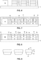
- Figs. 6-8 illustrate assembling the wavelength converting light emitting device.
- individual LEDs 10 which may be the devices illustrated in Fig. 2 or any other suitable device, are attached to a mount 12.
- Individual wavelength converting platelets such as one of the structures illustrated in Figs. 4, 5 , or 9 , are pick-and-place attached to each LED 10.
- a layer of adhesive 50 is cast, dispensed, jetted, or otherwise disposed onto the LED 10 prior to attaching the wavelength converting platelet to the LED. Any suitable adhesive, such as silicone, may be used.
- Any suitable adhesive such as silicone, may be used.
- the wavelength converting platelets are mounted such that the ceramic wavelength converting layer 40 is attached to LED 10 and glass wavelength converting layer 42 is the top layer of the structure.
- glass wavelength converting layer 42 may be attached to LED 10 and ceramic wavelength converting layer 40 may be the top layer of the structure.
- the structure may be heated to cure adhesive 50.
- a bond pad 80 on mount 12 provides electrical connection for multiple LEDs 10.
- a reflective material 52 is pressed into the spaces 56 between neighboring devices.
- Reflective material 52 is shown crosshatched in the figures to distinguish it from other layers.
- Reflective material 52 may be, for example, titanium oxide particles disposed in a transparent material such as silicone.
- Reflective material 52 between individual devices may be necessary to meet specifications for given applications, for example a light and dark contrast specification for automotive headlamps.
- Reflective material may be disposed over individual LEDs 10, as illustrated by reflective material 54, in addition to between neighboring devices.
- reflective material 52 is thinned to remove the material over individual devices, such that light may be emitted through the top surface 55 of wavelength converting layer 42 in each device.
- one or more bond pads 80 on mount 12, which provide electrical connection for multiple LEDs 10 are covered by reflective material 52 in Fig. 7 , which is removed in Fig. 8 .
- Excess reflective material may be removed by any suitable technique.
- excess reflective material is removed by a dry bead blast or a wet bead blast. For example, in a dry bead blast, a stream of air and baking soda particles with an average diameter of 80 ⁇ m may be directed at the surface of the reflective material to remove the excess reflective material.
- plastic particles with an average diameter of 180 ⁇ m in a water slurry are directed at the surface of the reflective material to remove the excess reflective material.
- the top surface 55 of wavelength converting layer 42 is roughened to improve light extraction during removal of excess reflective material illustrated in Fig. 8 .
Landscapes
- Led Device Packages (AREA)
- Optical Filters (AREA)
Claims (15)
- Dispositif électroluminescent comprenant :une structure semi-conductrice comprenant une couche électroluminescente disposée entre une zone de type n et une zone de type p ;une première couche de conversion de longueur d'onde (40) disposée sur un trajet de lumière émise par la couche électroluminescente, la première couche de conversion de longueur d'onde comprenant une céramique de conversion de longueur d'onde ; etune seconde couche de conversion de longueur d'onde (42) fusionnée avec la première couche de conversion de longueur d'onde, la seconde couche de conversion de longueur d'onde comprenant un matériau de conversion de longueur d'onde disposé dans du verre, caractérisé en ce quela première couche de conversion de longueur d'onde est disposée entre la seconde couche de conversion de longueur d'onde et la structure semi-conductrice.
- Dispositif électroluminescent selon la revendication 1, dans lequel la première couche de conversion de longueur d'onde émet une lumière rouge et la seconde couche de conversion de longueur d'onde émet une lumière verte.
- Dispositif électroluminescent selon la revendication 1, dans lequel la première couche de conversion de longueur d'onde et la seconde couche de conversion de longueur d'onde possèdent des parois latérales inclinées.
- Dispositif électroluminescent selon la revendication 1, dans lequel :la première couche de conversion de longueur d'onde et la seconde couche de conversion de longueur d'onde forment un élément de conversion de longueur d'onde ;une première partie de l'élément de conversion de longueur d'onde possède une paroi latérale sensiblement verticale ; etune seconde partie de l'élément de conversion de longueur d'onde possède une paroi verticale inclinée.
- Dispositif électroluminescent selon la revendication 1, comprenant en outre un matériau réfléchissant, dans lequel le matériau réfléchissant est disposé de manière adjacente à chacune d'une paroi latérale de la première couche de conversion de longueur d'onde, d'une paroi latérale de la seconde couche de conversion de longueur d'onde, et d'une paroi latérale de la structure semi-conductrice.
- Procédé comprenant :la formation d'un élément de conversion de longueur d'onde, ladite formation comprenant :la formation d'une première couche de conversion de longueur d'onde, la première couche de conversion de longueur d'onde étant une céramique de conversion de longueur d'onde ;la fusion d'une seconde couche de conversion de longueur d'onde avec la première couche de conversion de longueur d'onde, la fusion d'une seconde couche de conversion de longueur d'onde avec la première couche de conversion de longueur d'onde comprenant :le mélange d'un matériau de conversion de longueur d'onde avec du verre ;le roulage du mélange en une feuille ;la découpe de la feuille afin de l'adapter à la première couche de conversion de longueur d'onde ; etla fusion de la feuille découpée avec la première couche de conversion de longueur d'onde ;la découpe de l'élément de conversion de longueur d'onde en une pluralité de plaquettes ; etaprès ladite découpe, la fixation d'une plaquette sur un dispositif électroluminescent semi-conducteur.
- Procédé selon la revendication 6, dans lequel la formation d'une première couche de conversion de longueur d'onde comprend le frittage d'un phosphore en une tranche.
- Procédé selon la revendication 6, dans lequel la fusion de la feuille découpée comprend le chauffage de la feuille découpée et de la première couche de conversion de longueur d'onde à une température supérieure à une température de refusion du verre.
- Procédé comprenant :la formation d'un élément de conversion de longueur d'onde, ladite formation comprenant :la formation d'une première couche de conversion de longueur d'onde, la première couche de conversion de longueur d'onde étant une céramique de conversion de longueur d'onde ;la fusion d'une seconde couche de conversion de longueur d'onde avec la première couche de conversion de longueur d'onde, la fusion de la seconde couche de conversion de longueur d'onde avec la première couche de conversion de longueur d'onde comprenant :le mélange d'un matériau de conversion de longueur d'onde avec du verre ;le dépôt du mélange sur la première couche de conversion de longueur d'onde ;la répartition du mélange afin de former une couche d'épaisseur sensiblement uniforme ;la découpe de l'élément de conversion de longueur d'onde en une pluralité de plaquettes ; etaprès ladite découpe, la fixation d'une plaquette sur un dispositif électroluminescent semi-conducteur.
- Procédé selon la revendication 6, comprenant en outre l'amincissement de la première couche de conversion de longueur d'onde avant de fusionner la seconde couche de conversion de longueur d'onde avec la première couche de conversion de longueur d'onde.
- Procédé selon la revendication 6, comprenant en outre l'amincissement de la seconde couche de conversion de longueur d'onde après la fusion de la seconde couche de conversion de longueur d'onde avec la première couche de conversion de longueur d'onde.
- Procédé selon la revendication 6 comprenant en outre :la fixation d'une pluralité de dispositifs électroluminescents semi-conducteurs sur un support ;la fixation d'une plaquette sur chaque dispositif électroluminescent semi-conducteur de cette pluralité ;le placement d'un matériau réfléchissant entre les dispositifs électroluminescents semi-conducteurs adjacents de cette pluralité.
- Procédé selon la revendication 12, comprenant en outre l'amincissement du matériau réfléchissant après avoir disposé le matériau réfléchissant entre les dispositifs électroluminescents semi-conducteurs.
- Procédé selon la revendication 6, dans lequel la découpe de l'élément de conversion de longueur d'onde en une pluralité de plaquettes comprend la formation d'une paroi latérale inclinée sur chaque plaquette.
- Procédé selon la revendication 6, dans lequel la découpe de l'élément de conversion de longueur d'onde en une pluralité de plaquettes comprend :la formation, sur une première partie de chaque plaquette, d'une paroi latérale ayant un premier angle par rapport à une surface supérieure de la plaquette ; etla formation, sur une seconde partie de chaque plaquette, d'une paroi latérale ayant un second angle par rapport à une surface supérieure de la plaquette ; etdans lequel le premier angle est différent du second angle.
Applications Claiming Priority (2)
| Application Number | Priority Date | Filing Date | Title |
|---|---|---|---|
| US201361843466P | 2013-07-08 | 2013-07-08 | |
| PCT/IB2014/062813 WO2015004577A1 (fr) | 2013-07-08 | 2014-07-03 | Dispositif électroluminescent à semi-conducteur à conversion de longueur d'onde |
Publications (2)
| Publication Number | Publication Date |
|---|---|
| EP3020076A1 EP3020076A1 (fr) | 2016-05-18 |
| EP3020076B1 true EP3020076B1 (fr) | 2017-09-06 |
Family
ID=51355584
Family Applications (1)
| Application Number | Title | Priority Date | Filing Date |
|---|---|---|---|
| EP14752413.6A Active EP3020076B1 (fr) | 2013-07-08 | 2014-07-03 | Dispositif électroluminescent à semi-conducteur à conversion de longueur d'onde |
Country Status (6)
| Country | Link |
|---|---|
| US (3) | US9761768B2 (fr) |
| EP (1) | EP3020076B1 (fr) |
| JP (2) | JP7068771B2 (fr) |
| KR (1) | KR102180388B1 (fr) |
| CN (2) | CN105493301A (fr) |
| WO (1) | WO2015004577A1 (fr) |
Families Citing this family (29)
| Publication number | Priority date | Publication date | Assignee | Title |
|---|---|---|---|---|
| EP3020076B1 (fr) * | 2013-07-08 | 2017-09-06 | Koninklijke Philips N.V. | Dispositif électroluminescent à semi-conducteur à conversion de longueur d'onde |
| GB201421133D0 (en) * | 2014-11-28 | 2015-01-14 | Cambridge Entpr Ltd | Electroluminescent device |
| TW201631808A (zh) * | 2015-02-25 | 2016-09-01 | 隆達電子股份有限公司 | 發光二極體晶片封裝體 |
| FR3033939B1 (fr) * | 2015-03-20 | 2018-04-27 | Commissariat A L'energie Atomique Et Aux Energies Alternatives | Dispositif optoelectronique a diode electroluminescente |
| DE102015109413A1 (de) * | 2015-06-12 | 2016-12-15 | Osram Opto Semiconductors Gmbh | Verfahren zur Herstellung von optoelektronischen Konversions-Halbleiterchips und Verbund von Konversions-Halbleiterchips |
| JP6217705B2 (ja) * | 2015-07-28 | 2017-10-25 | 日亜化学工業株式会社 | 発光装置及びその製造方法 |
| CN105140377A (zh) | 2015-08-10 | 2015-12-09 | 深圳市华星光电技术有限公司 | 量子点玻璃盒及其制备方法和应用 |
| JP6327220B2 (ja) * | 2015-08-31 | 2018-05-23 | 日亜化学工業株式会社 | 発光装置 |
| FR3049333A1 (fr) * | 2016-03-24 | 2017-09-29 | Valeo Vision | Module de conversion de lumiere, notamment pour vehicule automobile |
| CN107946441A (zh) * | 2016-10-12 | 2018-04-20 | 亿光电子工业股份有限公司 | 发光装置及发光二极管封装结构 |
| US10222681B2 (en) * | 2016-11-07 | 2019-03-05 | Limileds LLC | Segmented light or optical power emitting device with fully converting wavelength converting material and methods of operation |
| KR102689844B1 (ko) * | 2017-01-23 | 2024-07-29 | 삼성디스플레이 주식회사 | 파장 변환 부재 및 이를 포함하는 백라이트 유닛 |
| KR102542426B1 (ko) | 2017-12-20 | 2023-06-12 | 삼성전자주식회사 | 파장변환 필름과, 이를 구비한 반도체 발광장치 |
| US20190198720A1 (en) * | 2017-12-22 | 2019-06-27 | Lumileds Llc | Particle systems and patterning for monolithic led arrays |
| CN109461805B (zh) * | 2018-03-07 | 2021-08-10 | 普瑞光电股份有限公司 | 具有位于包含荧光体的玻璃转换板上的玻璃透镜的汽车led光源 |
| US10756242B2 (en) | 2018-07-30 | 2020-08-25 | Lumileds Llc | Light-emitting device with light scatter tuning to control color shift |
| US10797207B2 (en) | 2018-07-30 | 2020-10-06 | Lumileds Llc | Light emitting device with porous structure to enhance color point shift as a function of drive current |
| CN110875344A (zh) * | 2018-08-31 | 2020-03-10 | 昆山工研院新型平板显示技术中心有限公司 | 一种led显示器件的制备方法及led显示器件 |
| JP7054005B2 (ja) * | 2018-09-28 | 2022-04-13 | 日亜化学工業株式会社 | 発光装置 |
| WO2020083717A1 (fr) * | 2018-10-22 | 2020-04-30 | Lumileds Holding B.V. | Procédé de fabrication de dispositif de conversion de lumière |
| US10910433B2 (en) * | 2018-12-31 | 2021-02-02 | Lumileds Llc | Pixelated LED array with optical elements |
| US11749786B2 (en) | 2019-10-15 | 2023-09-05 | Lumileds Llc | Multicolor phosphor-converted LED array |
| US11063191B2 (en) | 2019-10-15 | 2021-07-13 | Lumileds Llc | Forming a multicolor phosphor-converted LED array |
| EP4046194B1 (fr) * | 2019-10-15 | 2023-08-23 | Lumileds LLC | Formation d'un réseau de del multicolore converti au phosphore |
| US20220285594A1 (en) * | 2019-12-12 | 2022-09-08 | Lumileds Llc | Light emitting diodes with reflective sidewalls comprising porous particles |
| CN113451483A (zh) * | 2020-05-28 | 2021-09-28 | 重庆康佳光电技术研究院有限公司 | 一种颜色转换装置及其制备方法、显示背板 |
| CN113284994B (zh) * | 2021-03-30 | 2023-03-14 | 华灿光电(浙江)有限公司 | 深紫外发光二极管的外延片及其制备方法 |
| KR102625710B1 (ko) * | 2021-09-24 | 2024-01-16 | 주식회사 루츠 | 형광체의 제조방법 |
| CN117917782A (zh) * | 2022-10-20 | 2024-04-23 | 福建中科芯源光电科技有限公司 | 新型封装rgb三色led器件及其制备方法与应用 |
Family Cites Families (82)
| Publication number | Priority date | Publication date | Assignee | Title |
|---|---|---|---|---|
| JP4108790B2 (ja) * | 1997-07-23 | 2008-06-25 | 浜松ホトニクス株式会社 | ガラス部材の接合方法 |
| US5951732A (en) * | 1997-08-27 | 1999-09-14 | Duro; Mark | Method of glass forming |
| JP4280050B2 (ja) * | 2002-10-07 | 2009-06-17 | シチズン電子株式会社 | 白色発光装置 |
| JP2004363380A (ja) * | 2003-06-05 | 2004-12-24 | Sanyo Electric Co Ltd | 光半導体装置およびその製造方法 |
| JP3881653B2 (ja) | 2003-12-25 | 2007-02-14 | 京セラ株式会社 | 発光装置 |
| DE202004006611U1 (de) | 2004-04-23 | 2005-08-25 | Tecpharma Licensing Ag | Injektionsgerät zur Verabreichung eines injizierbaren Produkts mit gesicherter Dosiereinrichtung |
| US7361938B2 (en) * | 2004-06-03 | 2008-04-22 | Philips Lumileds Lighting Company Llc | Luminescent ceramic for a light emitting device |
| US7553683B2 (en) * | 2004-06-09 | 2009-06-30 | Philips Lumiled Lighting Co., Llc | Method of forming pre-fabricated wavelength converting elements for semiconductor light emitting devices |
| WO2006024440A1 (fr) * | 2004-08-28 | 2006-03-09 | Heraeus Quarzglas Gmbh & Co. Kg | Agent d'assemblage pour assembler des elements constitutifs, procede d'assemblage d'elements constitutifs a base d'un materiau contenant de l'acide silicique a haute densite, a l'aide de l'agent d'assemblage et element composite obtenu selon ledit procede |
| US7462502B2 (en) * | 2004-11-12 | 2008-12-09 | Philips Lumileds Lighting Company, Llc | Color control by alteration of wavelength converting element |
| US7419839B2 (en) * | 2004-11-12 | 2008-09-02 | Philips Lumileds Lighting Company, Llc | Bonding an optical element to a light emitting device |
| JP2007048864A (ja) * | 2005-08-09 | 2007-02-22 | Nippon Electric Glass Co Ltd | 蛍光体複合材料 |
| WO2007080555A1 (fr) | 2006-01-16 | 2007-07-19 | Koninklijke Philips Electronics N.V. | Dispositif émetteur de lumière convertie par une substance fluorescente |
| US8441179B2 (en) * | 2006-01-20 | 2013-05-14 | Cree, Inc. | Lighting devices having remote lumiphors that are excited by lumiphor-converted semiconductor excitation sources |
| US7682850B2 (en) * | 2006-03-17 | 2010-03-23 | Philips Lumileds Lighting Company, Llc | White LED for backlight with phosphor plates |
| US8481977B2 (en) * | 2006-03-24 | 2013-07-09 | Goldeneye, Inc. | LED light source with thermally conductive luminescent matrix |
| JP2007324475A (ja) * | 2006-06-02 | 2007-12-13 | Sharp Corp | 波長変換部材および発光装置 |
| JP2009540595A (ja) * | 2006-06-14 | 2009-11-19 | コーニンクレッカ フィリップス エレクトロニクス エヌ ヴィ | 照明デバイス |
| US7521862B2 (en) * | 2006-11-20 | 2009-04-21 | Philips Lumileds Lighting Co., Llc | Light emitting device including luminescent ceramic and light-scattering material |
| EP2097935B1 (fr) * | 2006-12-21 | 2016-10-05 | Koninklijke Philips N.V. | Dispositif d'émission de lumière avec un convertisseur de longueur d'onde profilé |
| US7902564B2 (en) * | 2006-12-22 | 2011-03-08 | Koninklijke Philips Electronics N.V. | Multi-grain luminescent ceramics for light emitting devices |
| JP2008169348A (ja) * | 2007-01-15 | 2008-07-24 | Nippon Electric Glass Co Ltd | 蛍光体複合材料 |
| US8232564B2 (en) * | 2007-01-22 | 2012-07-31 | Cree, Inc. | Wafer level phosphor coating technique for warm light emitting diodes |
| US20090039375A1 (en) * | 2007-08-07 | 2009-02-12 | Cree, Inc. | Semiconductor light emitting devices with separated wavelength conversion materials and methods of forming the same |
| JP2009126725A (ja) * | 2007-11-20 | 2009-06-11 | Canon Inc | ガラス部材の製造方法及び加熱延伸装置 |
| GB0801509D0 (en) * | 2008-01-28 | 2008-03-05 | Photonstar Led Ltd | Light emitting system with optically transparent thermally conductive element |
| KR101592836B1 (ko) * | 2008-02-07 | 2016-02-05 | 미쓰비시 가가꾸 가부시키가이샤 | 반도체 발광 장치, 백라이트, 컬러 화상 표시 장치, 및 그들에 사용하는 형광체 |
| WO2009098654A1 (fr) * | 2008-02-08 | 2009-08-13 | Koninklijke Philips Electronics N.V. | Élément optique et procédé de fabrication de celui-ci |
| US8169136B2 (en) * | 2008-02-21 | 2012-05-01 | Nitto Denko Corporation | Light emitting device with translucent ceramic plate |
| EP2272102B1 (fr) | 2008-03-26 | 2016-06-22 | Panasonic Intellectual Property Management Co., Ltd. | Dispositif émetteur de lumière à semiconducteur |
| US8410681B2 (en) * | 2008-06-30 | 2013-04-02 | Bridgelux, Inc. | Light emitting device having a refractory phosphor layer |
| US10147843B2 (en) * | 2008-07-24 | 2018-12-04 | Lumileds Llc | Semiconductor light emitting device including a window layer and a light-directing structure |
| US7888691B2 (en) * | 2008-08-29 | 2011-02-15 | Koninklijke Philips Electronics N.V. | Light source including a wavelength-converted semiconductor light emitting device and a filter |
| KR101639793B1 (ko) | 2008-09-25 | 2016-07-15 | 코닌클리케 필립스 엔.브이. | 코팅된 발광 장치 및 그 코팅 방법 |
| TWI608760B (zh) * | 2008-11-13 | 2017-12-11 | 行家光電有限公司 | 形成螢光粉轉換發光元件之方法 |
| JP5606922B2 (ja) * | 2008-11-28 | 2014-10-15 | 株式会社小糸製作所 | 発光モジュールおよび灯具ユニット |
| JP5482378B2 (ja) * | 2009-04-20 | 2014-05-07 | 日亜化学工業株式会社 | 発光装置 |
| US20120098017A1 (en) * | 2009-05-15 | 2012-04-26 | Koito Manufacturing Co., Ltd. | Light emitting module, method of producing light-emitting module, and lighting fixture unit |
| JP5410167B2 (ja) | 2009-06-12 | 2014-02-05 | 株式会社小糸製作所 | 発光モジュールおよび車両用前照灯 |
| JP5139519B2 (ja) * | 2009-09-01 | 2013-02-06 | 株式会社東芝 | 半導体発光素子及び半導体発光装置 |
| US8933644B2 (en) * | 2009-09-18 | 2015-01-13 | Soraa, Inc. | LED lamps with improved quality of light |
| JP5638348B2 (ja) * | 2009-11-04 | 2014-12-10 | 宇部マテリアルズ株式会社 | 青色発光蛍光体及び発光装置 |
| US8230720B2 (en) * | 2009-11-19 | 2012-07-31 | Honeywell International Inc. | Functionalized monolayers for carbon dioxide detection by a resonant nanosensor |
| KR20120104377A (ko) | 2009-12-17 | 2012-09-20 | 코닌클리즈케 필립스 일렉트로닉스 엔.브이. | 발광 물질을 갖는 발광 다이오드 소자 |
| DE102010005169A1 (de) * | 2009-12-21 | 2011-06-22 | OSRAM Opto Semiconductors GmbH, 93055 | Strahlungsemittierendes Halbleiterbauelement |
| DE102010009456A1 (de) * | 2010-02-26 | 2011-09-01 | Osram Opto Semiconductors Gmbh | Strahlungsemittierendes Bauelement mit einem Halbleiterchip und einem Konversionselement und Verfahren zu dessen Herstellung |
| JP5749327B2 (ja) * | 2010-03-19 | 2015-07-15 | 日東電工株式会社 | 発光装置用ガーネット系蛍光体セラミックシート |
| US8324798B2 (en) * | 2010-03-19 | 2012-12-04 | Nitto Denko Corporation | Light emitting device using orange-red phosphor with co-dopants |
| DE102010028407B4 (de) * | 2010-04-30 | 2021-01-14 | OSRAM Opto Semiconductors Gesellschaft mit beschränkter Haftung | Optoelektronisches Bauelement und Verfahren zum Herstellen eines optoelektronischen Bauelements |
| JP5249283B2 (ja) * | 2010-05-10 | 2013-07-31 | デクセリアルズ株式会社 | 緑色発光蛍光体粒子及びその製造方法、並びに、色変換シート、発光装置及び画像表示装置組立体 |
| JP2011238778A (ja) * | 2010-05-11 | 2011-11-24 | Konica Minolta Opto Inc | 波長変換素子の製造方法、波長変換素子および発光装置 |
| JP5437177B2 (ja) * | 2010-06-25 | 2014-03-12 | パナソニック株式会社 | 発光装置 |
| JP5854367B2 (ja) * | 2011-06-21 | 2016-02-09 | 日本電気硝子株式会社 | 蛍光体複合部材の製造方法 |
| JP2012036367A (ja) * | 2010-07-14 | 2012-02-23 | Nippon Electric Glass Co Ltd | 蛍光体複合部材 |
| CN102782082A (zh) * | 2010-07-14 | 2012-11-14 | 日本电气硝子株式会社 | 荧光体复合部件、led器件和荧光体复合部件的制造方法 |
| US8941135B2 (en) * | 2010-07-15 | 2015-01-27 | Nitto Denko Corporation | Light emissive ceramic laminate and method of making same |
| CN101931040A (zh) * | 2010-07-20 | 2010-12-29 | 嘉兴嘉尼光电科技有限公司 | Led面光源封装 |
| JP5678509B2 (ja) * | 2010-08-02 | 2015-03-04 | 日本電気硝子株式会社 | 波長変換部材の製造方法、波長変換部材及び光源 |
| JP5421205B2 (ja) * | 2010-08-20 | 2014-02-19 | 株式会社東芝 | 発光装置 |
| JP2012052061A (ja) * | 2010-09-03 | 2012-03-15 | Nippon Electric Glass Co Ltd | 蛍光体複合部材 |
| US8334646B2 (en) * | 2010-09-27 | 2012-12-18 | Osram Sylvania Inc. | LED wavelength-coverting plate with microlenses in multiple layers |
| JP2013539229A (ja) * | 2010-09-29 | 2013-10-17 | コーニンクレッカ フィリップス エヌ ヴェ | 波長変換型発光デバイス |
| DE102010042217A1 (de) | 2010-10-08 | 2012-04-12 | Osram Ag | Optoelektronisches Halbleiterbauelement und Verfahren zu seiner Herstellung |
| US8846172B2 (en) * | 2010-10-18 | 2014-09-30 | Nitto Denko Corporation | Light emissive ceramic laminate and method of making same |
| CN102456807A (zh) | 2010-10-26 | 2012-05-16 | 比亚迪股份有限公司 | 一种led组件及其制备方法 |
| EP2450625B1 (fr) * | 2010-11-08 | 2016-08-17 | LG Innotek Co., Ltd. | Dispositif d'éclairage comportant une plaque photoluminescente |
| JP5671982B2 (ja) * | 2010-11-30 | 2015-02-18 | 三菱化学株式会社 | 半導体発光素子および半導体発光素子の製造方法 |
| JPWO2012132232A1 (ja) * | 2011-03-31 | 2014-07-24 | パナソニック株式会社 | 半導体発光装置 |
| US8884330B2 (en) * | 2011-04-13 | 2014-11-11 | Osram Sylvania Inc. | LED wavelength-converting structure including a thin film structure |
| US8704262B2 (en) * | 2011-08-11 | 2014-04-22 | Goldeneye, Inc. | Solid state light sources with common luminescent and heat dissipating surfaces |
| DE102011114641B4 (de) * | 2011-09-30 | 2021-08-12 | OSRAM Opto Semiconductors Gesellschaft mit beschränkter Haftung | Optoelektronisches Halbleiterbauelement und Verfahren zur Herstellung eines optoelektronischen Halbleiterbauelements |
| JP5928476B2 (ja) * | 2011-10-18 | 2016-06-01 | 株式会社村田製作所 | 発光素子、その製造方法、及び発光デバイス |
| RU2502917C2 (ru) * | 2011-12-30 | 2013-12-27 | Закрытое Акционерное Общество "Научно-Производственная Коммерческая Фирма "Элтан Лтд" | Светодиодный источник белого света с комбинированным удаленным фотолюминесцентным конвертером |
| JP5946036B2 (ja) * | 2012-05-01 | 2016-07-05 | 国立研究開発法人物質・材料研究機構 | 発光装置 |
| CN102723424B (zh) * | 2012-05-25 | 2015-01-21 | 苏州晶品光电科技有限公司 | 一种led用荧光薄片的制备方法 |
| JP5997766B2 (ja) * | 2012-05-31 | 2016-09-28 | パナソニックIpマネジメント株式会社 | Ledモジュール |
| DE102012111123A1 (de) * | 2012-09-26 | 2014-03-27 | Osram Opto Semiconductors Gmbh | Licht emittierendes Halbleiterbauelement |
| US8754435B1 (en) * | 2013-02-19 | 2014-06-17 | Cooledge Lighting Inc. | Engineered-phosphor LED package and related methods |
| EP2968296B1 (fr) * | 2013-03-12 | 2020-09-02 | The Regents of the University of California | Modulateurs de gamma-secrétase |
| CN111628062A (zh) * | 2013-04-11 | 2020-09-04 | 亮锐控股有限公司 | 顶发射式半导体发光器件 |
| EP3020076B1 (fr) * | 2013-07-08 | 2017-09-06 | Koninklijke Philips N.V. | Dispositif électroluminescent à semi-conducteur à conversion de longueur d'onde |
| DE102013111120A1 (de) | 2013-10-08 | 2015-04-09 | Osram Opto Semiconductors Gmbh | Halbleiterchip und Verfahren zum Vereinzeln eines Verbundes in Halbleiterchips |
-
2014
- 2014-07-03 EP EP14752413.6A patent/EP3020076B1/fr active Active
- 2014-07-03 CN CN201480049378.9A patent/CN105493301A/zh active Pending
- 2014-07-03 CN CN202010186790.2A patent/CN111509112B/zh active Active
- 2014-07-03 WO PCT/IB2014/062813 patent/WO2015004577A1/fr not_active Ceased
- 2014-07-03 US US14/903,727 patent/US9761768B2/en active Active
- 2014-07-03 KR KR1020167003406A patent/KR102180388B1/ko active Active
- 2014-07-03 JP JP2016524924A patent/JP7068771B2/ja active Active
-
2017
- 2017-08-17 US US15/679,897 patent/US10270013B2/en active Active
-
2019
- 2019-04-22 US US16/391,064 patent/US10790417B2/en active Active
-
2020
- 2020-01-06 JP JP2020000327A patent/JP7316947B2/ja active Active
Non-Patent Citations (1)
| Title |
|---|
| None * |
Also Published As
| Publication number | Publication date |
|---|---|
| JP2020074419A (ja) | 2020-05-14 |
| CN111509112A (zh) | 2020-08-07 |
| US20190252580A1 (en) | 2019-08-15 |
| JP7316947B2 (ja) | 2023-07-28 |
| EP3020076A1 (fr) | 2016-05-18 |
| CN105493301A (zh) | 2016-04-13 |
| US10790417B2 (en) | 2020-09-29 |
| JP2016524344A (ja) | 2016-08-12 |
| WO2015004577A1 (fr) | 2015-01-15 |
| CN111509112B (zh) | 2024-04-02 |
| JP7068771B2 (ja) | 2022-05-17 |
| KR102180388B1 (ko) | 2020-11-19 |
| US20160163931A1 (en) | 2016-06-09 |
| KR20160032147A (ko) | 2016-03-23 |
| US9761768B2 (en) | 2017-09-12 |
| US10270013B2 (en) | 2019-04-23 |
| US20180033923A1 (en) | 2018-02-01 |
Similar Documents
| Publication | Publication Date | Title |
|---|---|---|
| US10790417B2 (en) | Wavelength converted semiconductor light emitting device | |
| JP5918221B2 (ja) | Ledチップの製造方法 | |
| EP2997610B1 (fr) | Dispositif électroluminescent ayant un élément optique et un réflecteur | |
| EP2917938B1 (fr) | Dispositif électroluminescent à longueur d'onde convertie | |
| US9935244B2 (en) | Light emitting device including a filter and a protective layer | |
| US20180331261A1 (en) | Wavelength converted light emitting device with small source size | |
| EP3111487B1 (fr) | Procédé de formation d'un dispositif électroluminescent à longueur d'onde convertie | |
| KR102227866B1 (ko) | 두꺼운 금속 층들을 갖는 반도체 발광 디바이스 | |
| KR20120128671A (ko) | 발광 다이오드를 위한 파장 변환 층의 형성 방법 |
Legal Events
| Date | Code | Title | Description |
|---|---|---|---|
| PUAI | Public reference made under article 153(3) epc to a published international application that has entered the european phase |
Free format text: ORIGINAL CODE: 0009012 |
|
| 17P | Request for examination filed |
Effective date: 20160208 |
|
| AK | Designated contracting states |
Kind code of ref document: A1 Designated state(s): AL AT BE BG CH CY CZ DE DK EE ES FI FR GB GR HR HU IE IS IT LI LT LU LV MC MK MT NL NO PL PT RO RS SE SI SK SM TR |
|
| AX | Request for extension of the european patent |
Extension state: BA ME |
|
| DAX | Request for extension of the european patent (deleted) | ||
| REG | Reference to a national code |
Ref country code: DE Ref legal event code: R079 Ref document number: 602014014253 Country of ref document: DE Free format text: PREVIOUS MAIN CLASS: H01L0033500000 Ipc: H01L0033000000 |
|
| GRAP | Despatch of communication of intention to grant a patent |
Free format text: ORIGINAL CODE: EPIDOSNIGR1 |
|
| STAA | Information on the status of an ep patent application or granted ep patent |
Free format text: STATUS: GRANT OF PATENT IS INTENDED |
|
| RIC1 | Information provided on ipc code assigned before grant |
Ipc: H01L 33/60 20100101ALI20170316BHEP Ipc: H01L 27/15 20060101AFI20170316BHEP Ipc: H01L 33/50 20100101ALI20170316BHEP |
|
| RIC1 | Information provided on ipc code assigned before grant |
Ipc: H01L 33/00 20100101AFI20170328BHEP Ipc: H01L 33/60 20100101ALI20170328BHEP Ipc: H01L 33/50 20100101ALI20170328BHEP Ipc: H01L 25/075 20060101ALI20170328BHEP |
|
| INTG | Intention to grant announced |
Effective date: 20170411 |
|
| GRAS | Grant fee paid |
Free format text: ORIGINAL CODE: EPIDOSNIGR3 |
|
| GRAA | (expected) grant |
Free format text: ORIGINAL CODE: 0009210 |
|
| STAA | Information on the status of an ep patent application or granted ep patent |
Free format text: STATUS: THE PATENT HAS BEEN GRANTED |
|
| AK | Designated contracting states |
Kind code of ref document: B1 Designated state(s): AL AT BE BG CH CY CZ DE DK EE ES FI FR GB GR HR HU IE IS IT LI LT LU LV MC MK MT NL NO PL PT RO RS SE SI SK SM TR |
|
| REG | Reference to a national code |
Ref country code: GB Ref legal event code: FG4D |
|
| REG | Reference to a national code |
Ref country code: CH Ref legal event code: EP Ref country code: AT Ref legal event code: REF Ref document number: 926747 Country of ref document: AT Kind code of ref document: T Effective date: 20170915 |
|
| REG | Reference to a national code |
Ref country code: IE Ref legal event code: FG4D |
|
| REG | Reference to a national code |
Ref country code: DE Ref legal event code: R096 Ref document number: 602014014253 Country of ref document: DE |
|
| REG | Reference to a national code |
Ref country code: NL Ref legal event code: MP Effective date: 20170906 |
|
| REG | Reference to a national code |
Ref country code: LT Ref legal event code: MG4D |
|
| PG25 | Lapsed in a contracting state [announced via postgrant information from national office to epo] |
Ref country code: LT Free format text: LAPSE BECAUSE OF FAILURE TO SUBMIT A TRANSLATION OF THE DESCRIPTION OR TO PAY THE FEE WITHIN THE PRESCRIBED TIME-LIMIT Effective date: 20170906 Ref country code: FI Free format text: LAPSE BECAUSE OF FAILURE TO SUBMIT A TRANSLATION OF THE DESCRIPTION OR TO PAY THE FEE WITHIN THE PRESCRIBED TIME-LIMIT Effective date: 20170906 Ref country code: NO Free format text: LAPSE BECAUSE OF FAILURE TO SUBMIT A TRANSLATION OF THE DESCRIPTION OR TO PAY THE FEE WITHIN THE PRESCRIBED TIME-LIMIT Effective date: 20171206 Ref country code: HR Free format text: LAPSE BECAUSE OF FAILURE TO SUBMIT A TRANSLATION OF THE DESCRIPTION OR TO PAY THE FEE WITHIN THE PRESCRIBED TIME-LIMIT Effective date: 20170906 Ref country code: SE Free format text: LAPSE BECAUSE OF FAILURE TO SUBMIT A TRANSLATION OF THE DESCRIPTION OR TO PAY THE FEE WITHIN THE PRESCRIBED TIME-LIMIT Effective date: 20170906 |
|
| REG | Reference to a national code |
Ref country code: AT Ref legal event code: MK05 Ref document number: 926747 Country of ref document: AT Kind code of ref document: T Effective date: 20170906 |
|
| PG25 | Lapsed in a contracting state [announced via postgrant information from national office to epo] |
Ref country code: BG Free format text: LAPSE BECAUSE OF FAILURE TO SUBMIT A TRANSLATION OF THE DESCRIPTION OR TO PAY THE FEE WITHIN THE PRESCRIBED TIME-LIMIT Effective date: 20171206 Ref country code: GR Free format text: LAPSE BECAUSE OF FAILURE TO SUBMIT A TRANSLATION OF THE DESCRIPTION OR TO PAY THE FEE WITHIN THE PRESCRIBED TIME-LIMIT Effective date: 20171207 Ref country code: ES Free format text: LAPSE BECAUSE OF FAILURE TO SUBMIT A TRANSLATION OF THE DESCRIPTION OR TO PAY THE FEE WITHIN THE PRESCRIBED TIME-LIMIT Effective date: 20170906 Ref country code: RS Free format text: LAPSE BECAUSE OF FAILURE TO SUBMIT A TRANSLATION OF THE DESCRIPTION OR TO PAY THE FEE WITHIN THE PRESCRIBED TIME-LIMIT Effective date: 20170906 Ref country code: LV Free format text: LAPSE BECAUSE OF FAILURE TO SUBMIT A TRANSLATION OF THE DESCRIPTION OR TO PAY THE FEE WITHIN THE PRESCRIBED TIME-LIMIT Effective date: 20170906 |
|
| PG25 | Lapsed in a contracting state [announced via postgrant information from national office to epo] |
Ref country code: NL Free format text: LAPSE BECAUSE OF FAILURE TO SUBMIT A TRANSLATION OF THE DESCRIPTION OR TO PAY THE FEE WITHIN THE PRESCRIBED TIME-LIMIT Effective date: 20170906 |
|
| PG25 | Lapsed in a contracting state [announced via postgrant information from national office to epo] |
Ref country code: CZ Free format text: LAPSE BECAUSE OF FAILURE TO SUBMIT A TRANSLATION OF THE DESCRIPTION OR TO PAY THE FEE WITHIN THE PRESCRIBED TIME-LIMIT Effective date: 20170906 Ref country code: PL Free format text: LAPSE BECAUSE OF FAILURE TO SUBMIT A TRANSLATION OF THE DESCRIPTION OR TO PAY THE FEE WITHIN THE PRESCRIBED TIME-LIMIT Effective date: 20170906 Ref country code: RO Free format text: LAPSE BECAUSE OF FAILURE TO SUBMIT A TRANSLATION OF THE DESCRIPTION OR TO PAY THE FEE WITHIN THE PRESCRIBED TIME-LIMIT Effective date: 20170906 |
|
| PG25 | Lapsed in a contracting state [announced via postgrant information from national office to epo] |
Ref country code: IS Free format text: LAPSE BECAUSE OF FAILURE TO SUBMIT A TRANSLATION OF THE DESCRIPTION OR TO PAY THE FEE WITHIN THE PRESCRIBED TIME-LIMIT Effective date: 20180106 Ref country code: SM Free format text: LAPSE BECAUSE OF FAILURE TO SUBMIT A TRANSLATION OF THE DESCRIPTION OR TO PAY THE FEE WITHIN THE PRESCRIBED TIME-LIMIT Effective date: 20170906 Ref country code: EE Free format text: LAPSE BECAUSE OF FAILURE TO SUBMIT A TRANSLATION OF THE DESCRIPTION OR TO PAY THE FEE WITHIN THE PRESCRIBED TIME-LIMIT Effective date: 20170906 Ref country code: SK Free format text: LAPSE BECAUSE OF FAILURE TO SUBMIT A TRANSLATION OF THE DESCRIPTION OR TO PAY THE FEE WITHIN THE PRESCRIBED TIME-LIMIT Effective date: 20170906 Ref country code: AT Free format text: LAPSE BECAUSE OF FAILURE TO SUBMIT A TRANSLATION OF THE DESCRIPTION OR TO PAY THE FEE WITHIN THE PRESCRIBED TIME-LIMIT Effective date: 20170906 Ref country code: IT Free format text: LAPSE BECAUSE OF FAILURE TO SUBMIT A TRANSLATION OF THE DESCRIPTION OR TO PAY THE FEE WITHIN THE PRESCRIBED TIME-LIMIT Effective date: 20170906 |
|
| REG | Reference to a national code |
Ref country code: DE Ref legal event code: R097 Ref document number: 602014014253 Country of ref document: DE |
|
| PLBE | No opposition filed within time limit |
Free format text: ORIGINAL CODE: 0009261 |
|
| REG | Reference to a national code |
Ref country code: CH Ref legal event code: PUE Owner name: LUMILEDS HOLDING B.V., NL Free format text: FORMER OWNER: KONINKLIJKE PHILIPS N.V., NL |
|
| STAA | Information on the status of an ep patent application or granted ep patent |
Free format text: STATUS: NO OPPOSITION FILED WITHIN TIME LIMIT |
|
| REG | Reference to a national code |
Ref country code: FR Ref legal event code: PLFP Year of fee payment: 5 |
|
| PG25 | Lapsed in a contracting state [announced via postgrant information from national office to epo] |
Ref country code: DK Free format text: LAPSE BECAUSE OF FAILURE TO SUBMIT A TRANSLATION OF THE DESCRIPTION OR TO PAY THE FEE WITHIN THE PRESCRIBED TIME-LIMIT Effective date: 20170906 |
|
| RAP2 | Party data changed (patent owner data changed or rights of a patent transferred) |
Owner name: LUMILEDS HOLDING B.V. |
|
| 26N | No opposition filed |
Effective date: 20180607 |
|
| PG25 | Lapsed in a contracting state [announced via postgrant information from national office to epo] |
Ref country code: SI Free format text: LAPSE BECAUSE OF FAILURE TO SUBMIT A TRANSLATION OF THE DESCRIPTION OR TO PAY THE FEE WITHIN THE PRESCRIBED TIME-LIMIT Effective date: 20170906 |
|
| REG | Reference to a national code |
Ref country code: DE Ref legal event code: R081 Ref document number: 602014014253 Country of ref document: DE Owner name: LUMILEDS HOLDING B.V., NL Free format text: FORMER OWNER: KONINKLIJKE PHILIPS N.V., EINDHOVEN, NL |
|
| REG | Reference to a national code |
Ref country code: CH Ref legal event code: PL |
|
| PG25 | Lapsed in a contracting state [announced via postgrant information from national office to epo] |
Ref country code: LU Free format text: LAPSE BECAUSE OF NON-PAYMENT OF DUE FEES Effective date: 20180703 Ref country code: MC Free format text: LAPSE BECAUSE OF FAILURE TO SUBMIT A TRANSLATION OF THE DESCRIPTION OR TO PAY THE FEE WITHIN THE PRESCRIBED TIME-LIMIT Effective date: 20170906 |
|
| REG | Reference to a national code |
Ref country code: BE Ref legal event code: MM Effective date: 20180731 |
|
| REG | Reference to a national code |
Ref country code: IE Ref legal event code: MM4A |
|
| PG25 | Lapsed in a contracting state [announced via postgrant information from national office to epo] |
Ref country code: IE Free format text: LAPSE BECAUSE OF NON-PAYMENT OF DUE FEES Effective date: 20180703 Ref country code: LI Free format text: LAPSE BECAUSE OF NON-PAYMENT OF DUE FEES Effective date: 20180731 Ref country code: CH Free format text: LAPSE BECAUSE OF NON-PAYMENT OF DUE FEES Effective date: 20180731 |
|
| PG25 | Lapsed in a contracting state [announced via postgrant information from national office to epo] |
Ref country code: BE Free format text: LAPSE BECAUSE OF NON-PAYMENT OF DUE FEES Effective date: 20180731 |
|
| PG25 | Lapsed in a contracting state [announced via postgrant information from national office to epo] |
Ref country code: MT Free format text: LAPSE BECAUSE OF NON-PAYMENT OF DUE FEES Effective date: 20180703 |
|
| PG25 | Lapsed in a contracting state [announced via postgrant information from national office to epo] |
Ref country code: TR Free format text: LAPSE BECAUSE OF FAILURE TO SUBMIT A TRANSLATION OF THE DESCRIPTION OR TO PAY THE FEE WITHIN THE PRESCRIBED TIME-LIMIT Effective date: 20170906 |
|
| PG25 | Lapsed in a contracting state [announced via postgrant information from national office to epo] |
Ref country code: PT Free format text: LAPSE BECAUSE OF FAILURE TO SUBMIT A TRANSLATION OF THE DESCRIPTION OR TO PAY THE FEE WITHIN THE PRESCRIBED TIME-LIMIT Effective date: 20170906 |
|
| PG25 | Lapsed in a contracting state [announced via postgrant information from national office to epo] |
Ref country code: HU Free format text: LAPSE BECAUSE OF FAILURE TO SUBMIT A TRANSLATION OF THE DESCRIPTION OR TO PAY THE FEE WITHIN THE PRESCRIBED TIME-LIMIT; INVALID AB INITIO Effective date: 20140703 Ref country code: CY Free format text: LAPSE BECAUSE OF FAILURE TO SUBMIT A TRANSLATION OF THE DESCRIPTION OR TO PAY THE FEE WITHIN THE PRESCRIBED TIME-LIMIT Effective date: 20170906 Ref country code: MK Free format text: LAPSE BECAUSE OF NON-PAYMENT OF DUE FEES Effective date: 20170906 |
|
| PG25 | Lapsed in a contracting state [announced via postgrant information from national office to epo] |
Ref country code: AL Free format text: LAPSE BECAUSE OF FAILURE TO SUBMIT A TRANSLATION OF THE DESCRIPTION OR TO PAY THE FEE WITHIN THE PRESCRIBED TIME-LIMIT Effective date: 20170906 |
|
| P01 | Opt-out of the competence of the unified patent court (upc) registered |
Effective date: 20230530 |
|
| REG | Reference to a national code |
Ref country code: DE Ref legal event code: R079 Ref document number: 602014014253 Country of ref document: DE Free format text: PREVIOUS MAIN CLASS: H01L0033000000 Ipc: H10H0020000000 |
|
| PGFP | Annual fee paid to national office [announced via postgrant information from national office to epo] |
Ref country code: DE Payment date: 20250728 Year of fee payment: 12 |
|
| PGFP | Annual fee paid to national office [announced via postgrant information from national office to epo] |
Ref country code: GB Payment date: 20250722 Year of fee payment: 12 |
|
| PGFP | Annual fee paid to national office [announced via postgrant information from national office to epo] |
Ref country code: FR Payment date: 20250725 Year of fee payment: 12 |