EP3021352B1 - Procédé de réduction de la résistance de contact dans un transistor - Google Patents
Procédé de réduction de la résistance de contact dans un transistor Download PDFInfo
- Publication number
- EP3021352B1 EP3021352B1 EP14193119.6A EP14193119A EP3021352B1 EP 3021352 B1 EP3021352 B1 EP 3021352B1 EP 14193119 A EP14193119 A EP 14193119A EP 3021352 B1 EP3021352 B1 EP 3021352B1
- Authority
- EP
- European Patent Office
- Prior art keywords
- iii
- substrate
- drain
- precursor
- inas
- Prior art date
- Legal status (The legal status is an assumption and is not a legal conclusion. Google has not performed a legal analysis and makes no representation as to the accuracy of the status listed.)
- Active
Links
Images


Classifications
-
- H—ELECTRICITY
- H10—SEMICONDUCTOR DEVICES; ELECTRIC SOLID-STATE DEVICES NOT OTHERWISE PROVIDED FOR
- H10D—INORGANIC ELECTRIC SEMICONDUCTOR DEVICES
- H10D30/00—Field-effect transistors [FET]
- H10D30/01—Manufacture or treatment
- H10D30/021—Manufacture or treatment of FETs having insulated gates [IGFET]
- H10D30/024—Manufacture or treatment of FETs having insulated gates [IGFET] of fin field-effect transistors [FinFET]
-
- H—ELECTRICITY
- H10—SEMICONDUCTOR DEVICES; ELECTRIC SOLID-STATE DEVICES NOT OTHERWISE PROVIDED FOR
- H10D—INORGANIC ELECTRIC SEMICONDUCTOR DEVICES
- H10D30/00—Field-effect transistors [FET]
- H10D30/60—Insulated-gate field-effect transistors [IGFET]
- H10D30/62—Fin field-effect transistors [FinFET]
- H10D30/6211—Fin field-effect transistors [FinFET] having fin-shaped semiconductor bodies integral with the bulk semiconductor substrates
-
- H—ELECTRICITY
- H10—SEMICONDUCTOR DEVICES; ELECTRIC SOLID-STATE DEVICES NOT OTHERWISE PROVIDED FOR
- H10D—INORGANIC ELECTRIC SEMICONDUCTOR DEVICES
- H10D30/00—Field-effect transistors [FET]
- H10D30/60—Insulated-gate field-effect transistors [IGFET]
- H10D30/791—Arrangements for exerting mechanical stress on the crystal lattice of the channel regions
- H10D30/797—Arrangements for exerting mechanical stress on the crystal lattice of the channel regions being in source or drain regions, e.g. SiGe source or drain
-
- H—ELECTRICITY
- H10—SEMICONDUCTOR DEVICES; ELECTRIC SOLID-STATE DEVICES NOT OTHERWISE PROVIDED FOR
- H10D—INORGANIC ELECTRIC SEMICONDUCTOR DEVICES
- H10D62/00—Semiconductor bodies, or regions thereof, of devices having potential barriers
- H10D62/10—Shapes, relative sizes or dispositions of the regions of the semiconductor bodies; Shapes of the semiconductor bodies
- H10D62/13—Semiconductor regions connected to electrodes carrying current to be rectified, amplified or switched, e.g. source or drain regions
- H10D62/149—Source or drain regions of field-effect devices
- H10D62/151—Source or drain regions of field-effect devices of IGFETs
-
- H—ELECTRICITY
- H10—SEMICONDUCTOR DEVICES; ELECTRIC SOLID-STATE DEVICES NOT OTHERWISE PROVIDED FOR
- H10D—INORGANIC ELECTRIC SEMICONDUCTOR DEVICES
- H10D62/00—Semiconductor bodies, or regions thereof, of devices having potential barriers
- H10D62/80—Semiconductor bodies, or regions thereof, of devices having potential barriers characterised by the materials
- H10D62/82—Heterojunctions
-
- H—ELECTRICITY
- H10—SEMICONDUCTOR DEVICES; ELECTRIC SOLID-STATE DEVICES NOT OTHERWISE PROVIDED FOR
- H10D—INORGANIC ELECTRIC SEMICONDUCTOR DEVICES
- H10D62/00—Semiconductor bodies, or regions thereof, of devices having potential barriers
- H10D62/80—Semiconductor bodies, or regions thereof, of devices having potential barriers characterised by the materials
- H10D62/85—Semiconductor bodies, or regions thereof, of devices having potential barriers characterised by the materials being Group III-V materials, e.g. GaAs
-
- H—ELECTRICITY
- H10—SEMICONDUCTOR DEVICES; ELECTRIC SOLID-STATE DEVICES NOT OTHERWISE PROVIDED FOR
- H10D—INORGANIC ELECTRIC SEMICONDUCTOR DEVICES
- H10D64/00—Electrodes of devices having potential barriers
- H10D64/20—Electrodes characterised by their shapes, relative sizes or dispositions
- H10D64/23—Electrodes carrying the current to be rectified, amplified, oscillated or switched, e.g. sources, drains, anodes or cathodes
- H10D64/251—Source or drain electrodes for field-effect devices
-
- H—ELECTRICITY
- H10—SEMICONDUCTOR DEVICES; ELECTRIC SOLID-STATE DEVICES NOT OTHERWISE PROVIDED FOR
- H10P—GENERIC PROCESSES OR APPARATUS FOR THE MANUFACTURE OR TREATMENT OF DEVICES COVERED BY CLASS H10
- H10P14/00—Formation of materials, e.g. in the shape of layers or pillars
- H10P14/20—Formation of materials, e.g. in the shape of layers or pillars of semiconductor materials
- H10P14/24—Formation of materials, e.g. in the shape of layers or pillars of semiconductor materials using chemical vapour deposition [CVD]
-
- H—ELECTRICITY
- H10—SEMICONDUCTOR DEVICES; ELECTRIC SOLID-STATE DEVICES NOT OTHERWISE PROVIDED FOR
- H10P—GENERIC PROCESSES OR APPARATUS FOR THE MANUFACTURE OR TREATMENT OF DEVICES COVERED BY CLASS H10
- H10P14/00—Formation of materials, e.g. in the shape of layers or pillars
- H10P14/20—Formation of materials, e.g. in the shape of layers or pillars of semiconductor materials
- H10P14/27—Formation of materials, e.g. in the shape of layers or pillars of semiconductor materials using selective deposition, e.g. simultaneous growth of monocrystalline and non-monocrystalline semiconductor materials
- H10P14/271—Formation of materials, e.g. in the shape of layers or pillars of semiconductor materials using selective deposition, e.g. simultaneous growth of monocrystalline and non-monocrystalline semiconductor materials characterised by the preparation of substrate for selective deposition
-
- H—ELECTRICITY
- H10—SEMICONDUCTOR DEVICES; ELECTRIC SOLID-STATE DEVICES NOT OTHERWISE PROVIDED FOR
- H10P—GENERIC PROCESSES OR APPARATUS FOR THE MANUFACTURE OR TREATMENT OF DEVICES COVERED BY CLASS H10
- H10P14/00—Formation of materials, e.g. in the shape of layers or pillars
- H10P14/20—Formation of materials, e.g. in the shape of layers or pillars of semiconductor materials
- H10P14/29—Formation of materials, e.g. in the shape of layers or pillars of semiconductor materials characterised by the substrates
- H10P14/2901—Materials
- H10P14/2902—Materials being Group IVA materials
- H10P14/2905—Silicon, silicon germanium or germanium
-
- H—ELECTRICITY
- H10—SEMICONDUCTOR DEVICES; ELECTRIC SOLID-STATE DEVICES NOT OTHERWISE PROVIDED FOR
- H10P—GENERIC PROCESSES OR APPARATUS FOR THE MANUFACTURE OR TREATMENT OF DEVICES COVERED BY CLASS H10
- H10P14/00—Formation of materials, e.g. in the shape of layers or pillars
- H10P14/20—Formation of materials, e.g. in the shape of layers or pillars of semiconductor materials
- H10P14/29—Formation of materials, e.g. in the shape of layers or pillars of semiconductor materials characterised by the substrates
- H10P14/2924—Structures
- H10P14/2925—Surface structures
-
- H—ELECTRICITY
- H10—SEMICONDUCTOR DEVICES; ELECTRIC SOLID-STATE DEVICES NOT OTHERWISE PROVIDED FOR
- H10P—GENERIC PROCESSES OR APPARATUS FOR THE MANUFACTURE OR TREATMENT OF DEVICES COVERED BY CLASS H10
- H10P14/00—Formation of materials, e.g. in the shape of layers or pillars
- H10P14/20—Formation of materials, e.g. in the shape of layers or pillars of semiconductor materials
- H10P14/32—Formation of materials, e.g. in the shape of layers or pillars of semiconductor materials characterised by intermediate layers between substrates and deposited layers
- H10P14/3202—Materials thereof
- H10P14/3214—Materials thereof being Group IIIA-VA semiconductors
-
- H—ELECTRICITY
- H10—SEMICONDUCTOR DEVICES; ELECTRIC SOLID-STATE DEVICES NOT OTHERWISE PROVIDED FOR
- H10P—GENERIC PROCESSES OR APPARATUS FOR THE MANUFACTURE OR TREATMENT OF DEVICES COVERED BY CLASS H10
- H10P14/00—Formation of materials, e.g. in the shape of layers or pillars
- H10P14/20—Formation of materials, e.g. in the shape of layers or pillars of semiconductor materials
- H10P14/34—Deposited materials, e.g. layers
- H10P14/3402—Deposited materials, e.g. layers characterised by the chemical composition
- H10P14/3414—Deposited materials, e.g. layers characterised by the chemical composition being group IIIA-VIA materials
- H10P14/3421—Arsenides
-
- H—ELECTRICITY
- H10—SEMICONDUCTOR DEVICES; ELECTRIC SOLID-STATE DEVICES NOT OTHERWISE PROVIDED FOR
- H10P—GENERIC PROCESSES OR APPARATUS FOR THE MANUFACTURE OR TREATMENT OF DEVICES COVERED BY CLASS H10
- H10P14/00—Formation of materials, e.g. in the shape of layers or pillars
- H10P14/20—Formation of materials, e.g. in the shape of layers or pillars of semiconductor materials
- H10P14/34—Deposited materials, e.g. layers
- H10P14/3402—Deposited materials, e.g. layers characterised by the chemical composition
- H10P14/3414—Deposited materials, e.g. layers characterised by the chemical composition being group IIIA-VIA materials
- H10P14/3422—Antimonides
-
- H—ELECTRICITY
- H10—SEMICONDUCTOR DEVICES; ELECTRIC SOLID-STATE DEVICES NOT OTHERWISE PROVIDED FOR
- H10P—GENERIC PROCESSES OR APPARATUS FOR THE MANUFACTURE OR TREATMENT OF DEVICES COVERED BY CLASS H10
- H10P14/00—Formation of materials, e.g. in the shape of layers or pillars
- H10P14/20—Formation of materials, e.g. in the shape of layers or pillars of semiconductor materials
- H10P14/36—Formation of materials, e.g. in the shape of layers or pillars of semiconductor materials characterised by treatments done before the formation of the materials
-
- H—ELECTRICITY
- H10—SEMICONDUCTOR DEVICES; ELECTRIC SOLID-STATE DEVICES NOT OTHERWISE PROVIDED FOR
- H10P—GENERIC PROCESSES OR APPARATUS FOR THE MANUFACTURE OR TREATMENT OF DEVICES COVERED BY CLASS H10
- H10P14/00—Formation of materials, e.g. in the shape of layers or pillars
- H10P14/20—Formation of materials, e.g. in the shape of layers or pillars of semiconductor materials
- H10P14/36—Formation of materials, e.g. in the shape of layers or pillars of semiconductor materials characterised by treatments done before the formation of the materials
- H10P14/3602—In-situ cleaning
-
- H—ELECTRICITY
- H10—SEMICONDUCTOR DEVICES; ELECTRIC SOLID-STATE DEVICES NOT OTHERWISE PROVIDED FOR
- H10W—GENERIC PACKAGES, INTERCONNECTIONS, CONNECTORS OR OTHER CONSTRUCTIONAL DETAILS OF DEVICES COVERED BY CLASS H10
- H10W10/00—Isolation regions in semiconductor bodies between components of integrated devices
- H10W10/01—Manufacture or treatment
- H10W10/011—Manufacture or treatment of isolation regions comprising dielectric materials
- H10W10/014—Manufacture or treatment of isolation regions comprising dielectric materials using trench refilling with dielectric materials, e.g. shallow trench isolations
-
- H—ELECTRICITY
- H10—SEMICONDUCTOR DEVICES; ELECTRIC SOLID-STATE DEVICES NOT OTHERWISE PROVIDED FOR
- H10W—GENERIC PACKAGES, INTERCONNECTIONS, CONNECTORS OR OTHER CONSTRUCTIONAL DETAILS OF DEVICES COVERED BY CLASS H10
- H10W10/00—Isolation regions in semiconductor bodies between components of integrated devices
- H10W10/10—Isolation regions comprising dielectric materials
- H10W10/17—Isolation regions comprising dielectric materials formed using trench refilling with dielectric materials, e.g. shallow trench isolations
-
- H—ELECTRICITY
- H10—SEMICONDUCTOR DEVICES; ELECTRIC SOLID-STATE DEVICES NOT OTHERWISE PROVIDED FOR
- H10P—GENERIC PROCESSES OR APPARATUS FOR THE MANUFACTURE OR TREATMENT OF DEVICES COVERED BY CLASS H10
- H10P14/00—Formation of materials, e.g. in the shape of layers or pillars
- H10P14/20—Formation of materials, e.g. in the shape of layers or pillars of semiconductor materials
- H10P14/29—Formation of materials, e.g. in the shape of layers or pillars of semiconductor materials characterised by the substrates
- H10P14/2901—Materials
- H10P14/2907—Materials being Group IIIA-VA materials
-
- H—ELECTRICITY
- H10—SEMICONDUCTOR DEVICES; ELECTRIC SOLID-STATE DEVICES NOT OTHERWISE PROVIDED FOR
- H10P—GENERIC PROCESSES OR APPARATUS FOR THE MANUFACTURE OR TREATMENT OF DEVICES COVERED BY CLASS H10
- H10P14/00—Formation of materials, e.g. in the shape of layers or pillars
- H10P14/20—Formation of materials, e.g. in the shape of layers or pillars of semiconductor materials
- H10P14/29—Formation of materials, e.g. in the shape of layers or pillars of semiconductor materials characterised by the substrates
- H10P14/2901—Materials
- H10P14/2907—Materials being Group IIIA-VA materials
- H10P14/2909—Phosphides
-
- H—ELECTRICITY
- H10—SEMICONDUCTOR DEVICES; ELECTRIC SOLID-STATE DEVICES NOT OTHERWISE PROVIDED FOR
- H10P—GENERIC PROCESSES OR APPARATUS FOR THE MANUFACTURE OR TREATMENT OF DEVICES COVERED BY CLASS H10
- H10P14/00—Formation of materials, e.g. in the shape of layers or pillars
- H10P14/20—Formation of materials, e.g. in the shape of layers or pillars of semiconductor materials
- H10P14/29—Formation of materials, e.g. in the shape of layers or pillars of semiconductor materials characterised by the substrates
- H10P14/2901—Materials
- H10P14/2907—Materials being Group IIIA-VA materials
- H10P14/2911—Arsenides
-
- H—ELECTRICITY
- H10—SEMICONDUCTOR DEVICES; ELECTRIC SOLID-STATE DEVICES NOT OTHERWISE PROVIDED FOR
- H10P—GENERIC PROCESSES OR APPARATUS FOR THE MANUFACTURE OR TREATMENT OF DEVICES COVERED BY CLASS H10
- H10P14/00—Formation of materials, e.g. in the shape of layers or pillars
- H10P14/20—Formation of materials, e.g. in the shape of layers or pillars of semiconductor materials
- H10P14/32—Formation of materials, e.g. in the shape of layers or pillars of semiconductor materials characterised by intermediate layers between substrates and deposited layers
- H10P14/3242—Structure
- H10P14/3256—Microstructure
Definitions
- the present invention relates to the field of semiconductor devices and their construction. In particular it relates to a method for reducing contact resistance in transistors.
- the gate length in transistors may be smaller than 20 nm.
- Components currently envisioned for this technology node such as Si FinFET and high mobility channel devices need to fulfil stringent requirements concerning their external resistance.
- the external resistance of these devices will need to be reduced to less than 100 ⁇ m for Ge/III-V and less than 180 ⁇ m for Si.
- a large part of the resistance is coming from the contact resistance (contact plug or local interconnect to the source and drain areas).
- SiGe as source or drain material (with a NiSi or Ni(Si)Ge top layer, or even with direct contacting) one is able to achieve much lower contact resistances for both Si pMOS and Ge pMOS than for nMOS devices.
- SiGe germani-level pinning around 0.6eV leads to good ohmic contacts on Ge pMOS, but leads to Schottky barrier contacts on Ge nMOS.
- EP0329400A2 discloses an InP semiconductor thin film formed by a process in which an amorphous GaAs buffer layer allegedly having a good surface flatness, and then an amorphous InP buffer layer allegedly having a good surface flatness are formed on an Si substrate, and then an InP monocrystalline thin film is grown on the InP buffer layer.
- WO2012/148353A2 discloses a substrate comprising a Si-base and an InAs-layer provided on said Si-base where said InAs-layer has a thickness between 100 and 500 nanometers and root-mean-square roughness of the upper surface of said InAs-layer (4) is below 1 nanometer.
- the InAs-layer is provided on a Si-base annealed at 700°C.
- Sepideh Gorji Ghalamestani et al. discloses an investigation of the growth of thin epitaxial layers of InAs on Si (111) substrates by MOVPE and discloses the growth of GaSb layers on InAs.
- the InAs layer is provided on a Si (111) substrate annealed at 700°C. It further discloses that InAs is an attractive material for optical and high-speed devices due to its high electron mobility and narrow direct band gap.
- US2012/0168877 proposes a device having an electrical contact where the conductive contact material is separated from the source or drain region by a III-V material. Such an arrangement allegedly produces improved current flow in the Si or Ge nMOS. The present inventors have however observed that the resistivity of such an arrangement is disappointingly high. There remains therefore a need in the art for new good MOS arrangements, and especially nMOS arrangements, permitting low contact resistivities.
- the present invention originates from the realization by the inventors that III-V materials do not grow well on either Si or Ge and especially on highly doped Si or Ge, leading to low uniformity and to high defect density in the III-V material. This in turn leads to a disappointingly high contact resistivity for III-V materials grown on Si n Ge 1-n substrates.
- the present invention relates to a method for growing a III-V semiconductor structure on an area of a Si n Ge 1-n substrate, wherein n is from 0 to 1, comprising the steps of:
- n may take the value of 0,1 or an intermediate value.
- a cleaning step may be performed by heating up the substrate 5-10 minutes to a temperature between 550-750 °C for n ⁇ 0.5 and 760-950 for n ⁇ 0.5, at a pressure between 50 and 500 mbar under H 2 atmosphere.
- the Si n Ge 1-n substrate involved in step a may be doped/implanted or undoped.
- the III-V semiconductor structure may be of a n-type or of a p-type.
- the present invention is particularly useful for III-V semiconductor of a n-type.
- the III-V semiconductor is InAs.
- InAs is advantageous because the Fermi level is pinned inside the conduction band of InAs leading to a perfect alignment of both metal and InAs conduction band levels.
- the III-V semiconductor structure may form at least a top layer of a source or a drain in a transistor.
- the III-V semiconductor structure may form at least a top layer of a source or a drain in a transistor.
- the semiconductor structure may be the source or the drain in the transistor or, alternatively, the Si n Ge 1-n substrate may be a lower part of a source or a drain in the transistor and the III-V semiconductor structure may be a top layer on that lower part.
- the transistor may be a FinFET and the Si n Ge 1-n substrate may be a fin of the FinFET.
- the source and/or the drain may be embedded in the Si n Ge 1-n substrate (see Fig. 10 top right) or raised (i.e. not embedded) on the Si n Ge 1-n substrate (see Fig. 10 top left).
- the source or drain When the source or drain is said to be embedded in the substrate, this means that the bottom surface of the source or drain is lower than the top surface of the substrate and that the substrate surrounds closely the bottom surface and a bottom part of the side walls of the source or drain.
- the top surface of the source or drain however is higher than the top surface of the substrate and is not surrounded by the substrate.
- the bottom surface of the source or drain is at the same level or higher than than the top surface of the substrate.
- the temperature in step a is preferably set between 800°C and 900°C if n ⁇ 0.5.
- the group V precursor used in step b is a precursor of As.
- the precursor can be organic or inorganic. It can have for general formula MR 3 wherein M is As and each R is independently selected from the group consisting of H and C 1-4 alkyl chains. Examples of suitable precursors are tertiarybutylarsine (for As), AsH 3 (for As).
- the group III precursor used in step d and/or f may be trimethylindium.
- the carrier gases of steps b, d and f are preferably hydrogen.
- a reductive atmosphere is advantageous.
- exposure to the group III precursor can be discontinued while exposure to the group V precursor can be maintained. In that case, exposure to the group III precursor can be restarted for the performance of step f once the substrate reached the target temperature.
- the step f of exposing the nucleation layer to a group III precursor in a carrier gas and to a group V precursor in a carrier gas can be performed by using the same precursors as used in step b.
- the doped region may be from 1 to 10 nm deep. This is advantageous because it creates less stress in the surface and it minimizes short channel behaviour.
- the doped region may be conformal. This is advantageous as it promotes homogeneous growth of the nucleation layer.
- the doping range of the doped region is from 10 18 to 5 x 10 19 cm- 3 , preferably from 10 18 to 10 19 cm -3 . It has surprisingly been found that a doping level within such a relatively low doping range (a typical doping range of the prior art is 10 20 -10 21 cm -3 ) is sufficient to achieve low contact resistivity (below 10 -8 ⁇ . ⁇ m 2 ) for the III-V semiconductor structure.
- step c and d of the present invention permits a low doping level to suffice for achieving highly crystalline III-V structures.
- An effect of the nucleation layer is to allow uniform growth of the III-V material with a low amount of defects.
- the nucleation layer of step d may be conformal. This is advantageous as it promotes the homogenous growth of the III-V semiconductor structure.
- the III-V semiconductor structure may be a crystal comprising facets.
- the presence of facets is a signature of the very high crystalline quality surprisingly achieved for the III-V semiconductor structures obtained in the embodiments of the present invention.
- steps b, d and f may be performed by metal organic vapor phase epitaxy. This is advantageous because this method is conformal and operates at lower temperature than e.g. vapor phase deposition.
- steps a-f may be performed in a metal organic vapour phase epitaxy reactor. This permits to perform all steps in situ in the same reactor, thereby limiting sample manipulations and therefore contaminations and damages.
- steps b, d and f may be performed at a pressure of from 50 to 500 mbars.
- the disclosure relates to a device comprising:
- the Si n Ge 1-n substrate, the features of the doping (nature, conformality, depth,...), the group V element, the nucleation layer, the III-V material, and the III-V semiconductor structure may be as defined in any embodiment of the first aspect of the present invention.
- the contact resistivity of the III-V semiconductor structure may be below 10 -8 ⁇ . ⁇ m 2 .
- present example may relate to a device obtainable by any embodiment of the method of the first aspect of the present invention.
- transistors These are three-terminal devices having a first main electrode such as a drain, a second main electrode such as a source and a control electrode such as a gate for controlling the flow of electrical charges between the first and second main electrodes.
- Example 1 Manufacture of a Si fin comprising an area on which a InAs source (or drain) structure will be grown.
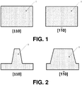
- Figure 1 shows the silicon substrate (1) before formation of the fin.
- the left side of Figure 1 shows a cross-section of the substrate (1) perpendicular to the [110] direction.
- the right side of Figure 1 shows a cross-section of the substrate (1) perpendicular to the [110] direction which is itself perpendicular to the [110] direction.
- the cross-section of the substrate perpendicular to the [110] direction will be referred to as the front cross-sectional view while the cross-section of the substrate perpendicular to the [110] direction will be referred to as the side cross-sectional view.
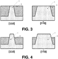
- Figure 2 shows the fin obtained after an etching process operated on the silicon substrate (1). Both cross-sections are cutting in half the area of the substrate where the InAs structure will be grown.
- Figure 3 shows the formation of a shallow trench isolation (STI) by filling trenches present on both sides of the fin with a dielectric material (2) such as SiO 2 .
- a dielectric material (2) such as SiO 2 .
- Figure 4 shows the formation of a recess in the STI so as to uncover a top portion of the fin comprising the area of interest. This can be done by for example wet etch or even a dry etch to recess the STI oxide.
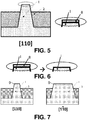
- a native oxide layer (8) was present at the top of the fin. This is represented in Figure 5 .
- Example 2 growing of a InAs source (or drain) structure on the structure of example 1.
- Example 1 The sample of example 1 was placed in a MOVPE (MetalOrganic Vapor Phase Epitaxy) reactor.
- MOVPE MetalOrganic Vapor Phase Epitaxy
- the surface of the fin was thermally cleaned from its native oxide by heating it up to a temperature of 850°C under a H 2 atmosphere at a pressure of less than 100 mbar for a period of from 5 to 10 min. If the substrate is made of Ge instead of Si, the baking should be performed between 550oC and 750oC. For an intermediate composition of the substrate (Si n Ge 1-n ), an intermediate temperature is suitable and can be easily determined by trial and errors.
- the temperature was ramped to higher temperatures (450 - 550°C) with a reactor pressure range between 50mbar and 500mbar in H 2 for the main InAs source (or drain) structure growth.
- the height of the grown structure was about 170 nm above the Si fin level (see Figure 12 where a Scanning Spreading Resistance Microscopy image is shown; on this image, the height of the fins is about 250 nm and the width of the fins is about 45 nm).
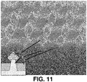
- the grown InAs structure was of high crystalline quality as confirmed by the formation of facets (see Figure 11 where a Transmission Electron Microscopy image is shown).
- Example 3 growing of a InAs layer on a pre-formed source (or drain) structure
- an InAs (or other III-V) layer can be grown on top of a pre-formed Si n Ge 1-n source or drain.
- the same process of example 2 can be repeated except that it starts by cleaning the surface of the pre-formed Si n Ge 1-n source or drain instead of cleaning the fin. It then proceeds by exposing the source or drain surface to an As precursor, exposing the source or drain at a lower temperature to tertiarybutylarsine and trimethylindium until a thickness of InAs of about 5-10 nm is obtained, and growing a layer of InAs at a higher temperature until the desired height is obtained. In this case, InAs is used to reduce the contact resistance of the pre-existing source/drain.
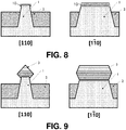
- Figure 10 shows different integration schemes for implementing the source and drain structures of the present invention. Both raised (top left) and embedded (top right) InAs Source/Drain integration schemes can be considered.
- Figure 10 top left and right
- the side cross-sectional view of a fin structure is represented. On top of the fin (1), an InAs source (3) and an InAs drain (3) are shown separated by a gate structure (4) and spacers (11). W connectors (5) and Cu contacts (6) are electrically connected to the source (3) and drain (3).
- the InAs layer can also be used as a thin layer (see example 3 and Figure 10 , bottom) on top of an in-situ doped Si (embedded or raised) source/drain.
- the InAs layer can be used as a thin layer on top of a Ge or SiGe source/drain.
Landscapes
- Insulated Gate Type Field-Effect Transistor (AREA)
Claims (11)
- Procédé de croissance d'une structure à semi-conducteurs III-V (3) sur une zone d'un substrat de SinGe1-n (1), dans lequel n'est compris entre 0 et 1, en formant ainsi au moins une couche supérieure d'une source ou d'un drain dans un transistor situé sur ladite zone, comprenant les étapes consistant à :a. établir la température du substrat de SinGe1-n (1) entre 550°C et 750°C si n < 0,5 et entre 760 et 950°C si n ≥ 0,5,b. à la même température, exposer la zone à un précurseur du groupe V dans un gaz porteur pendant 5 à 30 min, en formant ainsi une région dopée (9) au niveau de ladite zone,c. établir la température du substrat de SinGe1-n (1) entre 325°C et 375°C,d. à la même température, exposer la région dopée à un précurseur du groupe III dans un gaz porteur et à un précurseur du groupe V dans un gaz porteur jusqu'à ce qu'une couche de nucléation (10) de matériau III-V de 5 à 15 nm soit formée sur le région dopée (9),e. établir la température du substrat de SinGe1-n (1) entre 450°C et 550°C,f. à la même température, exposer la couche de nucléation (10) à un précurseur du groupe III dans un gaz porteur et à un précurseur du groupe V dans un gaz porteur, en formant ainsi la structure à semi-conducteurs III-V (3),
dans lequel la structure à semi-conducteurs III-V (3) est InAs,
caractérisé en ce que, à l'étape a, la température est établie entre 850 et 950°C si n = 1,
caractérisé en outre en ce que, à l'étape b, la région dopée a une plage de dopage de 1018 à 5 x 1019 cm-3. - Procédé selon la revendication 1, dans lequel le transistor est un FinFET et dans lequel le substrat de SinGe1-n (1) est une ailette du FinFET.
- Procédé selon la revendication 1 ou la revendication 2, dans lequel la structure à semi-conducteurs III-V (3) est la source ou le drain dans le transistor.
- Procédé selon la revendication 1 ou la revendication 2, dans lequel le substrat de SinGe1-n est une partie inférieure (7) d'une source de SinGe1-n ou d'un drain dans le transistor et dans lequel la structure à semi-conducteurs d'InAs (3) est une couche supérieure sur la partie inférieure (7).
- Procédé selon l'une quelconque des revendications précédentes, dans lequel le précurseur du groupe V utilisé à l'étape b est un précurseur d'As.
- Procédé selon l'une quelconque des revendications précédentes, dans lequel les gaz porteurs des étapes b, d et f sont de l'hydrogène.
- Procédé selon l'une quelconque des revendications précédentes, dans lequel la région dopée (9) a une profondeur de 1 à 10 nm.
- Procédé selon l'une quelconque des revendications précédentes, dans lequel la plage de dopage de la région dopée (9) est de 1018 à 1019 cm-3.
- Procédé selon l'une quelconque des revendications précédentes, dans lequel la structure à semi-conducteurs d'InAs (3) est un cristal comportant des facettes.
- Procédé selon l'une quelconque des revendications précédentes, dans lequel les étapes b, d et f sont réalisées par épitaxie en phase vapeur aux organométalliques.
- Procédé selon l'une quelconque des revendications précédentes, dans lequel les étapes b, d et f sont effectuées à une pression de 50 à 500 mbars.
Priority Applications (2)
| Application Number | Priority Date | Filing Date | Title |
|---|---|---|---|
| EP14193119.6A EP3021352B1 (fr) | 2014-11-13 | 2014-11-13 | Procédé de réduction de la résistance de contact dans un transistor |
| US14/938,169 US9419110B2 (en) | 2014-11-13 | 2015-11-11 | Method for reducing contact resistance in MOS |
Applications Claiming Priority (1)
| Application Number | Priority Date | Filing Date | Title |
|---|---|---|---|
| EP14193119.6A EP3021352B1 (fr) | 2014-11-13 | 2014-11-13 | Procédé de réduction de la résistance de contact dans un transistor |
Publications (2)
| Publication Number | Publication Date |
|---|---|
| EP3021352A1 EP3021352A1 (fr) | 2016-05-18 |
| EP3021352B1 true EP3021352B1 (fr) | 2020-10-07 |
Family
ID=51870942
Family Applications (1)
| Application Number | Title | Priority Date | Filing Date |
|---|---|---|---|
| EP14193119.6A Active EP3021352B1 (fr) | 2014-11-13 | 2014-11-13 | Procédé de réduction de la résistance de contact dans un transistor |
Country Status (2)
| Country | Link |
|---|---|
| US (1) | US9419110B2 (fr) |
| EP (1) | EP3021352B1 (fr) |
Families Citing this family (5)
| Publication number | Priority date | Publication date | Assignee | Title |
|---|---|---|---|---|
| EP3021352B1 (fr) * | 2014-11-13 | 2020-10-07 | IMEC vzw | Procédé de réduction de la résistance de contact dans un transistor |
| KR102310076B1 (ko) | 2015-04-23 | 2021-10-08 | 삼성전자주식회사 | 비대칭 소스/드레인 포함하는 반도체 소자 |
| US10096473B2 (en) * | 2016-04-07 | 2018-10-09 | Aixtron Se | Formation of a layer on a semiconductor substrate |
| US10629708B2 (en) * | 2017-11-14 | 2020-04-21 | Taiwan Semiconductor Manufacturing Co., Ltd. | Semiconductor device structure with barrier layer and method for forming the same |
| US20200373200A1 (en) | 2019-05-24 | 2020-11-26 | Applied Materials, Inc. | Metal based hydrogen barrier |
Family Cites Families (19)
| Publication number | Priority date | Publication date | Assignee | Title |
|---|---|---|---|---|
| JPH01207920A (ja) * | 1988-02-16 | 1989-08-21 | Oki Electric Ind Co Ltd | InP半導体薄膜の製造方法 |
| US6010937A (en) * | 1995-09-05 | 2000-01-04 | Spire Corporation | Reduction of dislocations in a heteroepitaxial semiconductor structure |
| US20070262296A1 (en) * | 2006-05-11 | 2007-11-15 | Matthias Bauer | Photodetectors employing germanium layers |
| JP2010521810A (ja) * | 2007-03-16 | 2010-06-24 | セバスチャン ローデュドス、 | 半導体ヘテロ構造及びその製造 |
| KR100972842B1 (ko) * | 2007-09-11 | 2010-07-28 | 포항공과대학교 산학협력단 | 나노막대를 포함하는 나노디바이스 및 그 제조 방법 |
| KR101030531B1 (ko) * | 2008-12-24 | 2011-04-25 | 엘지디스플레이 주식회사 | 전계방출장치, 전계방출 표시장치 및 그 제조 방법 |
| WO2010118529A1 (fr) * | 2009-04-17 | 2010-10-21 | Arise Technologies Corporation | Structure de base pour dispositifs a semi-conducteur iii-v sur des substrats de groupe iv et son procédé de fabrication |
| US8290014B2 (en) * | 2010-03-11 | 2012-10-16 | Junesand Carl | Active photonic device |
| US8415751B2 (en) | 2010-12-30 | 2013-04-09 | Intel Corporation | Method to reduce contact resistance of N-channel transistors by using a III-V semiconductor interlayer in source and drain |
| US20140048851A1 (en) * | 2011-04-29 | 2014-02-20 | Qunano Ab | Substrate comprising si-base and inas-layer |
| US8872159B2 (en) * | 2011-09-29 | 2014-10-28 | The United States Of America, As Represented By The Secretary Of The Navy | Graphene on semiconductor detector |
| US8896066B2 (en) | 2011-12-20 | 2014-11-25 | Intel Corporation | Tin doped III-V material contacts |
| CN106847811B (zh) * | 2011-12-20 | 2021-04-27 | 英特尔公司 | 减小的接触电阻的自对准接触金属化 |
| KR101635028B1 (ko) | 2011-12-20 | 2016-07-01 | 인텔 코포레이션 | 소스 및 드레인 스트레서들을 이용하는 변형된 채널 영역 트랜지스터들 및 이를 포함하는 시스템들 |
| KR101790153B1 (ko) | 2011-12-27 | 2017-10-26 | 인텔 코포레이션 | 반도체 표면-근처 층의 도핑 농도를 증대시키는 방법 및 그의 제조 방법 |
| EP2775528B1 (fr) * | 2013-03-05 | 2019-07-17 | IMEC vzw | Transistor à effet de champ passivé en forme d'ailette Ge ou III-V |
| US9553174B2 (en) * | 2014-03-28 | 2017-01-24 | Applied Materials, Inc. | Conversion process utilized for manufacturing advanced 3D features for semiconductor device applications |
| US9293523B2 (en) * | 2014-06-24 | 2016-03-22 | Applied Materials, Inc. | Method of forming III-V channel |
| EP3021352B1 (fr) * | 2014-11-13 | 2020-10-07 | IMEC vzw | Procédé de réduction de la résistance de contact dans un transistor |
-
2014
- 2014-11-13 EP EP14193119.6A patent/EP3021352B1/fr active Active
-
2015
- 2015-11-11 US US14/938,169 patent/US9419110B2/en active Active
Non-Patent Citations (1)
| Title |
|---|
| SEPIDEH GORJI GHALAMESTANI ET AL: "High quality InAs and GaSb thin layers grown on Si (111)", JOURNAL OF CRYSTAL GROWTH, ELSEVIER, AMSTERDAM, NL, vol. 332, no. 1, 29 March 2011 (2011-03-29), pages 12 - 16, XP028280485, ISSN: 0022-0248, [retrieved on 20110721], DOI: 10.1016/J.JCRYSGRO.2011.03.062 * |
Also Published As
| Publication number | Publication date |
|---|---|
| US20160141391A1 (en) | 2016-05-19 |
| EP3021352A1 (fr) | 2016-05-18 |
| US9419110B2 (en) | 2016-08-16 |
Similar Documents
| Publication | Publication Date | Title |
|---|---|---|
| US7534675B2 (en) | Techniques for fabricating nanowire field-effect transistors | |
| JP5063594B2 (ja) | 転位欠陥密度の低い格子不整合半導体構造およびこれに関連するデバイス製造方法 | |
| US7795677B2 (en) | Nanowire field-effect transistors | |
| US10971626B2 (en) | Interface charge reduction for SiGe surface | |
| US8609517B2 (en) | MOCVD for growing III-V compound semiconductors on silicon substrates | |
| TWI623042B (zh) | 量子井為基的半導體裝置及其形成方法 | |
| TWI423439B (zh) | 半導體裝置及半導體結構之製造方法 | |
| US9437496B1 (en) | Merged source drain epitaxy | |
| EP3021352B1 (fr) | Procédé de réduction de la résistance de contact dans un transistor | |
| TW200949908A (en) | Semiconductor substrate, method for manufacturing the same and electronic device | |
| CN103094089A (zh) | 鳍式场效应晶体管栅极氧化物 | |
| Waldron et al. | Replacement fin processing for III–V on Si: From FinFets to nanowires | |
| CN107039514A (zh) | Iii‑v族纳米线隧穿fet的方法及结构 | |
| US9614082B2 (en) | Al-poor barrier for InGaAs semiconductor structure | |
| CN1319124C (zh) | 制造绝缘体上半导体沟道结构的方法 | |
| US9087775B2 (en) | Planar semiconductor growth on III-V material | |
| US10784352B2 (en) | Method to achieve a uniform Group IV material layer in an aspect ratio trapping trench | |
| US9735155B2 (en) | Bulk silicon germanium FinFET | |
| Cantoro et al. | Towards the monolithic integration of III-V compound semiconductors on Si: Selective area growth in high aspect ratio structures vs. strain relaxed buffer-mediated epitaxy | |
| CN105226087A (zh) | 具有突变隧穿结的绝缘层上张应变锗tfet及制备方法 | |
| HK1175588B (en) | Quantum-well-based semiconductor devices |
Legal Events
| Date | Code | Title | Description |
|---|---|---|---|
| PUAI | Public reference made under article 153(3) epc to a published international application that has entered the european phase |
Free format text: ORIGINAL CODE: 0009012 |
|
| AK | Designated contracting states |
Kind code of ref document: A1 Designated state(s): AL AT BE BG CH CY CZ DE DK EE ES FI FR GB GR HR HU IE IS IT LI LT LU LV MC MK MT NL NO PL PT RO RS SE SI SK SM TR |
|
| AX | Request for extension of the european patent |
Extension state: BA ME |
|
| STAA | Information on the status of an ep patent application or granted ep patent |
Free format text: STATUS: REQUEST FOR EXAMINATION WAS MADE |
|
| STAA | Information on the status of an ep patent application or granted ep patent |
Free format text: STATUS: EXAMINATION IS IN PROGRESS |
|
| 17P | Request for examination filed |
Effective date: 20161117 |
|
| RBV | Designated contracting states (corrected) |
Designated state(s): AL AT BE BG CH CY CZ DE DK EE ES FI FR GB GR HR HU IE IS IT LI LT LU LV MC MK MT NL NO PL PT RO RS SE SI SK SM TR |
|
| 17Q | First examination report despatched |
Effective date: 20170102 |
|
| REG | Reference to a national code |
Ref country code: DE Ref legal event code: R079 Ref document number: 602014070938 Country of ref document: DE Free format text: PREVIOUS MAIN CLASS: H01L0021020000 Ipc: H01L0021200000 |
|
| GRAP | Despatch of communication of intention to grant a patent |
Free format text: ORIGINAL CODE: EPIDOSNIGR1 |
|
| STAA | Information on the status of an ep patent application or granted ep patent |
Free format text: STATUS: GRANT OF PATENT IS INTENDED |
|
| RIC1 | Information provided on ipc code assigned before grant |
Ipc: H01L 21/20 20060101AFI20200714BHEP Ipc: H01L 21/205 20060101ALI20200714BHEP |
|
| INTG | Intention to grant announced |
Effective date: 20200729 |
|
| GRAS | Grant fee paid |
Free format text: ORIGINAL CODE: EPIDOSNIGR3 |
|
| GRAA | (expected) grant |
Free format text: ORIGINAL CODE: 0009210 |
|
| STAA | Information on the status of an ep patent application or granted ep patent |
Free format text: STATUS: THE PATENT HAS BEEN GRANTED |
|
| AK | Designated contracting states |
Kind code of ref document: B1 Designated state(s): AL AT BE BG CH CY CZ DE DK EE ES FI FR GB GR HR HU IE IS IT LI LT LU LV MC MK MT NL NO PL PT RO RS SE SI SK SM TR |
|
| REG | Reference to a national code |
Ref country code: GB Ref legal event code: FG4D |
|
| REG | Reference to a national code |
Ref country code: AT Ref legal event code: REF Ref document number: 1322046 Country of ref document: AT Kind code of ref document: T Effective date: 20201015 Ref country code: CH Ref legal event code: EP |
|
| REG | Reference to a national code |
Ref country code: IE Ref legal event code: FG4D |
|
| REG | Reference to a national code |
Ref country code: DE Ref legal event code: R096 Ref document number: 602014070938 Country of ref document: DE |
|
| REG | Reference to a national code |
Ref country code: NL Ref legal event code: MP Effective date: 20201007 |
|
| REG | Reference to a national code |
Ref country code: AT Ref legal event code: MK05 Ref document number: 1322046 Country of ref document: AT Kind code of ref document: T Effective date: 20201007 |
|
| PG25 | Lapsed in a contracting state [announced via postgrant information from national office to epo] |
Ref country code: NO Free format text: LAPSE BECAUSE OF FAILURE TO SUBMIT A TRANSLATION OF THE DESCRIPTION OR TO PAY THE FEE WITHIN THE PRESCRIBED TIME-LIMIT Effective date: 20210107 Ref country code: PT Free format text: LAPSE BECAUSE OF FAILURE TO SUBMIT A TRANSLATION OF THE DESCRIPTION OR TO PAY THE FEE WITHIN THE PRESCRIBED TIME-LIMIT Effective date: 20210208 Ref country code: NL Free format text: LAPSE BECAUSE OF FAILURE TO SUBMIT A TRANSLATION OF THE DESCRIPTION OR TO PAY THE FEE WITHIN THE PRESCRIBED TIME-LIMIT Effective date: 20201007 Ref country code: FI Free format text: LAPSE BECAUSE OF FAILURE TO SUBMIT A TRANSLATION OF THE DESCRIPTION OR TO PAY THE FEE WITHIN THE PRESCRIBED TIME-LIMIT Effective date: 20201007 Ref country code: RS Free format text: LAPSE BECAUSE OF FAILURE TO SUBMIT A TRANSLATION OF THE DESCRIPTION OR TO PAY THE FEE WITHIN THE PRESCRIBED TIME-LIMIT Effective date: 20201007 Ref country code: GR Free format text: LAPSE BECAUSE OF FAILURE TO SUBMIT A TRANSLATION OF THE DESCRIPTION OR TO PAY THE FEE WITHIN THE PRESCRIBED TIME-LIMIT Effective date: 20210108 |
|
| REG | Reference to a national code |
Ref country code: LT Ref legal event code: MG4D |
|
| PG25 | Lapsed in a contracting state [announced via postgrant information from national office to epo] |
Ref country code: SE Free format text: LAPSE BECAUSE OF FAILURE TO SUBMIT A TRANSLATION OF THE DESCRIPTION OR TO PAY THE FEE WITHIN THE PRESCRIBED TIME-LIMIT Effective date: 20201007 Ref country code: LV Free format text: LAPSE BECAUSE OF FAILURE TO SUBMIT A TRANSLATION OF THE DESCRIPTION OR TO PAY THE FEE WITHIN THE PRESCRIBED TIME-LIMIT Effective date: 20201007 Ref country code: IS Free format text: LAPSE BECAUSE OF FAILURE TO SUBMIT A TRANSLATION OF THE DESCRIPTION OR TO PAY THE FEE WITHIN THE PRESCRIBED TIME-LIMIT Effective date: 20210207 Ref country code: PL Free format text: LAPSE BECAUSE OF FAILURE TO SUBMIT A TRANSLATION OF THE DESCRIPTION OR TO PAY THE FEE WITHIN THE PRESCRIBED TIME-LIMIT Effective date: 20201007 Ref country code: ES Free format text: LAPSE BECAUSE OF FAILURE TO SUBMIT A TRANSLATION OF THE DESCRIPTION OR TO PAY THE FEE WITHIN THE PRESCRIBED TIME-LIMIT Effective date: 20201007 Ref country code: AT Free format text: LAPSE BECAUSE OF FAILURE TO SUBMIT A TRANSLATION OF THE DESCRIPTION OR TO PAY THE FEE WITHIN THE PRESCRIBED TIME-LIMIT Effective date: 20201007 Ref country code: BG Free format text: LAPSE BECAUSE OF FAILURE TO SUBMIT A TRANSLATION OF THE DESCRIPTION OR TO PAY THE FEE WITHIN THE PRESCRIBED TIME-LIMIT Effective date: 20210107 |
|
| PG25 | Lapsed in a contracting state [announced via postgrant information from national office to epo] |
Ref country code: HR Free format text: LAPSE BECAUSE OF FAILURE TO SUBMIT A TRANSLATION OF THE DESCRIPTION OR TO PAY THE FEE WITHIN THE PRESCRIBED TIME-LIMIT Effective date: 20201007 |
|
| REG | Reference to a national code |
Ref country code: CH Ref legal event code: PL |
|
| REG | Reference to a national code |
Ref country code: DE Ref legal event code: R097 Ref document number: 602014070938 Country of ref document: DE |
|
| PG25 | Lapsed in a contracting state [announced via postgrant information from national office to epo] |
Ref country code: SM Free format text: LAPSE BECAUSE OF FAILURE TO SUBMIT A TRANSLATION OF THE DESCRIPTION OR TO PAY THE FEE WITHIN THE PRESCRIBED TIME-LIMIT Effective date: 20201007 Ref country code: CZ Free format text: LAPSE BECAUSE OF FAILURE TO SUBMIT A TRANSLATION OF THE DESCRIPTION OR TO PAY THE FEE WITHIN THE PRESCRIBED TIME-LIMIT Effective date: 20201007 Ref country code: EE Free format text: LAPSE BECAUSE OF FAILURE TO SUBMIT A TRANSLATION OF THE DESCRIPTION OR TO PAY THE FEE WITHIN THE PRESCRIBED TIME-LIMIT Effective date: 20201007 Ref country code: RO Free format text: LAPSE BECAUSE OF FAILURE TO SUBMIT A TRANSLATION OF THE DESCRIPTION OR TO PAY THE FEE WITHIN THE PRESCRIBED TIME-LIMIT Effective date: 20201007 Ref country code: SK Free format text: LAPSE BECAUSE OF FAILURE TO SUBMIT A TRANSLATION OF THE DESCRIPTION OR TO PAY THE FEE WITHIN THE PRESCRIBED TIME-LIMIT Effective date: 20201007 Ref country code: MC Free format text: LAPSE BECAUSE OF FAILURE TO SUBMIT A TRANSLATION OF THE DESCRIPTION OR TO PAY THE FEE WITHIN THE PRESCRIBED TIME-LIMIT Effective date: 20201007 Ref country code: LU Free format text: LAPSE BECAUSE OF NON-PAYMENT OF DUE FEES Effective date: 20201113 Ref country code: LT Free format text: LAPSE BECAUSE OF FAILURE TO SUBMIT A TRANSLATION OF THE DESCRIPTION OR TO PAY THE FEE WITHIN THE PRESCRIBED TIME-LIMIT Effective date: 20201007 |
|
| REG | Reference to a national code |
Ref country code: BE Ref legal event code: MM Effective date: 20201130 |
|
| PLBE | No opposition filed within time limit |
Free format text: ORIGINAL CODE: 0009261 |
|
| STAA | Information on the status of an ep patent application or granted ep patent |
Free format text: STATUS: NO OPPOSITION FILED WITHIN TIME LIMIT |
|
| PG25 | Lapsed in a contracting state [announced via postgrant information from national office to epo] |
Ref country code: DK Free format text: LAPSE BECAUSE OF FAILURE TO SUBMIT A TRANSLATION OF THE DESCRIPTION OR TO PAY THE FEE WITHIN THE PRESCRIBED TIME-LIMIT Effective date: 20201007 Ref country code: CH Free format text: LAPSE BECAUSE OF NON-PAYMENT OF DUE FEES Effective date: 20201130 Ref country code: LI Free format text: LAPSE BECAUSE OF NON-PAYMENT OF DUE FEES Effective date: 20201130 |
|
| 26N | No opposition filed |
Effective date: 20210708 |
|
| GBPC | Gb: european patent ceased through non-payment of renewal fee |
Effective date: 20210107 |
|
| PG25 | Lapsed in a contracting state [announced via postgrant information from national office to epo] |
Ref country code: FR Free format text: LAPSE BECAUSE OF NON-PAYMENT OF DUE FEES Effective date: 20201207 Ref country code: AL Free format text: LAPSE BECAUSE OF FAILURE TO SUBMIT A TRANSLATION OF THE DESCRIPTION OR TO PAY THE FEE WITHIN THE PRESCRIBED TIME-LIMIT Effective date: 20201007 Ref country code: IT Free format text: LAPSE BECAUSE OF FAILURE TO SUBMIT A TRANSLATION OF THE DESCRIPTION OR TO PAY THE FEE WITHIN THE PRESCRIBED TIME-LIMIT Effective date: 20201007 Ref country code: IE Free format text: LAPSE BECAUSE OF NON-PAYMENT OF DUE FEES Effective date: 20201113 |
|
| PG25 | Lapsed in a contracting state [announced via postgrant information from national office to epo] |
Ref country code: GB Free format text: LAPSE BECAUSE OF NON-PAYMENT OF DUE FEES Effective date: 20210107 Ref country code: SI Free format text: LAPSE BECAUSE OF FAILURE TO SUBMIT A TRANSLATION OF THE DESCRIPTION OR TO PAY THE FEE WITHIN THE PRESCRIBED TIME-LIMIT Effective date: 20201007 |
|
| PG25 | Lapsed in a contracting state [announced via postgrant information from national office to epo] |
Ref country code: IS Free format text: LAPSE BECAUSE OF FAILURE TO SUBMIT A TRANSLATION OF THE DESCRIPTION OR TO PAY THE FEE WITHIN THE PRESCRIBED TIME-LIMIT Effective date: 20210207 Ref country code: TR Free format text: LAPSE BECAUSE OF FAILURE TO SUBMIT A TRANSLATION OF THE DESCRIPTION OR TO PAY THE FEE WITHIN THE PRESCRIBED TIME-LIMIT Effective date: 20201007 Ref country code: MT Free format text: LAPSE BECAUSE OF FAILURE TO SUBMIT A TRANSLATION OF THE DESCRIPTION OR TO PAY THE FEE WITHIN THE PRESCRIBED TIME-LIMIT Effective date: 20201007 Ref country code: CY Free format text: LAPSE BECAUSE OF FAILURE TO SUBMIT A TRANSLATION OF THE DESCRIPTION OR TO PAY THE FEE WITHIN THE PRESCRIBED TIME-LIMIT Effective date: 20201007 |
|
| PG25 | Lapsed in a contracting state [announced via postgrant information from national office to epo] |
Ref country code: MK Free format text: LAPSE BECAUSE OF FAILURE TO SUBMIT A TRANSLATION OF THE DESCRIPTION OR TO PAY THE FEE WITHIN THE PRESCRIBED TIME-LIMIT Effective date: 20201007 |
|
| PG25 | Lapsed in a contracting state [announced via postgrant information from national office to epo] |
Ref country code: BE Free format text: LAPSE BECAUSE OF NON-PAYMENT OF DUE FEES Effective date: 20201130 |
|
| P01 | Opt-out of the competence of the unified patent court (upc) registered |
Effective date: 20230513 |
|
| REG | Reference to a national code |
Ref country code: DE Ref legal event code: R079 Ref document number: 602014070938 Country of ref document: DE Free format text: PREVIOUS MAIN CLASS: H01L0021200000 Ipc: H10P0014200000 |
|
| PGFP | Annual fee paid to national office [announced via postgrant information from national office to epo] |
Ref country code: DE Payment date: 20251022 Year of fee payment: 12 |