EP3023833A1 - Polariseur à filtre intégré coloré et son procédé de fabrication - Google Patents
Polariseur à filtre intégré coloré et son procédé de fabrication Download PDFInfo
- Publication number
- EP3023833A1 EP3023833A1 EP15179831.1A EP15179831A EP3023833A1 EP 3023833 A1 EP3023833 A1 EP 3023833A1 EP 15179831 A EP15179831 A EP 15179831A EP 3023833 A1 EP3023833 A1 EP 3023833A1
- Authority
- EP
- European Patent Office
- Prior art keywords
- holes
- color filter
- polarizer
- region
- resin layer
- Prior art date
- Legal status (The legal status is an assumption and is not a legal conclusion. Google has not performed a legal analysis and makes no representation as to the accuracy of the status listed.)
- Granted
Links
Images







Classifications
-
- G—PHYSICS
- G02—OPTICS
- G02B—OPTICAL ELEMENTS, SYSTEMS OR APPARATUS
- G02B27/00—Optical systems or apparatus not provided for by any of the groups G02B1/00 - G02B26/00, G02B30/00
- G02B27/28—Optical systems or apparatus not provided for by any of the groups G02B1/00 - G02B26/00, G02B30/00 for polarising
- G02B27/288—Filters employing polarising elements, e.g. Lyot or Solc filters
-
- G—PHYSICS
- G02—OPTICS
- G02F—OPTICAL DEVICES OR ARRANGEMENTS FOR THE CONTROL OF LIGHT BY MODIFICATION OF THE OPTICAL PROPERTIES OF THE MEDIA OF THE ELEMENTS INVOLVED THEREIN; NON-LINEAR OPTICS; FREQUENCY-CHANGING OF LIGHT; OPTICAL LOGIC ELEMENTS; OPTICAL ANALOGUE/DIGITAL CONVERTERS
- G02F1/00—Devices or arrangements for the control of the intensity, colour, phase, polarisation or direction of light arriving from an independent light source, e.g. switching, gating or modulating; Non-linear optics
- G02F1/01—Devices or arrangements for the control of the intensity, colour, phase, polarisation or direction of light arriving from an independent light source, e.g. switching, gating or modulating; Non-linear optics for the control of the intensity, phase, polarisation or colour
- G02F1/13—Devices or arrangements for the control of the intensity, colour, phase, polarisation or direction of light arriving from an independent light source, e.g. switching, gating or modulating; Non-linear optics for the control of the intensity, phase, polarisation or colour based on liquid crystals, e.g. single liquid crystal display cells
- G02F1/133—Constructional arrangements; Operation of liquid crystal cells; Circuit arrangements
- G02F1/1333—Constructional arrangements; Manufacturing methods
- G02F1/1335—Structural association of cells with optical devices, e.g. polarisers or reflectors
- G02F1/133528—Polarisers
- G02F1/133533—Colour selective polarisers
-
- G—PHYSICS
- G02—OPTICS
- G02F—OPTICAL DEVICES OR ARRANGEMENTS FOR THE CONTROL OF LIGHT BY MODIFICATION OF THE OPTICAL PROPERTIES OF THE MEDIA OF THE ELEMENTS INVOLVED THEREIN; NON-LINEAR OPTICS; FREQUENCY-CHANGING OF LIGHT; OPTICAL LOGIC ELEMENTS; OPTICAL ANALOGUE/DIGITAL CONVERTERS
- G02F1/00—Devices or arrangements for the control of the intensity, colour, phase, polarisation or direction of light arriving from an independent light source, e.g. switching, gating or modulating; Non-linear optics
- G02F1/01—Devices or arrangements for the control of the intensity, colour, phase, polarisation or direction of light arriving from an independent light source, e.g. switching, gating or modulating; Non-linear optics for the control of the intensity, phase, polarisation or colour
- G02F1/13—Devices or arrangements for the control of the intensity, colour, phase, polarisation or direction of light arriving from an independent light source, e.g. switching, gating or modulating; Non-linear optics for the control of the intensity, phase, polarisation or colour based on liquid crystals, e.g. single liquid crystal display cells
- G02F1/133—Constructional arrangements; Operation of liquid crystal cells; Circuit arrangements
- G02F1/1333—Constructional arrangements; Manufacturing methods
- G02F1/1335—Structural association of cells with optical devices, e.g. polarisers or reflectors
- G02F1/133509—Filters, e.g. light shielding masks
- G02F1/133514—Colour filters
-
- G—PHYSICS
- G02—OPTICS
- G02B—OPTICAL ELEMENTS, SYSTEMS OR APPARATUS
- G02B5/00—Optical elements other than lenses
- G02B5/008—Surface plasmon devices
-
- G—PHYSICS
- G02—OPTICS
- G02B—OPTICAL ELEMENTS, SYSTEMS OR APPARATUS
- G02B5/00—Optical elements other than lenses
- G02B5/20—Filters
- G02B5/204—Filters in which spectral selection is performed by means of a conductive grid or array, e.g. frequency selective surfaces
-
- G—PHYSICS
- G02—OPTICS
- G02B—OPTICAL ELEMENTS, SYSTEMS OR APPARATUS
- G02B5/00—Optical elements other than lenses
- G02B5/30—Polarising elements
- G02B5/3025—Polarisers, i.e. arrangements capable of producing a definite output polarisation state from an unpolarised input state
- G02B5/3033—Polarisers, i.e. arrangements capable of producing a definite output polarisation state from an unpolarised input state in the form of a thin sheet or foil, e.g. Polaroid
- G02B5/3041—Polarisers, i.e. arrangements capable of producing a definite output polarisation state from an unpolarised input state in the form of a thin sheet or foil, e.g. Polaroid comprising multiple thin layers, e.g. multilayer stacks
- G02B5/305—Polarisers, i.e. arrangements capable of producing a definite output polarisation state from an unpolarised input state in the form of a thin sheet or foil, e.g. Polaroid comprising multiple thin layers, e.g. multilayer stacks including organic materials, e.g. polymeric layers
-
- G—PHYSICS
- G02—OPTICS
- G02B—OPTICAL ELEMENTS, SYSTEMS OR APPARATUS
- G02B5/00—Optical elements other than lenses
- G02B5/30—Polarising elements
- G02B5/3025—Polarisers, i.e. arrangements capable of producing a definite output polarisation state from an unpolarised input state
- G02B5/3058—Polarisers, i.e. arrangements capable of producing a definite output polarisation state from an unpolarised input state comprising electrically conductive elements, e.g. wire grids, conductive particles
-
- G—PHYSICS
- G02—OPTICS
- G02F—OPTICAL DEVICES OR ARRANGEMENTS FOR THE CONTROL OF LIGHT BY MODIFICATION OF THE OPTICAL PROPERTIES OF THE MEDIA OF THE ELEMENTS INVOLVED THEREIN; NON-LINEAR OPTICS; FREQUENCY-CHANGING OF LIGHT; OPTICAL LOGIC ELEMENTS; OPTICAL ANALOGUE/DIGITAL CONVERTERS
- G02F1/00—Devices or arrangements for the control of the intensity, colour, phase, polarisation or direction of light arriving from an independent light source, e.g. switching, gating or modulating; Non-linear optics
- G02F1/01—Devices or arrangements for the control of the intensity, colour, phase, polarisation or direction of light arriving from an independent light source, e.g. switching, gating or modulating; Non-linear optics for the control of the intensity, phase, polarisation or colour
- G02F1/13—Devices or arrangements for the control of the intensity, colour, phase, polarisation or direction of light arriving from an independent light source, e.g. switching, gating or modulating; Non-linear optics for the control of the intensity, phase, polarisation or colour based on liquid crystals, e.g. single liquid crystal display cells
- G02F1/133—Constructional arrangements; Operation of liquid crystal cells; Circuit arrangements
- G02F1/1333—Constructional arrangements; Manufacturing methods
- G02F1/1335—Structural association of cells with optical devices, e.g. polarisers or reflectors
- G02F1/133528—Polarisers
-
- G—PHYSICS
- G02—OPTICS
- G02F—OPTICAL DEVICES OR ARRANGEMENTS FOR THE CONTROL OF LIGHT BY MODIFICATION OF THE OPTICAL PROPERTIES OF THE MEDIA OF THE ELEMENTS INVOLVED THEREIN; NON-LINEAR OPTICS; FREQUENCY-CHANGING OF LIGHT; OPTICAL LOGIC ELEMENTS; OPTICAL ANALOGUE/DIGITAL CONVERTERS
- G02F1/00—Devices or arrangements for the control of the intensity, colour, phase, polarisation or direction of light arriving from an independent light source, e.g. switching, gating or modulating; Non-linear optics
- G02F1/01—Devices or arrangements for the control of the intensity, colour, phase, polarisation or direction of light arriving from an independent light source, e.g. switching, gating or modulating; Non-linear optics for the control of the intensity, phase, polarisation or colour
- G02F1/13—Devices or arrangements for the control of the intensity, colour, phase, polarisation or direction of light arriving from an independent light source, e.g. switching, gating or modulating; Non-linear optics for the control of the intensity, phase, polarisation or colour based on liquid crystals, e.g. single liquid crystal display cells
- G02F1/133—Constructional arrangements; Operation of liquid crystal cells; Circuit arrangements
- G02F1/1333—Constructional arrangements; Manufacturing methods
- G02F1/1335—Structural association of cells with optical devices, e.g. polarisers or reflectors
- G02F1/133528—Polarisers
- G02F1/133548—Wire-grid polarisers
-
- G—PHYSICS
- G02—OPTICS
- G02F—OPTICAL DEVICES OR ARRANGEMENTS FOR THE CONTROL OF LIGHT BY MODIFICATION OF THE OPTICAL PROPERTIES OF THE MEDIA OF THE ELEMENTS INVOLVED THEREIN; NON-LINEAR OPTICS; FREQUENCY-CHANGING OF LIGHT; OPTICAL LOGIC ELEMENTS; OPTICAL ANALOGUE/DIGITAL CONVERTERS
- G02F2203/00—Function characteristic
- G02F2203/10—Function characteristic plasmon
Definitions
- the present invention relates to a color filter-integrated polarizer and a method of manufacturing the same.
- a display device includes a color filter for expressing colors and includes a polarizer depending on a driving method.
- a liquid crystal display controls the brightness of a pixel by converting light incident from a backlight unit into specific polarized light using a polarizer and transmitting and/or blocking the polarized light and expresses a color using a color filter of each pixel.
- a polarizing plate and a color filter are provided as separate elements.
- aspects of the present disclosure provide a color filter-integrated polarizer and a method of manufacturing the same.
- a color filter-integrated polarizer including a conductive material having a polarizer region and a color filter region.
- the polarizer region has a plurality of conductive wire patterns formed along an edge of the conductive material, and a color filter region having a plurality of holes formed in a pattern across the color filter region.
- a method of manufacturing a color filter-integrated polarizer comprising forming a resin layer on a substrate, patterning the resin layer, forming a conductive material layer on the patterned resin layer, and forming a plurality of holes in an upper part of the conductive material layer, wherein the holes are arranged in a pattern.
- a method of manufacturing a color filter-integrated polarizer comprising forming a resin layer on a substrate, forming resin patterns by patterning the resin layer, removing a remaining layer respectively removing a remaining portion of the resin layer between the resin patterns of the resin layer, forming a conductive material layer on the substrate and the resin patterns, and forming a plurality of holes arranged in a pattern in an upper part of the conductive material layer.
- the remaining portion of the resin layer is removed before forming the conductive material layer on the patterned resin layer such that the conductive material layer is not only formed on the patterned resin layer but on the patterned resin layer and on the substrate, namely on the substrate in the regions in which the portion of the resin layer, also called bottom portion, has been removed.
- the term "on” that is used to designate that an element is on another element located on a different layer or a layer includes both a case where an element is located directly on another element or a layer and a case where an element is located on another element via another layer or still another element.
- first, second, and so forth are used to describe diverse constituent elements, such constituent elements are not limited by the terms. The terms are used only to discriminate a constituent element from another constituent element. Accordingly, in the following description, a first constituent element may be a second constituent element.
- a “pattern,” as used herein, is intended to mean an arrangement with some type of regularity, for example in order, placement, size, and/or spacing.
- FIG. 1 is a partial perspective view of a color filter-integrated polarizer according to an embodiment of the disclosure.
- FIG. 2 is a vertical cross-sectional view of the color filter-integrated polarizer taken along the line A-A' of FIG. 1 .
- the color-filter-integrated polarizer has elements extending in x-axis, y-axis, and z-axis.
- the color filter-integrated polarizer is a structure formed of a conductive material 124 on a substrate 110.
- the conductive material 124 is shown by shading.
- a lower region of the color filter-integrated polarizer which contacts the substrate 110 may be a polarizer region 120a, and an upper region of the color filter-integrated polarizer may be a color filter region 120b.
- the color filter region 120b and the polarizer region 120a are stacked on top of each other.
- the polarizer region 120a may include a wire grid polarizer having a plurality of parallel conductive wire patterns 121.
- the conductive wire patterns 121 may be made of any conductive material.
- the conductive wire patterns 121 may be made of, but not limited to, a metal material, more specifically, one metal selected from the group consisting of aluminum (Al), chrome (Cr), silver (Ag), copper (Cu), nickel (Ni), titanium (Ti), cobalt (Co) and molybdenum (Mo) or any alloy of these metals.
- the conductive wire patterns 121 may be arranged parallel to one another separated by a space having a width X in the x-direction (shown in FIG. 2 ). Each of the conductive wire patterns 121 have a width /, as shown in FIG. 2 . As used herein, "X + /" will be referred to as a "period" of the conductive wire patterns 121 in the polarizer region 120a. The shorter the period of the conductive wire patterns 121 is compared with a wavelength of incident light, a higher polarization extinction ratio can be achieved. However, it is more difficult to manufacture the conductive wire patterns 121 with shorter period. A visible light region typically ranges from 380 to 780 nm.
- a wire grid polarizer should have a period of at least 200 nm or less. Only then can polarization characteristics be expected. However, to have the same or better polarization performance as a conventional polarizer, the wire grid polarizer should have a period of 120 nm or less.
- Each of the conductive wire patterns 121 may have a width / of 10 to 200 nm, wherein the exact width may be chosen to exhibit the desired polarization performance.
- each of the conductive wire patterns 121 may have a thickness of 10 to 500 nm, "thickness" measured in the y-direction according to the coordinate 20. The dimensions given above are for example embodiments and not limitations of the inventive concept.
- the conductive wire pattern 121 may be formed one face of the conductive material 124
- a space between the conductive wire patterns 121 may have a refractive index of 1.0 to 1.3.
- the space may contain ambient air. In other embodiments, the space may be a vacuum.
- a buffer layer may additionally be provided between the substrate 110 and the conductive wire patterns 121.
- the color filter region 120b may include a plurality of holes 122 arranged in a pattern in the conductive material.
- the color filter region 120b may include a plasmonic color filter.
- the plasmonic color filter may consist of a conductive material and a plurality of holes 122 having a predetermined period formed in the conductive material.
- selected RGB light of specific wavelengths is transmitted according to a size D and a period (D+W) of a hole, thereby implementing RGB colors.
- the size D may be, for example, a width of a hole that has a round (e.g., circular, semi-circular) cross section. A greater amount of light than the light illuminating a hole area may be transmitted by light bring into near the hole. This can improve the luminance of a display device.
- Plasmons are quasiparticles that free electrons induce on a surface of a conductive layer and oscillate collectively in response to an electric field of incident light.
- a surface plasmon refers to a plasmon that is confined to the surface of the conductive layer and corresponds to an electromagnetic wave propagating along an interface between the conductive layer and a dielectric.
- a surface plasmon phenomenon refers to forming light of a specific wavelength as light of a specific wavelength incident on a surface of a conductive layer having nano-sized periodic hole patterns resonates with free electrons on the surface of the conductive layer. Only light of specific wavelengths that can form surface plasmons is transmitted through the hole, and light of other wavelengths is made to be reflected from the metal surface.
- a thick conductive layer does not transmit light efficiently. If a hole formed in the conductive layer has a size much smaller than a wavelength of incident light, the intensity of transmitted light significantly decreases. However, if the small holes have a width that is smaller than the wavelength of the incident light and the holes are arranged in a pattern in the conductive layer, the amount of light that is transmitted significantly increases due to excitation of a surface plasmon. Generally, a dispersion curve of light or photon does not cross a dispersion curve of a surface plasmon. In order to directly couple the photon to the surface plasmon, a grating structure of hole patterns having a predetermined period is formed on the surface of the conductive material 124. This may satisfy the conservation of momentum, thereby causing the surface plasmon to be excited.
- a prime peak wavelength of light transmitted through the plasmonic color filter -- that is, a surface plasmon resonance wavelength -- may be controlled by changing the period of the holes 122 or by changing a dielectric constant of a dielectric material adjacent to the conductive material.
- a horizontal cross-section of each of the holes 122 is circular.
- the present inventive concept is not limited thereto, and the horizontal cross-section of each of the holes 122 can have various shapes such as an oval shape, a polygonal shape, and a slit shape.
- the size D of each of the holes 122 may be in a range of 100 to 300 nm, and a gap W between the holes 122 may be in range of 200 to 700 nm.
- the size D of each of the holes 122 and the gap W between the holes 122 may be adjusted within the above ranges, such that desired wavelengths will be transmitted.
- the holes 122 may extend along the y-axis to a depth corresponding to the top surfaces of the conductive wire patterns 121.
- the conductive wire patterns 121 may be integrally formed with the conductive material of the color filter region 120b.
- FIG. 3 is a vertical cross-sectional view of a color filter-integrated polarizer according to another embodiment.
- the color filter-integrated polarizer is a structure formed of a conductive material on a substrate 110.
- a lower region of the color filter-integrated polarizer which contacts the substrate 110 may be a polarizer region 120a, and an upper region of the color filter-integrated polarizer may be a color filter region 120b.
- the polarizer region 120a may include a wire grid polarizer having a plurality of parallel conductive wire patterns 121 and patterned resin 123 formed in a space between the conductive wire patterns 121.
- the patterned resin 123 may have a refractive index of 1.0 to 1.3 in order for superior polarization characteristics of the wire grid polarizer.
- FIG. 3 Other elements of FIG. 3 are substantially similar to those of FIG. 2 , and thus a redundant description thereof is omitted.
- FIG. 4 is a vertical cross-sectional view of a color filter-integrated polarizer according to another embodiment.
- the color filter-integrated polarizer is a structure formed of a conductive material on patterned resin 123 formed on a substrate 110.
- a lower region of the color filter-integrated polarizer which contacts the patterned resin 123 may be a polarizer region 120a, and an upper region of the color filter-integrated polarizer may be a color filter region 120b.
- the polarizer region 120a may include a wire grid polarizer having a plurality of parallel conductive wire patterns 121 and the patterned resin 123 formed in a space between the conductive wire patterns 121.
- the patterned resin 123 may have a refractive index of 1.0 to 1.3 in order for superior polarization characteristics of the wire grid polarizer.
- FIG. 4 Other elements of FIG. 4 are identical or correspond to those of FIG. 2 , and thus a redundant description thereof is omitted.
- FIG. 5 is a schematic cross-sectional view of a lower substrate of a display device according to an embodiment.
- the color filter-integrated polarizer such as the embodiment depicted in FIG. 1 may be combined with the lower substrate of FIG. 5 to form a display device.
- the lower substrate may be a thin-film transistor (TFT) substrate.
- TFT may be configured as follows.
- a gate electrode G is located on a protective layer 130 formed on a color filter-integrated polarizer, and a gate insulating layer GI is located on the gate electrode G and the protective layer 130.
- a semiconductor layer ACT is located on at least a region of the gate insulating layer GI which overlaps the gate electrode G, and a source electrode S and a drain electrode DR are located on the semiconductor layer ACT to be separated from each other.
- a passivation layer PL is located on the gate insulating layer GI, the source electrode S, the semiconductor layer ACT, and the drain electrode DR.
- a pixel electrode PE is located on the passivation layer PL and electrically connected to the drain electrode DR via a contact hole which at least partially exposes the drain electrode DR.
- the protective layer 130 may be formed as a double layer.
- a LiF layer may be formed, and then an insulating layer may be formed on top of the LiF layer.
- the inventive concept is not limited thereto.
- a material without physical properties that can affect transmission wavelengths may be selected to form the protective layer 130.
- a region in which the TFT is located does not transmit light.
- the region is called a "non-aperture region.”
- a reflective layer 125 without conductive wire patterns 121 of a wire grid polarizer may be formed at a location corresponding to the non-aperture region.
- a metal material having high reflectivity may reflect light incident upon the non-aperture region, and the reflected light may be used in an aperture region. Therefore, the luminance of the display device can be improved.
- the configuration of the color filter-integrated polarizer is not limited to the above example.
- the conductive wire patterns 121 of the wire grid polarizer can also be formed at the location corresponding to the non-aperture region.
- color filter holes 122 can also be formed in the non-aperture region.
- the pixel electrode PE may be formed on each of left and right sides of the non-aperture region in which the TFT is formed.
- left and right pixels respectively located on the left and right sides of the non-aperture region may display different colors.
- the aperture regions to the left and right of the transistor may have the holes 122 of different sizes D and different periods (D+W).
- the dimensions of the color filter region (D, W) are larger than the dimensions of the polarizer region 120a (x, l ).
- a plurality of holes 122 having a predetermined size and period may be located adjacent to each other to form one group in a region corresponding to the aperture region of the right of the transistor, and a plurality of holes 122 having a predetermined size and period, which are different from those of the holes 122 in the region corresponding to the aperture region of the right pixel, may be located adjacent to each other to form one group in a region corresponding to the aperture region to the left of the transistor.
- three groups of hole patterns having three types of periods and sizes may be arranged in a predetermined order, sometimes in a repeating pattern.
- the hole patterns for a red pixel may have a size and a period that are different from the size and period of the hole patterns for a green pixel or a blue pixel.
- the present inventive concept is not limited thereto, and the formation of the hole patterns can vary due to the irregular arrangement of pixels.
- the display device may further include a backlight unit which is located under the lower substrate and emits light, a liquid crystal panel which includes the lower substrate, a liquid crystal layer and an upper substrate, and an upper polarizing plate which is located on the liquid crystal panel.
- the transmission axes of the upper polarizing plate and the wire grid polarizer may be orthogonal or parallel to each other.
- the upper polarizing plate may be formed as a wire grid polarizer or may be a conventional polyvinyl acetate (PVA)-based polarizing film.
- PVA polyvinyl acetate
- the upper polarizing plate can also be omitted in some embodiments.
- the backlight unit may include a light guide plate (LGP), one or more light source units, a reflective member, an optical sheet, etc.
- LGP light guide plate
- the backlight unit may include a light guide plate (LGP), one or more light source units, a reflective member, an optical sheet, etc.
- the LGP changes the path of light generated by the light source units toward the liquid crystal layer.
- the LGP may include an incident surface upon which light generated by the light source units is incident and an exit surface which faces the liquid crystal layer.
- the LGP may be made of, but is not limited to, a material having light-transmitting properties such as polymethyl methacrylate (PMMA) or a material having a constant refractive index such as polycarbonate (PC).
- Light incident upon a side surface or both side surfaces of the LGP made of the above materials has an angle smaller than a critical angle of the LGP.
- the light is delivered into the LGP.
- the angle of incidence is greater than the critical angle.
- the light is evenly delivered within the LGP without exiting from the LGP.
- Scattering patterns may be formed on any one of the upper and lower surfaces of the LGP.
- the scattering patterns may be formed on the lower surface of the LGP which faces the exit surface so as to make guided light travel upward. That is, the scattering patterns may be printed on a surface of the LGP using ink, such that light reaching the scattering patterns within the LGP can exit upward from the LGP.
- the scattering patterns can be printed using ink as described above.
- the present invention is not limited thereto, and the scattering patterns can take various forms such as micro grooves or micro protrusions on the LGP.
- the reflective member may be further provided between the LGP and a bottom portion of a lower housing member.
- the reflective member reflects light output from the lower surface (which faces the exit surface) of the LGP back to the LGP.
- the reflective member may be in the form of, but not limited to, a film.
- the light source units may be placed to face the incident surface of the LGP.
- the number of the light source units can be changed as desired. For example, only one light source unit may be provided to correspond to a side surface of the LGP, or three or more light source units may be provided to correspond to three or more of four side surfaces of the LGP. Alternatively, a plurality of light source units may be placed to correspond to any one of the side surfaces of the LGP. While a side light structure in which a light source is placed on a side of the LGP has been described as an example, a direct structure, a surface light source structure, etc. can also be used according to the configuration of the backlight unit.
- a light source used may be a white light-emitting diode (LED) which emits white light or may include a plurality of LEDs which emit red light, green light and blue light. If the light source is implemented as a plurality of LEDs that emit red light, green light and blue light, the LEDs may be turned on simultaneously to produce white light through color mixing.
- LED white light-emitting diode
- the upper substrate may include a black matrix for preventing the leakage of light and a common electrode (i.e., an electric field-generating electrode) made of transparent conductive oxide such as indium tin oxide (ITO) or indium zinc oxide (IZO).
- a common electrode i.e., an electric field-generating electrode
- transparent conductive oxide such as indium tin oxide (ITO) or indium zinc oxide (IZO).
- ITO indium tin oxide
- IZO indium zinc oxide
- the black matrix and the common electrode may be formed on a lower surface of a member made of a transparent insulating material such as glass or plastic.
- the liquid crystal layer rotates a polarization axis of incident light.
- the liquid crystal layer is aligned in a specific direction and located between the upper substrate and the lower substrate.
- the liquid crystal layer may be of, but is not limited to, a twisted nematic (TN) mode, a vertical alignment (VA) mode or a horizontal alignment (IPS, FFS) mode having positive dielectric anisotropy.
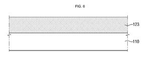
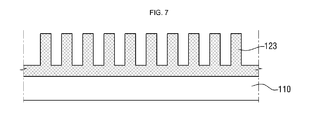
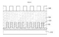
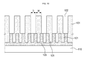
- FIGS. 6 through 10 are cross-sectional views illustrating steps of a method of manufacturing a color filter-integrated polarizer according to an embodiment of the present invention.
- a resin layer 123 may be formed on a substrate 110.
- the substrate 110 can be made of any material capable of transmitting visible light.
- the material that forms the substrate 110 may be selected according to the purpose of use or a process. Examples of the material may include various polymers such as, but not limited to, glass, quartz, acrylic, triacetylcellulose (TAC), cyclic olefin copolymer (COC), cyclic olefin polymer (COP), polycarbonate (PC), polyethylene naphthalate (PET), polyimide (PI), polyethylene naphthalate (PEN), polyether sulfone (PES), and polyarylate (PAR).
- the substrate 110 may also be made of an optical film having a certain degree of flexibility.
- the resin layer 123 can be made of any non-conductive material.
- the non-conductive material may have a refractive index of 1.0 to 1.3.
- the resin layer 123 may be patterned.
- the resin layer 123 can be patterned using any method that can form patterns of a desired nano size.
- the patterning method include, but are not limited to, nano-imprinting, photoresist, double patterning technology (DPT), and block copolymer (BCP) alignment patterning.
- a bottom portion of the patterned resin layer 123 may remain.
- conductive wire patterns 121 and a conductive material 124 may be formed on the entire surface of the patterned resin layer 123.
- the conductive wire patterns 121 may be formed in spaces of the patterned resin layer 123 using, but not limited to, long-throw sputtering, self-ionized sputtering or electroless plating having superior gap-filling characteristics.
- the upper surface of the conductive material 124 may not be even due to the effect of the patterned resin layer 123.
- the upper surface of the conductive material 124 may be planarized by etching or chemical mechanical polishing (CMP).
- CMP chemical mechanical polishing
- the present invention is not limited to these methods.
- the upper surface of the conductive material 124 may be planarized by repeating a deposition process and an etching process a number of times.
- mask patterns 140 may be formed on the conductive material 124.
- the mask patterns 140 may be formed using, but not limited to, nano-imprinting, photoresist, etc.
- a plurality of holes 122 may be formed by etching the conductive material 124 using the mask patterns 140.
- a plurality of holes having a predetermined size D1 and period (D1+W1) may be located adjacent to each other to form one group.
- a plurality of holes having a predetermined size D2 and period (D2+W2) which are different from those of the holes in the first region, may be located adjacent to each other to form one group.
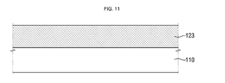
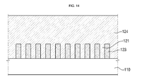
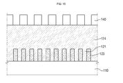
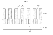
- FIGS. 11 through 17 are cross-sectional views illustrating a method of manufacturing a color filter-integrated polarizer according to another embodiment.
- a resin layer 123 may be formed on a substrate 110.
- the resin layer 123 can be made of any non-conductive material.
- the non-conductive material may have a refractive index of 1.0 to 1.3.
- the resin layer 123 may be patterned.
- the resin layer 123 can be patterned using any method that can form patterns of a desired nano size. Examples of the patterning method include, but are not limited to, nano-imprinting, photoresist, DPT, and BCP alignment patterning.
- the remaining bottom portion of the patterned resin layer 123 may be removed.
- the removal of the bottom portion may be achieved using, but not limited to, etching.
- conductive wire patterns 121 and a conductive material 124 may be formed on the entire surface of the substrate 110 and the patterned resin layer 123.
- the conductive wire patterns 121 may be formed in spaces of the patterned resin layer 123 using, but not limited to, long-throw sputtering, self-ionized sputtering or electroless plating having superior gap-filling characteristics.
- the upper surface of the conductive material 124 may not be even due to the effect of the patterned resin layer 123.
- the upper surface of the conductive material 124 may be planarized by etching or CMP.
- the present concept is not limited to these methods.
- the upper surface of the conductive material 124 may be planarized by repeating a deposition process and an etching process a number of times.
- mask patterns 140 may be formed on the conductive material 124.
- the mask patterns 140 may be formed using, but not limited to, nano-imprinting, photoresist, etc.
- a plurality of holes 122 may be formed by etching the conductive material 124 using the mask patterns 140.
- a plurality of holes having a predetermined size D3 and period (D3+W3) may be located adjacent to each other to form one group.
- a plurality of holes having a predetermined size D4 and period (D4+W4) which are different from those of the holes in the first region, may be located adjacent to each other to form one group.
- the patterned resin layer 123 located in a space between the conductive wire patterns 121 may be removed.
- the removal of the patterned resin layer 123 may be achieved by, but not limited to, wet etching using an etchant having an etch selectivity with respect to the conductive wire patterns 121 or an ashing process using a gas.
- FIGS. 11 through 17 are similar to those of FIGS. 6 through 10 , and a redundant description thereof is omitted.
- FIG. 18 is a partial perspective view of a color filter-integrated polarizer according to another embodiment of the present disclosure.
- the color filter-integrated polarizer may include a first group G1 of a plurality of adjacent holes 122a having a first size D5 and a first period (D5+W5), a second group G2 of a plurality of adjacent holes 122b having a second size D6 and a second period (D6+W6), and a third group G3 of a plurality of adjacent holes 122c having a third size D7 and a third period (D7+W7).
- the first group G1, the second group G2 and the third group G3 may transmit wavelengths corresponding to red, green and blue, respectively. These three primary colors of light may be combined to express various colors.
- a space between the first through third groups G1 through G3 may correspond to a non-aperture region (such as a wiring region or a TFT region) of a panel. Thus, conductive wire patterns may not be formed in the space.
- Each of the first through third groups G1 through G3 may correspond to a pixel or a subpixel of a display device.
- FIG. 18 Other elements of FIG. 18 are similar to those of FIG. 1 , and thus a redundant description thereof is omitted.
- a color filter-integrated polarizer provided in the present disclosure makes it possible to produce a thinner display device.
- a method of manufacturing a color filter-integrated polarizer with increased process efficiency can be provided.
Landscapes
- Physics & Mathematics (AREA)
- General Physics & Mathematics (AREA)
- Optics & Photonics (AREA)
- Nonlinear Science (AREA)
- Mathematical Physics (AREA)
- Chemical & Material Sciences (AREA)
- Crystallography & Structural Chemistry (AREA)
- Spectroscopy & Molecular Physics (AREA)
- Polarising Elements (AREA)
- Optical Filters (AREA)
Applications Claiming Priority (1)
| Application Number | Priority Date | Filing Date | Title |
|---|---|---|---|
| KR1020140162754A KR102259048B1 (ko) | 2014-11-20 | 2014-11-20 | 컬러 필터 일체형 편광자 및 이의 제조방법 |
Publications (2)
| Publication Number | Publication Date |
|---|---|
| EP3023833A1 true EP3023833A1 (fr) | 2016-05-25 |
| EP3023833B1 EP3023833B1 (fr) | 2018-10-10 |
Family
ID=53776492
Family Applications (1)
| Application Number | Title | Priority Date | Filing Date |
|---|---|---|---|
| EP15179831.1A Active EP3023833B1 (fr) | 2014-11-20 | 2015-08-05 | Polariseur à filtre intégré coloré et son procédé de fabrication |
Country Status (4)
| Country | Link |
|---|---|
| US (1) | US10317694B2 (fr) |
| EP (1) | EP3023833B1 (fr) |
| KR (1) | KR102259048B1 (fr) |
| CN (1) | CN105629554B (fr) |
Cited By (1)
| Publication number | Priority date | Publication date | Assignee | Title |
|---|---|---|---|---|
| CN109599030A (zh) * | 2017-09-30 | 2019-04-09 | 昆山国显光电有限公司 | 显示屏及电子产品 |
Families Citing this family (8)
| Publication number | Priority date | Publication date | Assignee | Title |
|---|---|---|---|---|
| WO2016191142A2 (fr) * | 2015-05-27 | 2016-12-01 | Verily Life Sciences Llc | Imageur nanophotonique hyperspectral/à superpixel de champ lumineux |
| KR102689225B1 (ko) | 2016-10-07 | 2024-07-29 | 삼성디스플레이 주식회사 | 표시 장치 및 이의 제조 방법 |
| WO2021157228A1 (fr) * | 2020-02-03 | 2021-08-12 | 富士フイルム株式会社 | Plaque de polarisation, plaque de polarisation circulaire, et procédé de fabrication de plaque de polarisation circulaire |
| CN112198705A (zh) * | 2020-10-26 | 2021-01-08 | 武汉华星光电技术有限公司 | 彩膜基板、阵列基板及显示面板 |
| CN113138490A (zh) * | 2021-04-23 | 2021-07-20 | 武汉华星光电技术有限公司 | 反射式显示面板 |
| US12571954B2 (en) * | 2021-06-01 | 2026-03-10 | Moxtek, Inc. | Optical device with a flexible, opaque-region |
| KR102723640B1 (ko) | 2022-05-03 | 2024-10-30 | 경북대학교 산학협력단 | 동축 구멍 디스크 배열 구조 기반 플라즈모닉 컬러필터 |
| CN115643773B (zh) * | 2022-10-18 | 2026-01-02 | 武汉天马微电子有限公司 | 一种显示面板和显示装置 |
Citations (5)
| Publication number | Priority date | Publication date | Assignee | Title |
|---|---|---|---|---|
| US20050275934A1 (en) * | 2004-06-10 | 2005-12-15 | Clemson University | Plasmon-photon coupled optical devices |
| US20080100779A1 (en) * | 2006-10-30 | 2008-05-01 | Dae Ho Choo | Method of forming an integrated optical polarization grid on an lcd subsrate and liquid crystal display manufactured to include the grid |
| US20110151605A1 (en) * | 2009-12-18 | 2011-06-23 | Min-Sung Yoon | Method for fabricating color filter using surface plasmon and method for fabricating liquid crystal display device |
| EP2523038A1 (fr) * | 2011-05-13 | 2012-11-14 | BOE Technology Group Co., Ltd. | Substrat de filtre de couleur capable de polarisation et son procédé de fabrication |
| US20140268332A1 (en) * | 2013-03-15 | 2014-09-18 | Sandia Corporation | Dye and pigment-free structural colors and angle-insensitive spectrum filters |
Family Cites Families (23)
| Publication number | Priority date | Publication date | Assignee | Title |
|---|---|---|---|---|
| US6040936A (en) * | 1998-10-08 | 2000-03-21 | Nec Research Institute, Inc. | Optical transmission control apparatus utilizing metal films perforated with subwavelength-diameter holes |
| US6285020B1 (en) * | 1999-11-05 | 2001-09-04 | Nec Research Institute, Inc. | Enhanced optical transmission apparatus with improved inter-surface coupling |
| JP4600013B2 (ja) | 2004-11-30 | 2010-12-15 | 住友化学株式会社 | 偏光分離機能を有するカラーフィルター及びそれを備える表示装置 |
| KR20070010472A (ko) * | 2005-07-19 | 2007-01-24 | 삼성전자주식회사 | 하이브리드형 편광자와, 이의 제조 방법 및 이를 갖는표시장치 |
| KR20070037864A (ko) * | 2005-10-04 | 2007-04-09 | 엘지.필립스 엘시디 주식회사 | 액정 표시패널과 그의 제조방법 |
| KR101340900B1 (ko) * | 2007-04-10 | 2013-12-13 | 삼성디스플레이 주식회사 | 이중층 구조의 와이어 그리드 편광자 및 그 제조 방법 |
| CN101943843B (zh) * | 2009-05-22 | 2012-03-07 | 上海丽恒光微电子科技有限公司 | 集成微型显示投影及成像系统 |
| KR101313654B1 (ko) * | 2009-12-18 | 2013-10-02 | 엘지디스플레이 주식회사 | 표면 플라즈몬을 이용한 컬러필터와 액정표시장치 및 그 제조방법 |
| KR101274591B1 (ko) | 2009-12-18 | 2013-06-13 | 엘지디스플레이 주식회사 | 표면 플라즈몬을 이용한 컬러필터와 액정표시장치 및 그 제조방법 |
| JP5517717B2 (ja) * | 2010-04-16 | 2014-06-11 | 株式会社ジャパンディスプレイ | 液晶表示装置 |
| KR20110120722A (ko) | 2010-04-29 | 2011-11-04 | 엘지디스플레이 주식회사 | 나노 패터닝 방법 및 이를 이용한 표면 플라즈몬 컬러필터와 액정표시장치의 제조방법 |
| KR101640818B1 (ko) * | 2010-04-29 | 2016-07-19 | 엘지디스플레이 주식회사 | 표면 플라즈몬을 이용한 편광 컬러필터 및 이를 구비한 액정표시장치 |
| EP2487530B1 (fr) * | 2011-02-14 | 2015-02-25 | Samsung Electronics Co., Ltd. | Panneau d'affichage comprenant un polariseur sélectif de couleur type à grille métallique |
| KR101282138B1 (ko) * | 2011-02-14 | 2013-07-04 | 삼성전자주식회사 | 디스플레이패널 및 이를 포함하는 디스플레이장치 |
| US8587751B2 (en) * | 2011-02-14 | 2013-11-19 | Samsung Electronics Co., Ltd. | Display panel and display apparatus having the same |
| KR101336097B1 (ko) * | 2012-05-11 | 2013-12-03 | 연세대학교 산학협력단 | 와이어 그리드 편광자를 구비하는 액정 디스플레이 장치 |
| KR101977061B1 (ko) | 2012-07-10 | 2019-05-13 | 삼성디스플레이 주식회사 | 편광 소자, 이를 포함하는 표시 패널 및 이의 제조 방법 |
| KR102116308B1 (ko) | 2013-09-04 | 2020-06-01 | 삼성디스플레이 주식회사 | 표시 장치 |
| KR20150029817A (ko) | 2013-09-10 | 2015-03-19 | 삼성디스플레이 주식회사 | 편광판, 이를 갖는 표시장치 및 이의 제조방법 |
| KR102079163B1 (ko) | 2013-10-02 | 2020-02-20 | 삼성디스플레이 주식회사 | 와이어 그리드 편광자, 이를 포함하는 표시 장치 및 이의 제조방법 |
| KR102132883B1 (ko) | 2013-12-10 | 2020-07-13 | 삼성디스플레이 주식회사 | 광추출 효율이 향상된 유기 발광 표시 장치 및 이의 제조 방법 |
| KR102150859B1 (ko) | 2014-01-13 | 2020-09-03 | 삼성디스플레이 주식회사 | 표시장치 |
| KR20150095971A (ko) | 2014-02-12 | 2015-08-24 | 삼성디스플레이 주식회사 | 마스터 몰드, 임프린트 몰드 및 임프린트 몰드를 이용하여 표시장치를 제조하는 방법 |
-
2014
- 2014-11-20 KR KR1020140162754A patent/KR102259048B1/ko active Active
-
2015
- 2015-06-01 US US14/727,186 patent/US10317694B2/en active Active
- 2015-08-05 EP EP15179831.1A patent/EP3023833B1/fr active Active
- 2015-10-23 CN CN201510695596.6A patent/CN105629554B/zh active Active
Patent Citations (5)
| Publication number | Priority date | Publication date | Assignee | Title |
|---|---|---|---|---|
| US20050275934A1 (en) * | 2004-06-10 | 2005-12-15 | Clemson University | Plasmon-photon coupled optical devices |
| US20080100779A1 (en) * | 2006-10-30 | 2008-05-01 | Dae Ho Choo | Method of forming an integrated optical polarization grid on an lcd subsrate and liquid crystal display manufactured to include the grid |
| US20110151605A1 (en) * | 2009-12-18 | 2011-06-23 | Min-Sung Yoon | Method for fabricating color filter using surface plasmon and method for fabricating liquid crystal display device |
| EP2523038A1 (fr) * | 2011-05-13 | 2012-11-14 | BOE Technology Group Co., Ltd. | Substrat de filtre de couleur capable de polarisation et son procédé de fabrication |
| US20140268332A1 (en) * | 2013-03-15 | 2014-09-18 | Sandia Corporation | Dye and pigment-free structural colors and angle-insensitive spectrum filters |
Cited By (1)
| Publication number | Priority date | Publication date | Assignee | Title |
|---|---|---|---|---|
| CN109599030A (zh) * | 2017-09-30 | 2019-04-09 | 昆山国显光电有限公司 | 显示屏及电子产品 |
Also Published As
| Publication number | Publication date |
|---|---|
| CN105629554B (zh) | 2021-06-08 |
| US10317694B2 (en) | 2019-06-11 |
| CN105629554A (zh) | 2016-06-01 |
| KR102259048B1 (ko) | 2021-06-03 |
| KR20160060859A (ko) | 2016-05-31 |
| EP3023833B1 (fr) | 2018-10-10 |
| US20160147080A1 (en) | 2016-05-26 |
Similar Documents
| Publication | Publication Date | Title |
|---|---|---|
| EP3023833B1 (fr) | Polariseur à filtre intégré coloré et son procédé de fabrication | |
| KR102305200B1 (ko) | 와이어 그리드 편광자, 이를 포함하는 표시 장치 및 이의 제조방법 | |
| US10295717B2 (en) | Wire grid polarizing plate, display device including the same, and method of fabricating said display device | |
| EP3023821A1 (fr) | Polariseur en grille metallique, dispositif d'affichage le comprenant et son procédé de fabrication | |
| US9488764B2 (en) | Wire grid polarizer and backlight unit using the same | |
| US20160033701A1 (en) | Wire grid polarizer and method of fabricating the same | |
| JP2012027492A (ja) | 液晶表示装置 | |
| CN105700056A (zh) | 偏振板、包括该偏振板的tft基板及制造该偏振板的方法 | |
| KR102079163B1 (ko) | 와이어 그리드 편광자, 이를 포함하는 표시 장치 및 이의 제조방법 | |
| US20160077377A1 (en) | Wire grid polarizer, display device including the same and method for fabricating the same | |
| KR102241418B1 (ko) | 와이어 그리드 편광자 및 이의 제조방법 | |
| KR102133211B1 (ko) | 와이어 그리드 편광자의 제조방법 | |
| US20160266294A1 (en) | Wire grid polarizer and method of fabricating the same | |
| JP2010251201A (ja) | 導光板、面発光装置および表示装置 | |
| CN119053910A (zh) | 发光器件及其制备方法、背光模组、显示基板、显示装置 | |
| CN115643773A (zh) | 一种显示面板和显示装置 |
Legal Events
| Date | Code | Title | Description |
|---|---|---|---|
| 17P | Request for examination filed |
Effective date: 20160304 |
|
| AK | Designated contracting states |
Kind code of ref document: A1 Designated state(s): AL AT BE BG CH CY CZ DE DK EE ES FI FR GB GR HR HU IE IS IT LI LT LU LV MC MK MT NL NO PL PT RO RS SE SI SK SM TR |
|
| AX | Request for extension of the european patent |
Extension state: BA ME |
|
| PUAI | Public reference made under article 153(3) epc to a published international application that has entered the european phase |
Free format text: ORIGINAL CODE: 0009012 |
|
| GRAP | Despatch of communication of intention to grant a patent |
Free format text: ORIGINAL CODE: EPIDOSNIGR1 |
|
| STAA | Information on the status of an ep patent application or granted ep patent |
Free format text: STATUS: GRANT OF PATENT IS INTENDED |
|
| INTG | Intention to grant announced |
Effective date: 20180511 |
|
| GRAJ | Information related to disapproval of communication of intention to grant by the applicant or resumption of examination proceedings by the epo deleted |
Free format text: ORIGINAL CODE: EPIDOSDIGR1 |
|
| STAA | Information on the status of an ep patent application or granted ep patent |
Free format text: STATUS: REQUEST FOR EXAMINATION WAS MADE |
|
| GRAR | Information related to intention to grant a patent recorded |
Free format text: ORIGINAL CODE: EPIDOSNIGR71 |
|
| GRAS | Grant fee paid |
Free format text: ORIGINAL CODE: EPIDOSNIGR3 |
|
| STAA | Information on the status of an ep patent application or granted ep patent |
Free format text: STATUS: GRANT OF PATENT IS INTENDED |
|
| INTC | Intention to grant announced (deleted) | ||
| INTG | Intention to grant announced |
Effective date: 20180726 |
|
| GRAA | (expected) grant |
Free format text: ORIGINAL CODE: 0009210 |
|
| STAA | Information on the status of an ep patent application or granted ep patent |
Free format text: STATUS: THE PATENT HAS BEEN GRANTED |
|
| AK | Designated contracting states |
Kind code of ref document: B1 Designated state(s): AL AT BE BG CH CY CZ DE DK EE ES FI FR GB GR HR HU IE IS IT LI LT LU LV MC MK MT NL NO PL PT RO RS SE SI SK SM TR |
|
| REG | Reference to a national code |
Ref country code: GB Ref legal event code: FG4D |
|
| REG | Reference to a national code |
Ref country code: AT Ref legal event code: REF Ref document number: 1051933 Country of ref document: AT Kind code of ref document: T Effective date: 20181015 Ref country code: CH Ref legal event code: EP |
|
| REG | Reference to a national code |
Ref country code: DE Ref legal event code: R096 Ref document number: 602015017743 Country of ref document: DE Ref country code: IE Ref legal event code: FG4D |
|
| REG | Reference to a national code |
Ref country code: NL Ref legal event code: FP |
|
| REG | Reference to a national code |
Ref country code: LT Ref legal event code: MG4D |
|
| REG | Reference to a national code |
Ref country code: AT Ref legal event code: MK05 Ref document number: 1051933 Country of ref document: AT Kind code of ref document: T Effective date: 20181010 |
|
| PG25 | Lapsed in a contracting state [announced via postgrant information from national office to epo] |
Ref country code: HR Free format text: LAPSE BECAUSE OF FAILURE TO SUBMIT A TRANSLATION OF THE DESCRIPTION OR TO PAY THE FEE WITHIN THE PRESCRIBED TIME-LIMIT Effective date: 20181010 Ref country code: PL Free format text: LAPSE BECAUSE OF FAILURE TO SUBMIT A TRANSLATION OF THE DESCRIPTION OR TO PAY THE FEE WITHIN THE PRESCRIBED TIME-LIMIT Effective date: 20181010 Ref country code: LV Free format text: LAPSE BECAUSE OF FAILURE TO SUBMIT A TRANSLATION OF THE DESCRIPTION OR TO PAY THE FEE WITHIN THE PRESCRIBED TIME-LIMIT Effective date: 20181010 Ref country code: FI Free format text: LAPSE BECAUSE OF FAILURE TO SUBMIT A TRANSLATION OF THE DESCRIPTION OR TO PAY THE FEE WITHIN THE PRESCRIBED TIME-LIMIT Effective date: 20181010 Ref country code: LT Free format text: LAPSE BECAUSE OF FAILURE TO SUBMIT A TRANSLATION OF THE DESCRIPTION OR TO PAY THE FEE WITHIN THE PRESCRIBED TIME-LIMIT Effective date: 20181010 Ref country code: BG Free format text: LAPSE BECAUSE OF FAILURE TO SUBMIT A TRANSLATION OF THE DESCRIPTION OR TO PAY THE FEE WITHIN THE PRESCRIBED TIME-LIMIT Effective date: 20190110 Ref country code: IS Free format text: LAPSE BECAUSE OF FAILURE TO SUBMIT A TRANSLATION OF THE DESCRIPTION OR TO PAY THE FEE WITHIN THE PRESCRIBED TIME-LIMIT Effective date: 20190210 Ref country code: AT Free format text: LAPSE BECAUSE OF FAILURE TO SUBMIT A TRANSLATION OF THE DESCRIPTION OR TO PAY THE FEE WITHIN THE PRESCRIBED TIME-LIMIT Effective date: 20181010 Ref country code: NO Free format text: LAPSE BECAUSE OF FAILURE TO SUBMIT A TRANSLATION OF THE DESCRIPTION OR TO PAY THE FEE WITHIN THE PRESCRIBED TIME-LIMIT Effective date: 20190110 Ref country code: ES Free format text: LAPSE BECAUSE OF FAILURE TO SUBMIT A TRANSLATION OF THE DESCRIPTION OR TO PAY THE FEE WITHIN THE PRESCRIBED TIME-LIMIT Effective date: 20181010 |
|
| PG25 | Lapsed in a contracting state [announced via postgrant information from national office to epo] |
Ref country code: GR Free format text: LAPSE BECAUSE OF FAILURE TO SUBMIT A TRANSLATION OF THE DESCRIPTION OR TO PAY THE FEE WITHIN THE PRESCRIBED TIME-LIMIT Effective date: 20190111 Ref country code: PT Free format text: LAPSE BECAUSE OF FAILURE TO SUBMIT A TRANSLATION OF THE DESCRIPTION OR TO PAY THE FEE WITHIN THE PRESCRIBED TIME-LIMIT Effective date: 20190210 Ref country code: AL Free format text: LAPSE BECAUSE OF FAILURE TO SUBMIT A TRANSLATION OF THE DESCRIPTION OR TO PAY THE FEE WITHIN THE PRESCRIBED TIME-LIMIT Effective date: 20181010 Ref country code: RS Free format text: LAPSE BECAUSE OF FAILURE TO SUBMIT A TRANSLATION OF THE DESCRIPTION OR TO PAY THE FEE WITHIN THE PRESCRIBED TIME-LIMIT Effective date: 20181010 Ref country code: SE Free format text: LAPSE BECAUSE OF FAILURE TO SUBMIT A TRANSLATION OF THE DESCRIPTION OR TO PAY THE FEE WITHIN THE PRESCRIBED TIME-LIMIT Effective date: 20181010 |
|
| REG | Reference to a national code |
Ref country code: DE Ref legal event code: R097 Ref document number: 602015017743 Country of ref document: DE |
|
| PG25 | Lapsed in a contracting state [announced via postgrant information from national office to epo] |
Ref country code: IT Free format text: LAPSE BECAUSE OF FAILURE TO SUBMIT A TRANSLATION OF THE DESCRIPTION OR TO PAY THE FEE WITHIN THE PRESCRIBED TIME-LIMIT Effective date: 20181010 Ref country code: DK Free format text: LAPSE BECAUSE OF FAILURE TO SUBMIT A TRANSLATION OF THE DESCRIPTION OR TO PAY THE FEE WITHIN THE PRESCRIBED TIME-LIMIT Effective date: 20181010 Ref country code: CZ Free format text: LAPSE BECAUSE OF FAILURE TO SUBMIT A TRANSLATION OF THE DESCRIPTION OR TO PAY THE FEE WITHIN THE PRESCRIBED TIME-LIMIT Effective date: 20181010 |
|
| PLBE | No opposition filed within time limit |
Free format text: ORIGINAL CODE: 0009261 |
|
| STAA | Information on the status of an ep patent application or granted ep patent |
Free format text: STATUS: NO OPPOSITION FILED WITHIN TIME LIMIT |
|
| PG25 | Lapsed in a contracting state [announced via postgrant information from national office to epo] |
Ref country code: EE Free format text: LAPSE BECAUSE OF FAILURE TO SUBMIT A TRANSLATION OF THE DESCRIPTION OR TO PAY THE FEE WITHIN THE PRESCRIBED TIME-LIMIT Effective date: 20181010 Ref country code: SM Free format text: LAPSE BECAUSE OF FAILURE TO SUBMIT A TRANSLATION OF THE DESCRIPTION OR TO PAY THE FEE WITHIN THE PRESCRIBED TIME-LIMIT Effective date: 20181010 Ref country code: RO Free format text: LAPSE BECAUSE OF FAILURE TO SUBMIT A TRANSLATION OF THE DESCRIPTION OR TO PAY THE FEE WITHIN THE PRESCRIBED TIME-LIMIT Effective date: 20181010 Ref country code: SK Free format text: LAPSE BECAUSE OF FAILURE TO SUBMIT A TRANSLATION OF THE DESCRIPTION OR TO PAY THE FEE WITHIN THE PRESCRIBED TIME-LIMIT Effective date: 20181010 |
|
| 26N | No opposition filed |
Effective date: 20190711 |
|
| PG25 | Lapsed in a contracting state [announced via postgrant information from national office to epo] |
Ref country code: SI Free format text: LAPSE BECAUSE OF FAILURE TO SUBMIT A TRANSLATION OF THE DESCRIPTION OR TO PAY THE FEE WITHIN THE PRESCRIBED TIME-LIMIT Effective date: 20181010 |
|
| PG25 | Lapsed in a contracting state [announced via postgrant information from national office to epo] |
Ref country code: TR Free format text: LAPSE BECAUSE OF FAILURE TO SUBMIT A TRANSLATION OF THE DESCRIPTION OR TO PAY THE FEE WITHIN THE PRESCRIBED TIME-LIMIT Effective date: 20181010 |
|
| PG25 | Lapsed in a contracting state [announced via postgrant information from national office to epo] |
Ref country code: MC Free format text: LAPSE BECAUSE OF FAILURE TO SUBMIT A TRANSLATION OF THE DESCRIPTION OR TO PAY THE FEE WITHIN THE PRESCRIBED TIME-LIMIT Effective date: 20181010 Ref country code: CH Free format text: LAPSE BECAUSE OF NON-PAYMENT OF DUE FEES Effective date: 20190831 Ref country code: LI Free format text: LAPSE BECAUSE OF NON-PAYMENT OF DUE FEES Effective date: 20190831 Ref country code: LU Free format text: LAPSE BECAUSE OF NON-PAYMENT OF DUE FEES Effective date: 20190805 |
|
| REG | Reference to a national code |
Ref country code: BE Ref legal event code: MM Effective date: 20190831 |
|
| PG25 | Lapsed in a contracting state [announced via postgrant information from national office to epo] |
Ref country code: IE Free format text: LAPSE BECAUSE OF NON-PAYMENT OF DUE FEES Effective date: 20190805 |
|
| PG25 | Lapsed in a contracting state [announced via postgrant information from national office to epo] |
Ref country code: BE Free format text: LAPSE BECAUSE OF NON-PAYMENT OF DUE FEES Effective date: 20190831 |
|
| PG25 | Lapsed in a contracting state [announced via postgrant information from national office to epo] |
Ref country code: CY Free format text: LAPSE BECAUSE OF FAILURE TO SUBMIT A TRANSLATION OF THE DESCRIPTION OR TO PAY THE FEE WITHIN THE PRESCRIBED TIME-LIMIT Effective date: 20181010 |
|
| PG25 | Lapsed in a contracting state [announced via postgrant information from national office to epo] |
Ref country code: HU Free format text: LAPSE BECAUSE OF FAILURE TO SUBMIT A TRANSLATION OF THE DESCRIPTION OR TO PAY THE FEE WITHIN THE PRESCRIBED TIME-LIMIT; INVALID AB INITIO Effective date: 20150805 Ref country code: MT Free format text: LAPSE BECAUSE OF FAILURE TO SUBMIT A TRANSLATION OF THE DESCRIPTION OR TO PAY THE FEE WITHIN THE PRESCRIBED TIME-LIMIT Effective date: 20181010 |
|
| PG25 | Lapsed in a contracting state [announced via postgrant information from national office to epo] |
Ref country code: MK Free format text: LAPSE BECAUSE OF FAILURE TO SUBMIT A TRANSLATION OF THE DESCRIPTION OR TO PAY THE FEE WITHIN THE PRESCRIBED TIME-LIMIT Effective date: 20181010 |
|
| P01 | Opt-out of the competence of the unified patent court (upc) registered |
Effective date: 20230515 |
|
| PGFP | Annual fee paid to national office [announced via postgrant information from national office to epo] |
Ref country code: NL Payment date: 20250722 Year of fee payment: 11 |
|
| PGFP | Annual fee paid to national office [announced via postgrant information from national office to epo] |
Ref country code: DE Payment date: 20250721 Year of fee payment: 11 |
|
| PGFP | Annual fee paid to national office [announced via postgrant information from national office to epo] |
Ref country code: GB Payment date: 20250722 Year of fee payment: 11 |
|
| PGFP | Annual fee paid to national office [announced via postgrant information from national office to epo] |
Ref country code: FR Payment date: 20250725 Year of fee payment: 11 |