EP3033652B1 - Impression de motif de feuille - Google Patents
Impression de motif de feuille Download PDFInfo
- Publication number
- EP3033652B1 EP3033652B1 EP13891464.3A EP13891464A EP3033652B1 EP 3033652 B1 EP3033652 B1 EP 3033652B1 EP 13891464 A EP13891464 A EP 13891464A EP 3033652 B1 EP3033652 B1 EP 3033652B1
- Authority
- EP
- European Patent Office
- Prior art keywords
- intermediate transfer
- layer
- transfer member
- foil
- examples
- Prior art date
- Legal status (The legal status is an assumption and is not a legal conclusion. Google has not performed a legal analysis and makes no representation as to the accuracy of the status listed.)
- Active
Links
- 239000011888 foil Substances 0.000 title claims description 137
- 239000010410 layer Substances 0.000 claims description 181
- 238000012546 transfer Methods 0.000 claims description 115
- 239000000758 substrate Substances 0.000 claims description 47
- 238000000034 method Methods 0.000 claims description 29
- 239000003550 marker Substances 0.000 claims description 14
- 230000015572 biosynthetic process Effects 0.000 claims description 10
- 239000007788 liquid Substances 0.000 claims description 9
- 238000005096 rolling process Methods 0.000 claims description 6
- 239000002245 particle Substances 0.000 claims description 3
- 239000012790 adhesive layer Substances 0.000 claims 2
- 239000000976 ink Substances 0.000 description 90
- 239000011247 coating layer Substances 0.000 description 13
- 238000010586 diagram Methods 0.000 description 12
- 238000003384 imaging method Methods 0.000 description 11
- 230000015654 memory Effects 0.000 description 8
- 230000001070 adhesive effect Effects 0.000 description 7
- 230000008569 process Effects 0.000 description 7
- 239000000853 adhesive Substances 0.000 description 6
- 230000007246 mechanism Effects 0.000 description 5
- 229910052751 metal Inorganic materials 0.000 description 4
- 238000003860 storage Methods 0.000 description 4
- 238000010438 heat treatment Methods 0.000 description 3
- 239000000463 material Substances 0.000 description 3
- 230000009471 action Effects 0.000 description 2
- 239000004020 conductor Substances 0.000 description 2
- 230000006870 function Effects 0.000 description 2
- 238000004519 manufacturing process Methods 0.000 description 2
- 230000004913 activation Effects 0.000 description 1
- 230000006978 adaptation Effects 0.000 description 1
- 238000004891 communication Methods 0.000 description 1
- 230000000694 effects Effects 0.000 description 1
- 230000009477 glass transition Effects 0.000 description 1
- 238000010348 incorporation Methods 0.000 description 1
- 238000002844 melting Methods 0.000 description 1
- 230000008018 melting Effects 0.000 description 1
- 230000002085 persistent effect Effects 0.000 description 1
- 238000002360 preparation method Methods 0.000 description 1
- 238000003825 pressing Methods 0.000 description 1
- 238000012545 processing Methods 0.000 description 1
- 230000004044 response Effects 0.000 description 1
- 238000000926 separation method Methods 0.000 description 1
- 238000010008 shearing Methods 0.000 description 1
- 239000002356 single layer Substances 0.000 description 1
- 230000032258 transport Effects 0.000 description 1
Images


Classifications
-
- G—PHYSICS
- G03—PHOTOGRAPHY; CINEMATOGRAPHY; ANALOGOUS TECHNIQUES USING WAVES OTHER THAN OPTICAL WAVES; ELECTROGRAPHY; HOLOGRAPHY
- G03G—ELECTROGRAPHY; ELECTROPHOTOGRAPHY; MAGNETOGRAPHY
- G03G15/00—Apparatus for electrographic processes using a charge pattern
- G03G15/14—Apparatus for electrographic processes using a charge pattern for transferring a pattern to a second base
- G03G15/16—Apparatus for electrographic processes using a charge pattern for transferring a pattern to a second base of a toner pattern, e.g. a powder pattern, e.g. magnetic transfer
- G03G15/1605—Apparatus for electrographic processes using a charge pattern for transferring a pattern to a second base of a toner pattern, e.g. a powder pattern, e.g. magnetic transfer using at least one intermediate support
-
- G—PHYSICS
- G03—PHOTOGRAPHY; CINEMATOGRAPHY; ANALOGOUS TECHNIQUES USING WAVES OTHER THAN OPTICAL WAVES; ELECTROGRAPHY; HOLOGRAPHY
- G03G—ELECTROGRAPHY; ELECTROPHOTOGRAPHY; MAGNETOGRAPHY
- G03G15/00—Apparatus for electrographic processes using a charge pattern
- G03G15/01—Apparatus for electrographic processes using a charge pattern for producing multicoloured copies
- G03G15/0105—Details of unit
- G03G15/0131—Details of unit for transferring a pattern to a second base
-
- G—PHYSICS
- G03—PHOTOGRAPHY; CINEMATOGRAPHY; ANALOGOUS TECHNIQUES USING WAVES OTHER THAN OPTICAL WAVES; ELECTROGRAPHY; HOLOGRAPHY
- G03G—ELECTROGRAPHY; ELECTROPHOTOGRAPHY; MAGNETOGRAPHY
- G03G15/00—Apparatus for electrographic processes using a charge pattern
- G03G15/01—Apparatus for electrographic processes using a charge pattern for producing multicoloured copies
- G03G15/0142—Structure of complete machines
- G03G15/0178—Structure of complete machines using more than one reusable electrographic recording member, e.g. one for every monocolour image
- G03G15/0189—Structure of complete machines using more than one reusable electrographic recording member, e.g. one for every monocolour image primary transfer to an intermediate transfer belt
-
- G—PHYSICS
- G03—PHOTOGRAPHY; CINEMATOGRAPHY; ANALOGOUS TECHNIQUES USING WAVES OTHER THAN OPTICAL WAVES; ELECTROGRAPHY; HOLOGRAPHY
- G03G—ELECTROGRAPHY; ELECTROPHOTOGRAPHY; MAGNETOGRAPHY
- G03G15/00—Apparatus for electrographic processes using a charge pattern
- G03G15/06—Apparatus for electrographic processes using a charge pattern for developing
- G03G15/10—Apparatus for electrographic processes using a charge pattern for developing using a liquid developer
-
- G—PHYSICS
- G03—PHOTOGRAPHY; CINEMATOGRAPHY; ANALOGOUS TECHNIQUES USING WAVES OTHER THAN OPTICAL WAVES; ELECTROGRAPHY; HOLOGRAPHY
- G03G—ELECTROGRAPHY; ELECTROPHOTOGRAPHY; MAGNETOGRAPHY
- G03G15/00—Apparatus for electrographic processes using a charge pattern
- G03G15/22—Apparatus for electrographic processes using a charge pattern involving the combination of more than one step according to groups G03G13/02 - G03G13/20
- G03G15/225—Apparatus for electrographic processes using a charge pattern involving the combination of more than one step according to groups G03G13/02 - G03G13/20 using contact-printing
-
- G—PHYSICS
- G03—PHOTOGRAPHY; CINEMATOGRAPHY; ANALOGOUS TECHNIQUES USING WAVES OTHER THAN OPTICAL WAVES; ELECTROGRAPHY; HOLOGRAPHY
- G03G—ELECTROGRAPHY; ELECTROPHOTOGRAPHY; MAGNETOGRAPHY
- G03G15/00—Apparatus for electrographic processes using a charge pattern
- G03G15/65—Apparatus which relate to the handling of copy material
- G03G15/6582—Special processing for irreversibly adding or changing the sheet copy material characteristics or its appearance, e.g. stamping, annotation printing, punching
- G03G15/6585—Special processing for irreversibly adding or changing the sheet copy material characteristics or its appearance, e.g. stamping, annotation printing, punching by using non-standard toners, e.g. transparent toner, gloss adding devices
-
- G—PHYSICS
- G03—PHOTOGRAPHY; CINEMATOGRAPHY; ANALOGOUS TECHNIQUES USING WAVES OTHER THAN OPTICAL WAVES; ELECTROGRAPHY; HOLOGRAPHY
- G03G—ELECTROGRAPHY; ELECTROPHOTOGRAPHY; MAGNETOGRAPHY
- G03G2215/00—Apparatus for electrophotographic processes
- G03G2215/00362—Apparatus for electrophotographic processes relating to the copy medium handling
- G03G2215/00443—Copy medium
- G03G2215/00493—Plastic
- G03G2215/00502—Transparent film
Definitions
- a first ink layer is first imaged according to a desired pattern on the photoconductor member and transferred onto the intermediate transfer member. Thereafter, by contacting a top coating layer of an unpatterned sheet of a foil assembly against the first ink layer (during rotation of the intermediate transfer member), select portions of the foil assembly become adhered to the first ink layer while other portions of the foil assembly do not become adhered to the first ink layer. Instead, these other portions remain positioned on the supply sheet of foil assembly and do not become part of the printed product. Typically, they are discarded or recycled separately from the printing process in the examples of the present disclosure.
- foil portions printed onto a substrate are hidden from view because they underlie at least one opaque ink layer.
- hidden foil portions are usable for advertising, transactional, security purposes, etc.
- foil printed portions serve as holographic components used in fraud and counterfeit protection solutions.
- Figure 2 is a side view of a printed product 40, according to one example of the present disclosure.
- printed product 40 is produced via printer 20 and/or one of the printers described later in examples of the present disclosure.
- the printed product 40 includes a foil layer 54.
- foil layer 54 comprises a metallic conductive material while in some examples, foil layer 54 need not be conductive but has a metallic appearance. In some examples, the foil layer 54 is conductive but does not necessarily have a metallic appearance.
- layers 50-58 as shown in Figure 2 are exaggerated (relative to the thickness of substrate 44) for illustrative purposes and do not necessarily represent a true scale of thicknesses of layers 50-58 relative to each other or relative to the substrate.
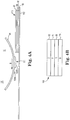
- printer 70 includes a feed station 97 to feed a substrate and/or other elements, such as a sheet of foil assembly or conductive elements to interact with intermediate transfer member 90 as part of forming a printed product according to at least some examples of the present disclosure.
- feed station 97 includes at least substantially the same features and attributes as feed station 24 ( Fig. 1 ).
- impression member 92 is selectively movable relative to (i.e. toward or away from) intermediate transfer member 90 (as represented by directional arrow S in Fig. 3 ) to enable selective rolling engagement of the impression member 92 against the intermediate transfer member 90.
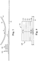
- the top coating layer 52 of the foil assembly 110 becomes adhered to portions 120A, 120B of the first patterned ink layer 121, and as intermediate transfer member 90 continues to rotate away from carrier 112 (per directional arrow B), portions 130A, 130B of foil assembly 110 separate from the remaining portions 132A, 132B, 132C of foil assembly 110 that remain on carrier 112.
- the foil layer (F) 54 comprises a conductive element and is concealed via providing first ink layer 121 ( Fig. 7B ) as an opaque color and/or material.
- the opaque color is white or a color generally matching the surface color of the final substrate 141.
- the at least one ink layer (which overlies the at least partially metallic border 204) is transparent or translucent to permit visibility of the metallic element through the overlying ink layer.
- the overlying ink layer is transparent or translucent and further includes color tinting to further enhance desired appearance characteristics of the metallic element defining border 204 or other feature.
- controller 412 of control portion 410 comprises at least one processor 413 and associated memories that are in communication with memory 414 to generate control signals directing operation of at least some components of the systems and components described throughout the present disclosure.
- these generated control signals include, but are not limited to, digitally printing foil patterns.
- a control portion 410 is present in the printer 20, 70, 370 of Figures 1, 2 , or 11 , respectively, at which layers of ink are printed in patterns on an intermediate transfer member to capture a foil portion having a matching pattern and then transferring the compilation of ink layers and foil portion onto a substrate.
- the control portion 410 controls the timing and sequence of printing of the ink layers relative to engagement with foil portions at the intermediate transfer member.
- method 500 includes digitally forming a first ink layer in a pattern on a photoconductor member and transferring the first ink layer onto an intermediate transfer member. As shown at 504, method 500 includes contacting a foil assembly against the first ink layer on the intermediate transfer member to cause select portions of the foil assembly to become adhered to the first ink layer.
- the patterned portion (i.e. the adhered portions) of the foil assembly has a shape matching the pattern of the first ink layer.
- the foil assembly includes a multi-layer assembly including a foil layer sandwiched between other layers, such as a release layer and coating layer, and may include a backing layer against the release layer.
Landscapes
- Physics & Mathematics (AREA)
- General Physics & Mathematics (AREA)
- Printing Methods (AREA)
- Decoration By Transfer Pictures (AREA)
Claims (12)
- Imprimante électrophotographique liquide (20) comprenant :une partie de formation d'image (22) pour transférer des première et seconde couches d'encre à motifs formées sur un élément photoconducteur (30) sur un élément de transfert intermédiaire (32), dans laquelle la seconde couche d'encre (58) couvre au moins une zone de la première couche d'encre à motifs (50) ;une partie d'alimentation (24) pour diriger une partie d'une couche de feuille conductrice (54) pour qu'elle adhère, selon le motif, sur la première couche d'encre (50) sur l'élément de transfert intermédiaire (32) avant que la seconde couche d'encre (58) soit transférée sur la partie de feuille et y adhère conformément au motif ; etune partie de transfert (26) pour amener le transfert de la partie de feuille conductrice de l'élément de transfert intermédiaire (32), par l'intermédiaire du transfert d'au moins la seconde couche d'encre (58) de l'élément de transfert intermédiaire (32), sur un substrat.
- Imprimante selon la revendication 1, comprenant :
une partie de commande (410) pour commander le fonctionnement de la partie de formation d'image (22) et le positionnement de l'élément de transfert intermédiaire (32) pour amener le transfert de la première couche d'encre à motifs vers l'élément de transfert intermédiaire (32) avant la formation de la seconde couche d'encre à motifs sur l'élément photoconducteur (30). - Imprimante selon la revendication 2, dans laquelle la partie d'alimentation (24) comporte une fourniture d'un ensemble de feuille conductrice comportant une couche de protection, une couche de libération, la couche de feuille conductrice et une couche adhésive du dessus, dans laquelle la partie d'alimentation (24) délivre la couche adhésive du dessus de l'ensemble de feuille conductrice en contact avec la première couche d'encre à motifs sur l'élément de transfert intermédiaire (32) pour amener la couche de libération de l'ensemble de feuille conductrice à définir une couche supérieure de l'ensemble de feuille conductrice lorsqu'elle se trouve sur l'élément de transfert intermédiaire (32).
- Imprimante selon la revendication 3, dans laquelle la partie de commande (410) commande la synchronisation de l'élément photoconducteur (30) pour amener la formation de la seconde couche à motifs et son transfert vers l'élément de transfert intermédiaire (32) au-dessus de la couche de libération sur l'élément de transfert intermédiaire (32), la seconde couche à motifs définissant la couche supérieure d'une compilation de couches formées sur l'élément de transfert intermédiaire (32).
- Imprimante selon la revendication 1, dans laquelle la partie de formation d'image (22) comprend l'élément photoconducteur (30), une station de charge (82), une station d'exposition à la lumière, une station de développement d'encre, et dans laquelle l'élément de transfert intermédiaire (32) peut être en prise par roulement contre l'élément photoconducteur, et forme un premier pincement, par rapport à l'élément photoconducteur (30).
- Imprimante selon la revendication 5, dans laquelle la partie de transfert comporte un élément d'impression (92) devant être en prise par roulement sélectif contre, et former un second pincement par rapport à, l'élément de transfert intermédiaire (32), et dans laquelle la partie d'alimentation (24) comporte une station positionnée de manière adjacente au second pincement pour alimenter une planche d'ensemble de feuille comportant le fait que la couche de feuille conductrice (54) devienne adhésive par rapport à la première couche d'encre (50) sur l'élément de transfert intermédiaire (32), dans laquelle l'élément d'impression (92) est espacé de l'élément de transfert intermédiaire (32) lorsque la planche de l'ensemble de feuille est mise en prise avec la première couche d'encre (50) sur l'élément de transfert intermédiaire (32).
- Imprimante selon la revendication 1, dans laquelle le substrat comprend une nappe généralement continue, et dans laquelle la partie d'alimentation (24) est positionnée de manière adjacente à l'élément de transfert intermédiaire (32) et interposée entre l'élément photoconducteur (30).
- Procédé d'impression :formant numériquement une première couche d'agent de marquage selon un motif sur un élément photoconducteur (30) et transférant la première couche d'agent de marquage sur un élément de transfert intermédiaire (32) ;mettant en contact un ensemble de feuille sans motif contre la première couche d'agent de marquage sur l'élément de transfert intermédiaire (32) pour amener une partie de l'ensemble de feuille à devenir adhésive à la première couche d'agent de marquage, la partie adhésive de l'ensemble de feuille définissant une partie à motifs ayant une forme correspondant au motif de la première couche d'agent de marquage ;formant numériquement une seconde couche d'agent de marquage, sur l'élément photoconducteur (30), couvrant au moins une zone du même motif que la première couche d'agent de marquage et transférant la seconde couche d'agent de marquage de l'élément photoconducteur (30) pour devenir adhésive sur au moins la partie à motifs de l'ensemble de feuille sur l'élément de transfert intermédiaire (32) ; ettransférant au moins la partie à motifs de l'ensemble de feuille, par l'intermédiaire d'un contact par roulement de la seconde couche d'agent de marquage sur l'élément de transfert intermédiaire (32) contre un substrat, sur le substrat.
- Procédé selon la revendication 8, dans lequel le substrat comprend une seule planche et dans lequel la mise en contact d'un ensemble de feuille comprend :
l'alimentation de l'ensemble de feuille au niveau d'un pincement de l'élément de transfert intermédiaire (32) et d'un élément d'impression (92) pour produire une compilation formée de la première couche d'agent de marquage et d'une couche de feuille à motifs de l'ensemble de feuille sur l'élément de transfert intermédiaire (32), dans lequel l'alimentation de l'ensemble de feuille est effectuée avant de former numériquement la seconde couche d'agent de marquage. - Procédé selon la revendication 8, dans lequel le substrat comprend une nappe et dans lequel la mise en contact de la planche de feuille comprend :
l'alimentation de l'élément de feuille d'un ensemble d'alimentation par rouleau qui peut entrer en prise de manière amovible contre l'élément de transfert intermédiaire (32) adjacent à un pincement entre l'élément de transfert intermédiaire (32) et l'élément photoconducteur (30). - Procédé selon la revendication 10, dans lequel l'emplacement est interposé entre l'élément photoconducteur (30) et un élément chauffant (95) pour appliquer de la chaleur sur les couches à motifs respectives sur l'élément de transfert intermédiaire (32).
- Procédé selon la revendication 8, dans lequel l'agent de marquage comprend une encre comprenant des particules pigmentées chargées dans un vecteur liquide et l'impression est effectuée par l'intermédiaire d'électrophotographie liquide.
Applications Claiming Priority (1)
| Application Number | Priority Date | Filing Date | Title |
|---|---|---|---|
| PCT/US2013/054710 WO2015023262A1 (fr) | 2013-08-13 | 2013-08-13 | Impression de motif de feuille |
Publications (3)
| Publication Number | Publication Date |
|---|---|
| EP3033652A1 EP3033652A1 (fr) | 2016-06-22 |
| EP3033652A4 EP3033652A4 (fr) | 2017-03-22 |
| EP3033652B1 true EP3033652B1 (fr) | 2020-07-22 |
Family
ID=52468530
Family Applications (1)
| Application Number | Title | Priority Date | Filing Date |
|---|---|---|---|
| EP13891464.3A Active EP3033652B1 (fr) | 2013-08-13 | 2013-08-13 | Impression de motif de feuille |
Country Status (4)
| Country | Link |
|---|---|
| US (1) | US9977373B2 (fr) |
| EP (1) | EP3033652B1 (fr) |
| CN (2) | CN105593763B (fr) |
| WO (1) | WO2015023262A1 (fr) |
Families Citing this family (12)
| Publication number | Priority date | Publication date | Assignee | Title |
|---|---|---|---|---|
| EP3278181B1 (fr) | 2015-07-28 | 2023-07-19 | Hp Indigo B.V. | Imprimantes électrophotographiques |
| WO2017122046A1 (fr) | 2016-01-14 | 2017-07-20 | Hewlett-Packard Industrial Printing Ltd | Impression de feuille |
| CN108475032B (zh) * | 2016-03-02 | 2021-07-02 | 惠普印迪戈股份公司 | 选择性印刷 |
| JP6651913B2 (ja) * | 2016-03-07 | 2020-02-19 | コニカミノルタ株式会社 | 画像形成装置及び画像形成制御方法並びに画像形成システム |
| JP2018060065A (ja) * | 2016-10-05 | 2018-04-12 | コニカミノルタ株式会社 | 画像形成システムおよび画像形成方法 |
| EP3610331A1 (fr) * | 2017-04-10 | 2020-02-19 | HP Indigo B.V. | Ensembles de transfert d'agent d'impression |
| JP6911613B2 (ja) * | 2017-07-27 | 2021-07-28 | コニカミノルタ株式会社 | 画像形成システム及び画像形成方法 |
| JP2020101764A (ja) * | 2018-12-25 | 2020-07-02 | コニカミノルタ株式会社 | 画像形成装置及び箔シート使用方法 |
| US10813225B2 (en) | 2019-02-15 | 2020-10-20 | Xerox Corporation | Radio-frequency identification (RFID) label or conductive trace thermal transfer printing method |
| GB2584330A (en) * | 2019-05-31 | 2020-12-02 | Vivid Laminating Tech Ltd | Processes for applying transfer material to a substrate surface |
| US11939478B2 (en) | 2020-03-10 | 2024-03-26 | Xerox Corporation | Metallic inks composition for digital offset lithographic printing |
| JP7732906B2 (ja) * | 2022-01-20 | 2025-09-02 | 株式会社ミマキエンジニアリング | 画像処理装置及び画像処理方法 |
Family Cites Families (23)
| Publication number | Priority date | Publication date | Assignee | Title |
|---|---|---|---|---|
| US4868049A (en) | 1985-02-05 | 1989-09-19 | Omnicrom Systems Limited | Selective metallic transfer foils for xerographic images |
| IL121940A (en) * | 1996-10-24 | 2001-04-30 | Gerber Scient Products Inc | Method and apparatus for thermal transfer color printing |
| JP3428386B2 (ja) * | 1997-09-02 | 2003-07-22 | 凸版印刷株式会社 | 転写画像形成装置 |
| US5926679A (en) * | 1997-12-08 | 1999-07-20 | Eastman Kodak Company | Method and apparatus for forming an image for transfer to a receiver sheet using a clear toner and sintering of a pigmented toner layer |
| JP2001042650A (ja) | 1999-07-29 | 2001-02-16 | Mitsubishi Paper Mills Ltd | 電子写真プリント配線板の液体現像方法及び液体現像装置 |
| DE60014445T2 (de) * | 2000-02-06 | 2006-03-02 | Hewlett-Packard Indigo B.V. | Verfahren zur herstellung von bedruckten bildern mit hohem glanz |
| WO2004011263A1 (fr) * | 2002-07-25 | 2004-02-05 | Matsushita Electric Industrial Co., Ltd. | Dispositif et procede pour l'enregistrement d'image, element de transfert de couche de reception d'image et support de formation d'image faisant appel a ce dispositif et a ce procede |
| CN100584605C (zh) * | 2004-04-13 | 2010-01-27 | 曼罗兰公司 | 用于压印膜印刷的装置 |
| DE102005008940C5 (de) * | 2004-04-13 | 2017-01-12 | manroland sheetfed GmbH | Vorrichtung zum Prägefoliendruck |
| DE112005003596T5 (de) * | 2005-09-02 | 2008-04-10 | Song, Byung Jun, Anyang | Verfahren zum Festlegen einer Musterposition in einem Goldfoliendrucker |
| EP1964031A1 (fr) | 2005-12-09 | 2008-09-03 | K.B. Inc. | Procede et materiau pour fabriquer des motifs electroconducteurs, notamment des antennes d'identification par radiofrequence (rfid) |
| WO2007111879A2 (fr) * | 2006-03-22 | 2007-10-04 | Sinclair Systems International, Llc | Etiquette ayant deux images differentes visibles a l'avant et l'arriere et son procede de fabrication |
| JP2009003360A (ja) * | 2007-06-25 | 2009-01-08 | Fuji Xerox Co Ltd | 画像形成装置 |
| DE102009002810A1 (de) * | 2008-05-15 | 2009-11-19 | Manroland Ag | Verfahren und Vorrichtung zum Auftragen von Kaltfolienmaterial auf ein Bogenmaterial in einer Verarbeitungsmaschine |
| US20100051165A1 (en) | 2008-08-28 | 2010-03-04 | Tombs Thomas N | Electrographic digitally patterning of metal films |
| US20100086753A1 (en) * | 2008-10-02 | 2010-04-08 | Wade Johnson | Foiled articles and methods of making same |
| US8417171B2 (en) * | 2008-10-24 | 2013-04-09 | Eastman Kodak Company | Method and apparatus for printing embossed reflective images |
| JP5234281B2 (ja) * | 2009-02-06 | 2013-07-10 | 富士ゼロックス株式会社 | 画像形成装置 |
| JP2012096436A (ja) * | 2010-11-01 | 2012-05-24 | Fuji Xerox Co Ltd | 層形成装置、画像形成装置及びプログラム |
| KR20120061531A (ko) | 2010-12-03 | 2012-06-13 | 한국전자통신연구원 | 금속 패턴 형성 방법 및 장치 |
| US8652742B2 (en) * | 2010-12-16 | 2014-02-18 | Konica Minolta Business Technologies, Inc. | Method for producing print having foil image and toner image |
| JP5585457B2 (ja) * | 2011-01-07 | 2014-09-10 | コニカミノルタ株式会社 | 画像形成方法、画像形成装置 |
| US8840745B2 (en) * | 2011-06-30 | 2014-09-23 | Paul Green | Method of printing foil images upon textiles |
-
2013
- 2013-08-13 WO PCT/US2013/054710 patent/WO2015023262A1/fr not_active Ceased
- 2013-08-13 CN CN201380079961.XA patent/CN105593763B/zh not_active Expired - Fee Related
- 2013-08-13 EP EP13891464.3A patent/EP3033652B1/fr active Active
- 2013-08-13 CN CN201810967835.2A patent/CN109094207B/zh not_active Expired - Fee Related
- 2013-08-13 US US14/912,147 patent/US9977373B2/en active Active
Non-Patent Citations (1)
| Title |
|---|
| None * |
Also Published As
| Publication number | Publication date |
|---|---|
| CN109094207B (zh) | 2020-09-25 |
| WO2015023262A1 (fr) | 2015-02-19 |
| US20160195836A1 (en) | 2016-07-07 |
| CN105593763B (zh) | 2018-10-26 |
| EP3033652A4 (fr) | 2017-03-22 |
| EP3033652A1 (fr) | 2016-06-22 |
| CN109094207A (zh) | 2018-12-28 |
| US9977373B2 (en) | 2018-05-22 |
| CN105593763A (zh) | 2016-05-18 |
Similar Documents
| Publication | Publication Date | Title |
|---|---|---|
| EP3033652B1 (fr) | Impression de motif de feuille | |
| US20100086753A1 (en) | Foiled articles and methods of making same | |
| US6146032A (en) | Refractive overlaminate panel technique | |
| EP2694291B1 (fr) | Travail en relief avec motif en relief imprimé | |
| WO2014183797A1 (fr) | Impression de feuille | |
| EP0093009B1 (fr) | Fabrication d'un élément en feuille ayant un dispositif réfléchissant prévenant sa contrefaçon | |
| JP2001048136A (ja) | ガラス、ガラスセラミック又はセラミック製品に図柄及び/又は標示を形成する方法及び装置 | |
| JP6103396B2 (ja) | 熱転写プリントシート作成装置、熱転写プリントシート作成方法、及び熱転写プリントシート | |
| CN112533762A (zh) | 糊化打印色带上残余图像 | |
| JP4439717B2 (ja) | 転写物の製造方法 | |
| JP4211624B2 (ja) | プラスチックシートの作製方法及びプラスチックシートの作製装置 | |
| JP4300792B2 (ja) | プラスチックシートの作製方法及びその作製装置、並びに丁合い装置 | |
| JP2020006524A (ja) | スクラッチ印刷物ならびにスクラッチ印刷装置および方法 | |
| JP2021012335A (ja) | 画像形成装置及び画像形成方法 | |
| US20130164062A1 (en) | Printer with liquid enhanced fixing system | |
| US9259901B2 (en) | Resin sheet manufacturing apparatus and resin sheet manufacturing method | |
| JP6551124B2 (ja) | 隠蔽カード | |
| JP6142484B2 (ja) | 印刷物、印刷物製造方法 | |
| JP2020131596A (ja) | 箔転写方法、箔、箔転写装置および画像形成装置 | |
| JP2005035124A (ja) | Icメモリ入りプラスチックシートの作製装置 | |
| JP2019025688A (ja) | 画像形成システムおよび制御プログラム | |
| JP2004195973A (ja) | プラスチックシートの作製方法、プラスチックシートの作製装置及びプラスチックシート | |
| JP2015178249A (ja) | シート形成装置、シート形成方法、シート | |
| JP4692653B2 (ja) | プラスチックシートの作製方法及びその作製装置、並びに丁合い装置 | |
| JP2000296663A (ja) | ホットスタンプ用転写シート及びその製造方法並びにその製造装置 |
Legal Events
| Date | Code | Title | Description |
|---|---|---|---|
| PUAI | Public reference made under article 153(3) epc to a published international application that has entered the european phase |
Free format text: ORIGINAL CODE: 0009012 |
|
| 17P | Request for examination filed |
Effective date: 20160208 |
|
| AK | Designated contracting states |
Kind code of ref document: A1 Designated state(s): AL AT BE BG CH CY CZ DE DK EE ES FI FR GB GR HR HU IE IS IT LI LT LU LV MC MK MT NL NO PL PT RO RS SE SI SK SM TR |
|
| AX | Request for extension of the european patent |
Extension state: BA ME |
|
| DAX | Request for extension of the european patent (deleted) | ||
| A4 | Supplementary search report drawn up and despatched |
Effective date: 20170220 |
|
| RIC1 | Information provided on ipc code assigned before grant |
Ipc: G03G 15/16 20060101ALI20170214BHEP Ipc: G03G 15/10 20060101ALI20170214BHEP Ipc: G03G 15/01 20060101ALI20170214BHEP Ipc: G03G 15/22 20060101ALI20170214BHEP Ipc: G03G 15/00 20060101AFI20170214BHEP |
|
| RAP1 | Party data changed (applicant data changed or rights of an application transferred) |
Owner name: HEWLETT-PACKARD DEVELOPMENT COMPANY, L.P. |
|
| GRAP | Despatch of communication of intention to grant a patent |
Free format text: ORIGINAL CODE: EPIDOSNIGR1 |
|
| STAA | Information on the status of an ep patent application or granted ep patent |
Free format text: STATUS: GRANT OF PATENT IS INTENDED |
|
| INTG | Intention to grant announced |
Effective date: 20200305 |
|
| GRAS | Grant fee paid |
Free format text: ORIGINAL CODE: EPIDOSNIGR3 |
|
| GRAA | (expected) grant |
Free format text: ORIGINAL CODE: 0009210 |
|
| STAA | Information on the status of an ep patent application or granted ep patent |
Free format text: STATUS: THE PATENT HAS BEEN GRANTED |
|
| AK | Designated contracting states |
Kind code of ref document: B1 Designated state(s): AL AT BE BG CH CY CZ DE DK EE ES FI FR GB GR HR HU IE IS IT LI LT LU LV MC MK MT NL NO PL PT RO RS SE SI SK SM TR |
|
| REG | Reference to a national code |
Ref country code: GB Ref legal event code: FG4D |
|
| REG | Reference to a national code |
Ref country code: CH Ref legal event code: EP |
|
| REG | Reference to a national code |
Ref country code: DE Ref legal event code: R096 Ref document number: 602013071022 Country of ref document: DE |
|
| REG | Reference to a national code |
Ref country code: AT Ref legal event code: REF Ref document number: 1293972 Country of ref document: AT Kind code of ref document: T Effective date: 20200815 |
|
| REG | Reference to a national code |
Ref country code: IE Ref legal event code: FG4D |
|
| REG | Reference to a national code |
Ref country code: LT Ref legal event code: MG4D |
|
| REG | Reference to a national code |
Ref country code: AT Ref legal event code: MK05 Ref document number: 1293972 Country of ref document: AT Kind code of ref document: T Effective date: 20200722 |
|
| PG25 | Lapsed in a contracting state [announced via postgrant information from national office to epo] |
Ref country code: HR Free format text: LAPSE BECAUSE OF FAILURE TO SUBMIT A TRANSLATION OF THE DESCRIPTION OR TO PAY THE FEE WITHIN THE PRESCRIBED TIME-LIMIT Effective date: 20200722 Ref country code: PT Free format text: LAPSE BECAUSE OF FAILURE TO SUBMIT A TRANSLATION OF THE DESCRIPTION OR TO PAY THE FEE WITHIN THE PRESCRIBED TIME-LIMIT Effective date: 20201123 Ref country code: BG Free format text: LAPSE BECAUSE OF FAILURE TO SUBMIT A TRANSLATION OF THE DESCRIPTION OR TO PAY THE FEE WITHIN THE PRESCRIBED TIME-LIMIT Effective date: 20201022 Ref country code: LT Free format text: LAPSE BECAUSE OF FAILURE TO SUBMIT A TRANSLATION OF THE DESCRIPTION OR TO PAY THE FEE WITHIN THE PRESCRIBED TIME-LIMIT Effective date: 20200722 Ref country code: ES Free format text: LAPSE BECAUSE OF FAILURE TO SUBMIT A TRANSLATION OF THE DESCRIPTION OR TO PAY THE FEE WITHIN THE PRESCRIBED TIME-LIMIT Effective date: 20200722 Ref country code: AT Free format text: LAPSE BECAUSE OF FAILURE TO SUBMIT A TRANSLATION OF THE DESCRIPTION OR TO PAY THE FEE WITHIN THE PRESCRIBED TIME-LIMIT Effective date: 20200722 Ref country code: SE Free format text: LAPSE BECAUSE OF FAILURE TO SUBMIT A TRANSLATION OF THE DESCRIPTION OR TO PAY THE FEE WITHIN THE PRESCRIBED TIME-LIMIT Effective date: 20200722 Ref country code: NO Free format text: LAPSE BECAUSE OF FAILURE TO SUBMIT A TRANSLATION OF THE DESCRIPTION OR TO PAY THE FEE WITHIN THE PRESCRIBED TIME-LIMIT Effective date: 20201022 Ref country code: GR Free format text: LAPSE BECAUSE OF FAILURE TO SUBMIT A TRANSLATION OF THE DESCRIPTION OR TO PAY THE FEE WITHIN THE PRESCRIBED TIME-LIMIT Effective date: 20201023 Ref country code: FI Free format text: LAPSE BECAUSE OF FAILURE TO SUBMIT A TRANSLATION OF THE DESCRIPTION OR TO PAY THE FEE WITHIN THE PRESCRIBED TIME-LIMIT Effective date: 20200722 |
|
| PGFP | Annual fee paid to national office [announced via postgrant information from national office to epo] |
Ref country code: FR Payment date: 20201214 Year of fee payment: 9 |
|
| PG25 | Lapsed in a contracting state [announced via postgrant information from national office to epo] |
Ref country code: RS Free format text: LAPSE BECAUSE OF FAILURE TO SUBMIT A TRANSLATION OF THE DESCRIPTION OR TO PAY THE FEE WITHIN THE PRESCRIBED TIME-LIMIT Effective date: 20200722 Ref country code: LV Free format text: LAPSE BECAUSE OF FAILURE TO SUBMIT A TRANSLATION OF THE DESCRIPTION OR TO PAY THE FEE WITHIN THE PRESCRIBED TIME-LIMIT Effective date: 20200722 Ref country code: PL Free format text: LAPSE BECAUSE OF FAILURE TO SUBMIT A TRANSLATION OF THE DESCRIPTION OR TO PAY THE FEE WITHIN THE PRESCRIBED TIME-LIMIT Effective date: 20200722 Ref country code: IS Free format text: LAPSE BECAUSE OF FAILURE TO SUBMIT A TRANSLATION OF THE DESCRIPTION OR TO PAY THE FEE WITHIN THE PRESCRIBED TIME-LIMIT Effective date: 20201122 |
|
| PG25 | Lapsed in a contracting state [announced via postgrant information from national office to epo] |
Ref country code: NL Free format text: LAPSE BECAUSE OF FAILURE TO SUBMIT A TRANSLATION OF THE DESCRIPTION OR TO PAY THE FEE WITHIN THE PRESCRIBED TIME-LIMIT Effective date: 20200722 |
|
| REG | Reference to a national code |
Ref country code: CH Ref legal event code: PL |
|
| REG | Reference to a national code |
Ref country code: DE Ref legal event code: R097 Ref document number: 602013071022 Country of ref document: DE |
|
| PG25 | Lapsed in a contracting state [announced via postgrant information from national office to epo] |
Ref country code: DK Free format text: LAPSE BECAUSE OF FAILURE TO SUBMIT A TRANSLATION OF THE DESCRIPTION OR TO PAY THE FEE WITHIN THE PRESCRIBED TIME-LIMIT Effective date: 20200722 Ref country code: CH Free format text: LAPSE BECAUSE OF NON-PAYMENT OF DUE FEES Effective date: 20200831 Ref country code: EE Free format text: LAPSE BECAUSE OF FAILURE TO SUBMIT A TRANSLATION OF THE DESCRIPTION OR TO PAY THE FEE WITHIN THE PRESCRIBED TIME-LIMIT Effective date: 20200722 Ref country code: CZ Free format text: LAPSE BECAUSE OF FAILURE TO SUBMIT A TRANSLATION OF THE DESCRIPTION OR TO PAY THE FEE WITHIN THE PRESCRIBED TIME-LIMIT Effective date: 20200722 Ref country code: LI Free format text: LAPSE BECAUSE OF NON-PAYMENT OF DUE FEES Effective date: 20200831 Ref country code: IT Free format text: LAPSE BECAUSE OF FAILURE TO SUBMIT A TRANSLATION OF THE DESCRIPTION OR TO PAY THE FEE WITHIN THE PRESCRIBED TIME-LIMIT Effective date: 20200722 Ref country code: MC Free format text: LAPSE BECAUSE OF FAILURE TO SUBMIT A TRANSLATION OF THE DESCRIPTION OR TO PAY THE FEE WITHIN THE PRESCRIBED TIME-LIMIT Effective date: 20200722 Ref country code: LU Free format text: LAPSE BECAUSE OF NON-PAYMENT OF DUE FEES Effective date: 20200813 Ref country code: RO Free format text: LAPSE BECAUSE OF FAILURE TO SUBMIT A TRANSLATION OF THE DESCRIPTION OR TO PAY THE FEE WITHIN THE PRESCRIBED TIME-LIMIT Effective date: 20200722 Ref country code: SM Free format text: LAPSE BECAUSE OF FAILURE TO SUBMIT A TRANSLATION OF THE DESCRIPTION OR TO PAY THE FEE WITHIN THE PRESCRIBED TIME-LIMIT Effective date: 20200722 |
|
| REG | Reference to a national code |
Ref country code: BE Ref legal event code: MM Effective date: 20200831 |
|
| PLBE | No opposition filed within time limit |
Free format text: ORIGINAL CODE: 0009261 |
|
| STAA | Information on the status of an ep patent application or granted ep patent |
Free format text: STATUS: NO OPPOSITION FILED WITHIN TIME LIMIT |
|
| PG25 | Lapsed in a contracting state [announced via postgrant information from national office to epo] |
Ref country code: AL Free format text: LAPSE BECAUSE OF FAILURE TO SUBMIT A TRANSLATION OF THE DESCRIPTION OR TO PAY THE FEE WITHIN THE PRESCRIBED TIME-LIMIT Effective date: 20200722 |
|
| 26N | No opposition filed |
Effective date: 20210423 |
|
| PG25 | Lapsed in a contracting state [announced via postgrant information from national office to epo] |
Ref country code: SK Free format text: LAPSE BECAUSE OF FAILURE TO SUBMIT A TRANSLATION OF THE DESCRIPTION OR TO PAY THE FEE WITHIN THE PRESCRIBED TIME-LIMIT Effective date: 20200722 |
|
| PG25 | Lapsed in a contracting state [announced via postgrant information from national office to epo] |
Ref country code: SI Free format text: LAPSE BECAUSE OF FAILURE TO SUBMIT A TRANSLATION OF THE DESCRIPTION OR TO PAY THE FEE WITHIN THE PRESCRIBED TIME-LIMIT Effective date: 20200722 Ref country code: IE Free format text: LAPSE BECAUSE OF NON-PAYMENT OF DUE FEES Effective date: 20200813 Ref country code: BE Free format text: LAPSE BECAUSE OF NON-PAYMENT OF DUE FEES Effective date: 20200831 |
|
| REG | Reference to a national code |
Ref country code: NL Ref legal event code: MP Effective date: 20200722 |
|
| PGFP | Annual fee paid to national office [announced via postgrant information from national office to epo] |
Ref country code: DE Payment date: 20201214 Year of fee payment: 9 Ref country code: GB Payment date: 20210720 Year of fee payment: 9 |
|
| PG25 | Lapsed in a contracting state [announced via postgrant information from national office to epo] |
Ref country code: TR Free format text: LAPSE BECAUSE OF FAILURE TO SUBMIT A TRANSLATION OF THE DESCRIPTION OR TO PAY THE FEE WITHIN THE PRESCRIBED TIME-LIMIT Effective date: 20200722 Ref country code: MT Free format text: LAPSE BECAUSE OF FAILURE TO SUBMIT A TRANSLATION OF THE DESCRIPTION OR TO PAY THE FEE WITHIN THE PRESCRIBED TIME-LIMIT Effective date: 20200722 Ref country code: CY Free format text: LAPSE BECAUSE OF FAILURE TO SUBMIT A TRANSLATION OF THE DESCRIPTION OR TO PAY THE FEE WITHIN THE PRESCRIBED TIME-LIMIT Effective date: 20200722 |
|
| PG25 | Lapsed in a contracting state [announced via postgrant information from national office to epo] |
Ref country code: MK Free format text: LAPSE BECAUSE OF FAILURE TO SUBMIT A TRANSLATION OF THE DESCRIPTION OR TO PAY THE FEE WITHIN THE PRESCRIBED TIME-LIMIT Effective date: 20200722 |
|
| REG | Reference to a national code |
Ref country code: DE Ref legal event code: R119 Ref document number: 602013071022 Country of ref document: DE |
|
| GBPC | Gb: european patent ceased through non-payment of renewal fee |
Effective date: 20220813 |
|
| PG25 | Lapsed in a contracting state [announced via postgrant information from national office to epo] |
Ref country code: FR Free format text: LAPSE BECAUSE OF NON-PAYMENT OF DUE FEES Effective date: 20220831 Ref country code: DE Free format text: LAPSE BECAUSE OF NON-PAYMENT OF DUE FEES Effective date: 20230301 |
|
| PG25 | Lapsed in a contracting state [announced via postgrant information from national office to epo] |
Ref country code: GB Free format text: LAPSE BECAUSE OF NON-PAYMENT OF DUE FEES Effective date: 20220813 |