EP3043473A1 - Circuit assembly for thyristor controller - Google Patents
Circuit assembly for thyristor controller Download PDFInfo
- Publication number
- EP3043473A1 EP3043473A1 EP15150286.1A EP15150286A EP3043473A1 EP 3043473 A1 EP3043473 A1 EP 3043473A1 EP 15150286 A EP15150286 A EP 15150286A EP 3043473 A1 EP3043473 A1 EP 3043473A1
- Authority
- EP
- European Patent Office
- Prior art keywords
- bridge
- thyristor
- inputs
- outputs
- circuit arrangement
- Prior art date
- Legal status (The legal status is an assumption and is not a legal conclusion. Google has not performed a legal analysis and makes no representation as to the accuracy of the status listed.)
- Granted
Links
Images


Classifications
-
- H—ELECTRICITY
- H03—ELECTRONIC CIRCUITRY
- H03K—PULSE TECHNIQUE
- H03K17/00—Electronic switching or gating, i.e. not by contact-making and –breaking
- H03K17/08—Modifications for protecting switching circuit against overcurrent or overvoltage
- H03K17/081—Modifications for protecting switching circuit against overcurrent or overvoltage without feedback from the output circuit to the control circuit
- H03K17/0814—Modifications for protecting switching circuit against overcurrent or overvoltage without feedback from the output circuit to the control circuit by measures taken in the output circuit
- H03K17/08144—Modifications for protecting switching circuit against overcurrent or overvoltage without feedback from the output circuit to the control circuit by measures taken in the output circuit in thyristor switches
-
- H—ELECTRICITY
- H02—GENERATION; CONVERSION OR DISTRIBUTION OF ELECTRIC POWER
- H02M—APPARATUS FOR CONVERSION BETWEEN AC AND AC, BETWEEN AC AND DC, OR BETWEEN DC AND DC, AND FOR USE WITH MAINS OR SIMILAR POWER SUPPLY SYSTEMS; CONVERSION OF DC OR AC INPUT POWER INTO SURGE OUTPUT POWER; CONTROL OR REGULATION THEREOF
- H02M1/00—Details of apparatus for conversion
- H02M1/32—Means for protecting converters other than automatic disconnection
- H02M1/34—Snubber circuits
-
- H—ELECTRICITY
- H02—GENERATION; CONVERSION OR DISTRIBUTION OF ELECTRIC POWER
- H02M—APPARATUS FOR CONVERSION BETWEEN AC AND AC, BETWEEN AC AND DC, OR BETWEEN DC AND DC, AND FOR USE WITH MAINS OR SIMILAR POWER SUPPLY SYSTEMS; CONVERSION OF DC OR AC INPUT POWER INTO SURGE OUTPUT POWER; CONTROL OR REGULATION THEREOF
- H02M5/00—Conversion of AC power input into AC power output, e.g. for change of voltage, for change of frequency, for change of number of phases
- H02M5/02—Conversion of AC power input into AC power output, e.g. for change of voltage, for change of frequency, for change of number of phases without intermediate conversion into DC
- H02M5/04—Conversion of AC power input into AC power output, e.g. for change of voltage, for change of frequency, for change of number of phases without intermediate conversion into DC by static converters
- H02M5/22—Conversion of AC power input into AC power output, e.g. for change of voltage, for change of frequency, for change of number of phases without intermediate conversion into DC by static converters using discharge tubes with control electrode or semiconductor devices with control electrode
- H02M5/25—Conversion of AC power input into AC power output, e.g. for change of voltage, for change of frequency, for change of number of phases without intermediate conversion into DC by static converters using discharge tubes with control electrode or semiconductor devices with control electrode using devices of a thyratron or thyristor type requiring extinguishing means
- H02M5/257—Conversion of AC power input into AC power output, e.g. for change of voltage, for change of frequency, for change of number of phases without intermediate conversion into DC by static converters using discharge tubes with control electrode or semiconductor devices with control electrode using devices of a thyratron or thyristor type requiring extinguishing means using semiconductor devices only
-
- H—ELECTRICITY
- H02—GENERATION; CONVERSION OR DISTRIBUTION OF ELECTRIC POWER
- H02H—EMERGENCY PROTECTIVE CIRCUIT ARRANGEMENTS
- H02H9/00—Emergency protective circuit arrangements for limiting excess current or voltage without disconnection
- H02H9/04—Emergency protective circuit arrangements for limiting excess current or voltage without disconnection responsive to excess voltage
- H02H9/042—Emergency protective circuit arrangements for limiting excess current or voltage without disconnection responsive to excess voltage comprising means to limit the absorbed power or indicate damaged over-voltage protection device
Definitions
- the invention relates to a circuit arrangement for thyristor, comprising a first diode bridge with three bridge elements each comprising two diodes, three inputs in the electrical center of the bridge members and a first and a second output at which the ends of the bridge members are interconnected, wherein between the two Outputs a series connection of a first and a second electrical resistance is provided and wherein an electrical capacitance is connected in parallel to the second resistor.
- thyristors can serve to control the power consumption of an electrical load by maintaining the current flowing through the thyristor only for a respective portion of an available time interval.
- loads in low-voltage networks of, for example, three-phase 380V are of particular interest, it being understood that voltages in the range of 400V, 500V and also 1200V are of relevance.
- a thyristor becomes conductive if, after ignition, sufficient free charge carriers are available to ensure a current flow. It goes out again when the free charge carriers are running out or are no longer available.
- the capacitance When the thyristor is switched on, the capacitance causes an energy loss in the circuit of 1 ⁇ 2 * C * U 2 and, when switched off, a value that is usually even higher because the voltage at the thyristor overshoots.
- a remedy for various circuit variants comprises a so-called summation circuit comprising, for example, 6 diodes in B6 configuration, charging and discharging resistance and a capacity.
- the capacitance on a B6 bridge is charged at power-up to the peak of the chained voltage. If the resonant circuit consisting of the mains inductance and the sum-circuit capacitance is too weakly damped, the capacitance will even become overloaded.
- the discharge resistor ensures that the circuit capacitance is constantly discharged, so that during operation it can record the energy stored in the inductance cyclically.
- the circuit capacitance of the summation circuit "clamps" the voltage to a value at which the equilibrium sets because it is greater than the capacities of the individual circuit. The resulting losses are significantly reduced compared to a corresponding individual circuit.
- MOVs as wiring are only very suitable. This has, inter alia, the background that ideally a rectangular characteristic curve is desired, in which immediately after the onset of voltage increase, a corresponding current flow occurs, by means of which the voltage increase is limited. This is not the case with varistors because the U / I characteristic does not have a pronounced kink, but rather is sluggish. Another disadvantage of varistors is fast aging under permanent load.
- a disadvantage of the prior art is that in a thyristor while the same sum circuit can be installed as in a B6 thyristor, but this has only very limited.
- the summation circuit acts "between the phases" in the case of a B6 thyristor bridge, that is to say acts in parallel with a series connection of two thyristors and thus cuts off the voltage peaks at the thyristor.
- the circuitry does not only have to act between the phases, but also between the input and the output of the thyristor controller.
- an object of the invention to provide an improved circuit arrangement for thyristor, by which surges are limited in a reliable manner.
- the object of the invention is also to provide a corresponding thyristor.
- the basic idea of the invention is to install, starting from the known summation circuit, a further diode bridge whose three inputs or AC-side connections are connected to the three outputs of the thyristor controller.
- the DC voltage side outputs of the diode bridges are in this case also connected to each other.
- the circuit arrangement according to the invention behaves like the sum circuit of a mid-point or a bridge circuit.
- the capacity is charged to the peak value of the chained voltage.
- the thyristors themselves are not located between the phases as in the bridge circuit, but they are located in the outer conductors. They are separated from the other thyristors by the respective load in the network. A commutation in which only the network inductance has a current-limiting effect does not exist with the thyristor controller. Rather, mains inductance, thyristor and load are connected in series.
- the thyristors themselves are not the chained voltage but the strand voltage. This is smaller by ⁇ 3 than the chained voltage. Only when a voltage is higher than the voltage at the capacity starts a current over the corresponding diodes and the capacity to flow, thus cutting off the voltage spikes.
- the object of the invention is also achieved by a thyristor with three inputs and three outputs and a circuit arrangement according to the invention, wherein the three inputs of the first bridge of the circuit arrangement are connected to the inputs of the three-phase thyristor and the three inputs of the second bridge with its outputs.
- At least one of the diode bridges comprises a fourth bridge member which is therefor is provided to be connected in its electrical center with a neutral conductor N.
- two oppositely connected thyristors with a single circuit of a series-connected resistor and a capacitor are present between the input and the output of a respective phase of the thyristor.
- This is a suitable basic circuit for bipolar switching or blocking of a phase.
- the capacitances of the individual circuit of the thyristors are smaller than the capacitance of the circuit arrangement.
- This embodiment corresponds to the single-phase form of the previously disclosed three-phase variant, in which case a connection to a neutral conductor is obligatory for the operation.
- the resulting benefits are essentially the same as the previously discussed advantages of the three-phase variant.
- three-phase variants with, for example, two B12 diode bridges are also conceivable.
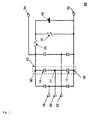
- FIG. 1 shows an exemplary first diode bridge with resistors and capacitance in a sketch 10, which corresponds to the prior art of a sum circuit.
- the diode bridge has three parallel bridge members 12, which are electrically guided with their first ends 26 to a first common output 32 and with their second ends 30 to a second common output 34th
- a bridge member 12 has two series-connected diodes 14, 16, with the electrical center 24, a respective input 18, 20, 22 of the diode bridge is connected, so that a total of three inputs result, as they are needed in a three-phase AC mains.
- a (charging) resistor 36 and a (discharge) resistor 38 are connected in series. Parallel to the (discharge) resistor 38, a capacitor 40 is connected.
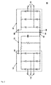
- FIG. 2 shows an exemplary inventive circuit arrangement 50.
- a first 52 and a second 60 diode bridge each with three bridge elements.
- the respective first DC side outputs 56 and 64 are electrically coupled to one another by a connection 68 and the second DC side outputs 58, 66 to a connection 70.
- the three inputs 54 of the first bridge 52 are intended to be connected to the inputs of a three-phase thyristor the three inputs of the second bridge 60 with the outputs of a three-phase Thyristorstellers.
- FIG. 3 shows an exemplary three-phase thyristor 84 according to the invention with voltage-limiting circuitry 82 in a schematic diagram 80.
- the three-phase thyristor 84 includes for each of its three phases a group 86, 88, 90 two counter-rotating thyristors 92, 94, to which a parallel connection of a resistor 96 and Capacitor 98 is provided.
- the three input and output side phases of thyristor controller 84 and circuit arrangement 82 are electrically combined at inputs 100 and outputs 102, respectively.
- an input-side supply network of, for example, 380V nominal voltage, through which the thyristor 84 is powered electrically via its inputs 100.
- the supply network can be assumed to be an ideal voltage source with a downstream network impedance.
- an output side load which is connected to the output 102 of the thyristor 84.
- a load can be broadly understood as an impedance. Both network impedance and load impedance have an influence on possible overvoltages, which are limited by the circuit arrangement 82 according to the invention.
- FIG. 4 shows in a representation 110 an exemplary single-phase thyristor with circuit arrangement and a neutral conductor 112, which is based on the basic principle of the three-phase thyristor with circuit arrangement FIG. 3 equivalent.
Landscapes
- Engineering & Computer Science (AREA)
- Power Engineering (AREA)
- Rectifiers (AREA)
Abstract
Die Erfindung betrifft eine Schaltungsanordnung für Thyristorsteller, umfassend ¢ eine erste Diodenbrücke 52 mit drei jeweils zwei Dioden umfassenden Brückengliedern, drei Eingängen 54 in der elektrischen Mitte der Brückenglieder sowie einem ersten 56 und einem zweiten 58 Ausgang, an dem die Enden der Brückenglieder miteinander verschaltet sind, ¢ wobei zwischen den beiden Ausgängen eine Reihenschaltung eines ersten und eines zweiten elektrischen Widerstandes vorgesehen ist, ¢ wobei parallel zu dem zweiten Widerstand eine elektrische Kapazität geschaltet ist. Die Erfindung betrifft auch einen Thyristorsteller mit erfindungsgemäßer Schaltungsanordnung.The invention relates to a circuit arrangement for a thyristor controller, comprising A first diode bridge 52 with three bridge members each comprising two diodes, three inputs 54 in the electrical center of the bridge members and a first 56 and a second 58 output, at which the ends of the bridge members are interconnected, € ¢ with a series connection of a first and a second electrical resistor being provided between the two outputs, € ¢ wherein an electrical capacitance is connected in parallel with the second resistor. The invention also relates to a thyristor controller with a circuit arrangement according to the invention.
Description
Die Erfindung betrifft eine Schaltungsanordnung für Thyristorsteller, umfassend eine erste Diodenbrücke mit drei jeweils zwei Dioden umfassenden Brückengliedern, drei Eingängen in der elektrischen Mitte der Brückenglieder sowie einen ersten und einen zweiten Ausgang, an dem die Enden der Brückenglieder miteinander verschaltet sind, wobei zwischen den beiden Ausgängen eine Reihenschaltung eines ersten und eines zweiten elektrischen Widerstandes vorgesehen ist und wobei parallel zu dem zweiten Widerstand eine elektrische Kapazität geschaltet ist.The invention relates to a circuit arrangement for thyristor, comprising a first diode bridge with three bridge elements each comprising two diodes, three inputs in the electrical center of the bridge members and a first and a second output at which the ends of the bridge members are interconnected, wherein between the two Outputs a series connection of a first and a second electrical resistance is provided and wherein an electrical capacitance is connected in parallel to the second resistor.
Es ist allgemein bekannt, dass Thyristoren dazu dienen können, die Leistungsaufnahme einer elektrischen Last zu steuern, indem der durch den Thyristor fließende Strom nur für einen jeweiligen Teil eines zur Verfügung stehenden Zeitintervalls aufrecht erhalten wird. Im Rahmen dieser Anmeldung sind insbesondere Lasten in Niederspannungsnetzen von beispielsweise dreiphasig 380V von Interesse, wobei selbstverständlich auch Spannungen im Bereich von 400V, 500V und auch 1200V von Relevanz sind. Ein Thyristor wird dann leitend, wenn nach dem Zünden genügend freie Ladungsträger zur Verfügung stehen, die einen Stromfluss gewährleisten. Er erlischt wieder, wenn die freien Ladungsträger zur Neige gehen bzw. nicht mehr vorhanden sind.It is well known that thyristors can serve to control the power consumption of an electrical load by maintaining the current flowing through the thyristor only for a respective portion of an available time interval. In the context of this application, loads in low-voltage networks of, for example, three-phase 380V are of particular interest, it being understood that voltages in the range of 400V, 500V and also 1200V are of relevance. A thyristor becomes conductive if, after ignition, sufficient free charge carriers are available to ensure a current flow. It goes out again when the free charge carriers are running out or are no longer available.
Wird eine induktive Last geschaltet, versucht diese Last den Strom aufrecht zu erhalten. Das führt dazu, dass sich nach erfolgter Abschaltung eine Spannung zwischen Anode und Kathode des Thyristors aufbaut, die diesen zerstören kann. Aus diesem Grund wird meist eine so genannte TSE (Träger Stau Effekt) - Beschaltung parallel zum Thyristor geschaltet. Üblicherweise besteht diese aus einem in Reihe geschalteten Widerstand R und einer Kapazität C. Diese RC-Beschaltung wird im Folgenden Einzelbeschaltung genannt.When an inductive load is switched, this load tries to maintain the current. The result is that after the shutdown voltage between Anode and cathode of the thyristor builds, which can destroy this. For this reason, usually a so-called TSE (carrier congestion effect) - wiring connected in parallel to the thyristor. Usually, this consists of a series resistor R and a capacitor C. This RC circuit is called Einzelbeschaltung in the following.
Die Auslegekriterien für die Einzelbeschaltung sind unter Anderem:
- die maximale Sperrspannung des Thyristors,
- die zulässige Spannungssteilheit am Thyristor,
- der zulässige Strom beim Einschalten des Thyristors,
- Verluste in der Beschaltung sowie im Thyristor.
- the maximum blocking voltage of the thyristor,
- the permissible voltage gradient at the thyristor,
- the permissible current when switching on the thyristor,
- Losses in the wiring and in the thyristor.
Hinweise für die Auslegung von DC-Mittelpunktschaltungen und -brücken erhält man üblicherweise aus diverser Literatur sowie von den Thyristorproduzenten. Wichtig ist in diesem Zusammenhang, dass die Beschaltungsverluste weitestgehend von der Größe der Beschaltungskapazität abhängen.Guidelines for the design of DC midpoint circuits and bridges are usually obtained from various literature as well as from thyristor producers. It is important in this context that the wiring losses depend largely on the size of the Beschaltungsungskapazität.
Beim Einschalten des Thyristors entsteht in der Beschaltung durch die Kapazität ein Energieverlust in Höhe von ½ * C * U2 und beim Ausschalten ein meist noch höherer Wert, weil die Spannung am Thyristor überschwingt.When the thyristor is switched on, the capacitance causes an energy loss in the circuit of ½ * C * U 2 and, when switched off, a value that is usually even higher because the voltage at the thyristor overshoots.
Zur Verlustreduktion ist die Beschaltungskapazität möglichst klein zu machen, im Idealfall so klein, dass die Einzelbeschaltung nur noch für die Begrenzung der Spannungssteilheit zuständig ist. Dies führt allerdings zu einem großen Überschwingen der Spannung am Thyristor. Eine Abhilfemaßnahme bietet bei diversen Schaltungsvarianten (zum Beispiel Mittelpunkt- oder Brückenschaltungen) eine sogenannte Summenbeschaltung, umfassend beispielsweise 6 Dioden in B6-Konfiguration, einen Auf- und Entladewiderstand sowie eine Kapazität.In order to reduce the loss, the circuit capacitance must be made as small as possible, ideally so small that the individual circuit is only responsible for limiting the voltage gradient. However, this leads to a large overshoot of the voltage at the thyristor. A remedy for various circuit variants (for example center or bridge circuits) comprises a so-called summation circuit comprising, for example, 6 diodes in B6 configuration, charging and discharging resistance and a capacity.
Bei einer Summenbeschaltung wird die Kapazität bei einer B6-Brücke beim Einschalten auf den Spitzenwert der verketteten Spannung aufgeladen. Ist der Schwingkreis bestehend aus Netzinduktivität und Summenbeschaltungskapazität zu schwach gedämpft, wird die Kapazität sogar überladen.In a summation circuit, the capacitance on a B6 bridge is charged at power-up to the peak of the chained voltage. If the resonant circuit consisting of the mains inductance and the sum-circuit capacitance is too weakly damped, the capacitance will even become overloaded.
Der Entladewiderstand sorgt dafür, dass die Beschaltungskapazität dauernd entladen wird, so dass sie im Betrieb die in der Induktivität gespeicherte Energie zyklisch aufnehmen kann. Die Beschaltungskapazität der Summenbeschaltung "klemmt" die Spannung auf einen Wert, bei dem sich das Gleichgewicht einstellt, weil diese größer ist als die Kapazitäten der Einzelbeschaltung. Die sich hierbei ergebenden Verluste sind im Vergleich zu einer entsprechenden Einzelbeschaltung deutlich reduziert.The discharge resistor ensures that the circuit capacitance is constantly discharged, so that during operation it can record the energy stored in the inductance cyclically. The circuit capacitance of the summation circuit "clamps" the voltage to a value at which the equilibrium sets because it is greater than the capacities of the individual circuit. The resulting losses are significantly reduced compared to a corresponding individual circuit.
Für Thyristorsteller gibt es nur eine deutlich kleinere Auswahl an Beschaltungen als für DC-Regler. Das hängt unter anderem damit zusammen, dass es keine polarisierten Beschaltungen gibt. Die typische Beschaltung ist ein RC-Glied, in mancher Literatur finden sich zusätzlich MOVs (Metal Oxide Varistor) als Beschaltungvariante parallel zum Thyristor.There are only a considerably smaller selection of circuits for thyristor controllers than for DC controllers. This is partly due to the fact that there are no polarized circuits. The typical wiring is an RC element, in some literature there are additional MOVs (Metal Oxide Varistor) as a wiring variant parallel to the thyristor.
MOVs als Beschaltung sind jedoch nur sehr bedingt geeignet. Dies hat unter anderem den Hintergrund, dass idealerweise eine rechtwinkelige Kennlinie gewünscht ist, bei welcher sofort nach Eintreten der Spannungsüberhöhung ein entsprechender Stromfluss eintritt, durch den die Spannungserhöhung begrenzt wird. Dies ist bei Varistoren nicht der Fall, weil die U/I-Kennlinie keinen ausgeprägten Knick aufweist, sondern eher träge ist. Ein anderer Nachteil von Varistoren ist das schnelle Altern bei permanenter Beanspruchung.MOVs as wiring are only very suitable. This has, inter alia, the background that ideally a rectangular characteristic curve is desired, in which immediately after the onset of voltage increase, a corresponding current flow occurs, by means of which the voltage increase is limited. This is not the case with varistors because the U / I characteristic does not have a pronounced kink, but rather is sluggish. Another disadvantage of varistors is fast aging under permanent load.
Nachteilig an dem Stand der Technik ist, dass sich bei einem Thyristorsteller zwar die gleiche Summenbeschaltung einbauen lässt wie bei einer B6-Thyristorbrücke, diese aber nur sehr bedingt wirkt. Grund dafür ist, dass die Summenbeschaltung bei einer B6 Thyristorbrücke "zwischen den Phasen" wirkt, also quasi parallel zu einer Reihenschaltung von jeweils zwei Thyristoren wirkt und so die Spannungsspitzen am Thyristor kappt. Beim Thyristorsteller muss die Beschaltung aber nicht nur zwischen den Phasen, sondern auch zwischen Eingang und Ausgang des Thyristorstellers wirken.A disadvantage of the prior art is that in a thyristor while the same sum circuit can be installed as in a B6 thyristor, but this has only very limited. The reason for this is that the summation circuit acts "between the phases" in the case of a B6 thyristor bridge, that is to say acts in parallel with a series connection of two thyristors and thus cuts off the voltage peaks at the thyristor. With the thyristor controller, however, the circuitry does not only have to act between the phases, but also between the input and the output of the thyristor controller.
Ausgehend von diesem Stand der Technik ist es Aufgabe der Erfindung, eine verbesserte Schaltungsanordnung für Thyristorsteller anzugeben, durch welche Überspannungen in zuverlässiger Weise begrenzt werden. Aufgabe der Erfindung ist es auch, einen entsprechenden Thyristorsteller anzugeben.Based on this prior art, it is an object of the invention to provide an improved circuit arrangement for thyristor, by which surges are limited in a reliable manner. The object of the invention is also to provide a corresponding thyristor.
Diese Aufgabe wird gelöst durch eine Schaltungsanordnung der eingangs genannten Art. Diese ist gekennzeichnet durch
- eine zweite Diodenbrücke mit drei jeweils zwei Dioden umfassenden Brückengliedern, drei Eingängen in der elektrischen Mitte der Brückenglieder sowie einem ersten und einem zweiten Ausgang, an dem die Enden der Brückenglieder miteinander verschaltet sind,
- wobei die ersten und zweiten Ausgänge der Diodenbrücken jeweils mit identischer Polarität elektrisch miteinander verbunden sind,
- wobei die Schaltungsanordnung dafür vorgesehen ist, dass die drei Eingänge der ersten Brücke mit den Eingängen eines dreiphasigen Thyristorstellers verbunden werden und dass die drei Eingänge der zweiten Brücke mit dessen Ausgängen verbunden werden.
- a second diode bridge having three bridge elements each comprising two diodes, three inputs in the electrical center of the bridge elements and a first and a second output at which the ends of the bridge elements are interconnected,
- wherein the first and second outputs of the diode bridges are each electrically connected to each other with identical polarity,
- wherein the circuit arrangement is arranged so that the three inputs of the first bridge are connected to the inputs of a three-phase thyristor and that the three inputs of the second bridge are connected to its outputs.
Die Grundidee der Erfindung besteht darin, ausgehend von der bekannten Summenbeschaltung eine weitere Diodenbrücke zu installieren, deren drei Eingänge beziehungsweise wechselspannungsseitige Anschlüsse mit den drei Ausgängen des Thyristorstellers verbunden sind. Die gleichspannungsseitigen Ausgänge der Diodenbrücken sind hierbei ebenfalls miteinander verbunden.The basic idea of the invention is to install, starting from the known summation circuit, a further diode bridge whose three inputs or AC-side connections are connected to the three outputs of the thyristor controller. The DC voltage side outputs of the diode bridges are in this case also connected to each other.
Beim Einschalten des Stellers an das Netz verhält sich die erfindungsgemäße Schaltungsanordnung wie die Summenbeschaltung einer Mittelpunkt- oder einer Brückenschaltung. Die Kapazität wird auf den Spitzenwert der verketteten Spannung aufgeladen.When the actuator is switched on to the network, the circuit arrangement according to the invention behaves like the sum circuit of a mid-point or a bridge circuit. The capacity is charged to the peak value of the chained voltage.
Die Thyristoren selbst liegen aber nicht wie bei der Brückenschaltung zwischen den Phasen, sondern sie liegen in den Außenleitern. Sie sind durch die jeweilige Last im Netz von den andern Thyristoren getrennt. Eine Kommutierung, bei der nur die Netzinduktivität strombegrenzend wirkt, gibt es beim Thyristorsteller nicht. Vielmehr sind Netzinduktivität, Thyristorsteller und Last in Reihe geschaltet.The thyristors themselves are not located between the phases as in the bridge circuit, but they are located in the outer conductors. They are separated from the other thyristors by the respective load in the network. A commutation in which only the network inductance has a current-limiting effect does not exist with the thyristor controller. Rather, mains inductance, thyristor and load are connected in series.
An den Thyristoren selbst liegt nicht die verkettete Spannung sondern die Strangspannung an. Diese ist um √3 kleiner als die verkettete Spannung. Erst wenn eine Spannung höher wird als die Spannung an der Kapazität beginnt ein Strom über die entsprechenden Dioden und die Kapazität zu fließen und schneidet damit die Spannungsspitzen ab.The thyristors themselves are not the chained voltage but the strand voltage. This is smaller by √3 than the chained voltage. Only when a voltage is higher than the voltage at the capacity starts a current over the corresponding diodes and the capacity to flow, thus cutting off the voltage spikes.
Für die Auslegung des Entladewiderstandes gelten die oben genannten Randbedingungen. Die Schaltungsanordnung schneidet erst dann die Spannungsspitzen ab, wenn die verkettete Spannung überschritten wird.For the design of the discharge resistance, the above-mentioned boundary conditions apply. The circuit arrangement only cuts off the voltage peaks when the chained voltage is exceeded.
Es ergeben sich insbesondere folgende Vorteile der erfindungsgemäßen Schaltungsanordnung:
- Die Schaltungsanordnung ist ausschließlich aus passiven Komponenten aufgebaut und damit sehr robust.
- Spannungsspitzen werden sehr exakt abgeschnitten, abhängig nur von der Netzspannung und dem Lade- und Entladewiderstand. In weiten Bereichen ist das Verhalten fast ausschließlich von der Netzspannung abhängig. Wird die Netzspannung kleiner, greift auch die obige Beschaltung entsprechend früher ein.
- Auch bei Blocktaktung, wenn die Thyristoren längere Zeit Strom führen, wird die Kapazität nicht entladen. Die elektrischen Komponenten werden dadurch nicht mit extremen Stoßströmen beansprucht.
- Toleranzen, wie z.B. bei Varistoren, spielen keine Rolle, die Schaltung stellt sich automatisch auf die Netzspannung ein.
- Die Schaltungsanordnung wirkt sowohl bei internen als auch bei extern erzeugten Überspannungen.
- The circuit arrangement is constructed exclusively of passive components and thus very robust.
- Voltage peaks are cut off very precisely, depending only on the mains voltage and the charging and discharging resistance. In many areas, the behavior almost exclusively depends on the mains voltage. If the mains voltage is lower, the above wiring will intervene earlier.
- Even with block timing, when the thyristors run power for a long time, the capacity is not discharged. The electrical components are thus not subjected to extreme surge currents.
- Tolerances, such as with varistors, are irrelevant, the circuit adjusts itself automatically to the mains voltage.
- The circuit arrangement acts both in internal and externally generated overvoltages.
Die erfindungsgemäße Aufgabe wird auch gelöst durch einen Thyristorsteller mit drei Eingängen und drei Ausgängen und einer erfindungsgemäßen Schaltungsanordnung, wobei die die drei Eingänge der ersten Brücke der Schaltungsanordnung mit den Eingängen des dreiphasigen Thyristorstellers verbunden sind und die drei Eingänge der zweiten Brücke mit dessen Ausgängen. Die sich ergebenden Vorteile wurden bereits im Rahmen der erfindungsgemäßen Schaltungsauslegung erläutert.The object of the invention is also achieved by a thyristor with three inputs and three outputs and a circuit arrangement according to the invention, wherein the three inputs of the first bridge of the circuit arrangement are connected to the inputs of the three-phase thyristor and the three inputs of the second bridge with its outputs. The resulting advantages have already been explained in the context of the circuit design according to the invention.
Gemäß einer bevorzugten Variante der erfindungsgemäßen Schaltungsanordnung umfasst wenigstens eine der Diodenbrücken ein viertes Brückenglied, welches dafür vorgesehen ist, in seiner elektrischen Mitte mit einem Neutralleiter N verbunden zu werden. Somit ist in vorteilhafter Weise auch ein einphasiger Betrieb ermöglicht.According to a preferred variant of the circuit arrangement according to the invention, at least one of the diode bridges comprises a fourth bridge member which is therefor is provided to be connected in its electrical center with a neutral conductor N. Thus, a single-phase operation is possible in an advantageous manner.
Gemäß einer bevorzugten Variante des erfindungsgemäßen Thyristorstellers sind zwischen dem Eingang und dem Ausgang einer jeweiligen Phase des Thyristorstellers zwei gegenläufig verschaltete Thyristoren mit einer Einzelbeschaltung aus einem in Reihe geschaltetem Widerstand und einer Kapazität vorhanden. Dies ist eine geeignete Grundschaltung zum biploaren Durchschalten beziehungsweise Sperren einer Phase. Vorzugsweise sind die Kapazitäten der Einzelbeschaltung der Thyristoren kleiner als die Kapazität der Schaltungsanordnung.According to a preferred variant of the thyristor according to the invention, two oppositely connected thyristors with a single circuit of a series-connected resistor and a capacitor are present between the input and the output of a respective phase of the thyristor. This is a suitable basic circuit for bipolar switching or blocking of a phase. Preferably, the capacitances of the individual circuit of the thyristors are smaller than the capacitance of the circuit arrangement.
Die erfindungsgemäße Aufgabe wird auch gelöst durch eine Schaltungsanordnung für Thyristorsteller, umfassend
- eine erste Diodenbrücke mit zwei jeweils zwei Dioden umfassenden Brückengliedern, zwei Eingängen in der elektrischen Mitte der Brückenglieder sowie einem ersten und einem zweiten Ausgang, an dem die Enden der Brückenglieder miteinander verschaltet sind,
- wobei zwischen den beiden Ausgängen eine Reihenschaltung eines ersten und eines zweiten elektrischen Widerstandes vorgesehen ist,
- wobei parallel zu dem zweiten Widerstand eine elektrische Kapazität geschaltet ist,
gekennzeichnet durch - eine zweite Diodenbrücke mit einem jeweils zwei Dioden umfassenden Brückenglied, einem Eingang in der elektrischen Mitte des Brückengliedes, sowie einem ersten und einem zweiten Ausgang, mit denen die jeweiligen Enden des Brückengliedes verschaltet sind,
- wobei die ersten und zweiten Ausgänge der Diodenbrücken jeweils mit identischer Polarität elektrisch miteinander verbunden sind,
- wobei die Schaltungsanordnung dafür vorgesehen ist, dass der erste Eingang der ersten Brücke mit dem Eingang eines einphasigen Thyristorstellers verbunden wird, dass der Eingang der zweiten Brücke mit dessen Ausgang verbunden wird und dass der zweite Eingang der ersten Brücke dafür vorgesehen ist, mit einem Neutralleiter N verbunden zu werden.
- a first diode bridge having two bridge elements each comprising two diodes, two inputs in the electrical center of the bridge elements and a first and a second output at which the ends of the bridge elements are interconnected,
- wherein a series circuit of a first and a second electrical resistance is provided between the two outputs,
- wherein an electrical capacitance is connected in parallel to the second resistor,
marked by - a second diode bridge having a bridge element each comprising two diodes, an input in the electrical center of the bridge element, and a first and a second output, with which the respective ends of the bridge element are connected,
- wherein the first and second outputs of the diode bridges are each electrically connected to each other with identical polarity,
- wherein the circuit arrangement is provided so that the first input of the first bridge is connected to the input of a single-phase thyristor, that the input of the second bridge is connected to the output thereof and that the second input of the first bridge is provided with a neutral conductor N. to be connected.
Diese Ausführungsform entspricht der einphasigen Form der zuvor offenbarten dreiphasigen Variante, wobei hier eine Verbindung zu einem Neutralleiter obligatorisch für den Betrieb ist. Die sich ergebenden Vorteile entsprechen im Wesentlichen den zuvor erörterten Vorteilen der dreiphasigen Variante. Selbstverständlich sind auch dreiphasige Varianten mit beispielsweise zwei B12 Diodenbrücken denkbar.This embodiment corresponds to the single-phase form of the previously disclosed three-phase variant, in which case a connection to a neutral conductor is obligatory for the operation. The resulting benefits are essentially the same as the previously discussed advantages of the three-phase variant. Of course, three-phase variants with, for example, two B12 diode bridges are also conceivable.
Weitere vorteilhafte Ausgestaltungsmöglichkeiten sind den weiteren abhängigen Ansprüchen zu entnehmen.Further advantageous embodiment possibilities can be found in the further dependent claims.
Anhand der in den Zeichnungen dargestellten Ausführungsbeispiele sollen die Erfindung, weitere Ausführungsformen und weitere Vorteile näher beschrieben werden.Reference to the embodiments illustrated in the drawings, the invention, further embodiments and other advantages will be described in detail.
Es zeigen:
- Fig. 1
- eine exemplarische erste Diodenbrücke mit Widerstand und Kapazität,
- Fig. 2
- eine exemplarische Schaltungsanordnung,
- Fig. 3
- einen exemplarischen Thyristorsteller mit Schaltungsanordnung sowie
- Fig. 4
- einen exemplarischen dreiphasigen Thyristorsteller mit Schaltungsanordnung.
- Fig. 1
- an exemplary first diode bridge with resistance and capacitance,
- Fig. 2
- an exemplary circuit arrangement,
- Fig. 3
- an exemplary thyristor with circuit arrangement as well
- Fig. 4
- an exemplary three-phase thyristor with circuit arrangement.
Ein Brückenglied 12 weist zwei in Reihe geschaltete Dioden 14, 16 auf, mit deren elektrischer Mitte 24 ein jeweiliger Eingang 18, 20, 22 der Diodenbrücke verbunden ist, so dass sich insgesamt drei Eingänge ergeben, wie sie bei einem dreiphasigen Wechselspannungsnetz benötigt werden.A
Zwischen den beiden gleichspannungsseitigen Ausgängen 32, 34 sind ein (Lade-) Widerstand 36 sowie ein (Entlade-) Widerstand 38 in Reihe geschaltet. Parallel zum (Entlade-) Widerstand 38 ist eine Kapazität 40 geschaltet. Eine typische Wertekombination für die genannten Komponenten ist beispielsweise 1Ω für den Ladewiderstand 50 kΩ für den Entladewiderstand 38 und 6,8µF für die Kapazität 40 bei einer Nennspannung von beispielsweise 380V.Between the two DC voltage side outputs 32, 34, a (charging)
Die jeweils drei ein- und ausgangsseitigen Phasen von Thyristorsteller 84 und Schaltungsanordnung 82 sind an Eingängen 100 beziehungsweise Ausgängen 102 jeweils elektrisch zusammengefasst.The three input and output side phases of
Nicht gezeigt ist ein eingangsseitiges Versorgungsnetz von beispielsweise 380V Nennspannung, durch welches der Thyristorsteller 84 über seine Eingänge 100 elektrisch versorgt wird. Das Versorgungsnetz kann vereinfacht als ideale Spannungsquelle mit einer nachgeschalteten Netzimpedanz angenommen werden. Ebenfalls nicht gezeigt ist eine ausgangsseitige Last, welche an den Ausgang 102 des Thyristorstellers 84 angeschlossen ist. Eine Last kann im weiteren Sinne als eine Impedanz angenommen werden. Sowohl Netzimpedanz als auch Lastimpedanz haben einen Einfluss auf eventuell entstehende Überspannungen, welche durch die erfindungsgemäße Schaltungsanordnung 82 begrenzt werden.Not shown is an input-side supply network of, for example, 380V nominal voltage, through which the
- 1010
- exemplarische erste Diodenbrücke mit Widerstand und Kapazitätexemplary first diode bridge with resistance and capacitance
- 1212
- Brückengliedbridge member
- 1414
- erste Diode von Brückengliedfirst diode of bridge member
- 1616
- zweite Diode von Brückengliedsecond diode of bridge member
- 1818
- erster Eingang von erster Diodenbrückefirst input of first diode bridge
- 2020
- zweiter Eingang von erster Diodenbrückesecond input of first diode bridge
- 2222
- dritter Eingang von erster Diodenbrückethird input from first diode bridge
- 2424
- elektrische Mitte von Brückengliedelectrical center of bridge link
- 2626
- erstes Ende von Brückengliedfirst end of bridge member
- 3030
- zweites Ende von Brückengliedsecond end of bridge member
- 3232
- erster Ausgang von erster Diodenbrückefirst output of first diode bridge
- 3434
- zweiter Ausgang von erster Diodenbrückesecond output from first diode bridge
- 3636
- erster Widerstandfirst resistance
- 3838
- zweiter Widerstandsecond resistance
- 4040
- Kapazitätcapacity
- 5050
- exemplarische Schaltungsanordnungexemplary circuit arrangement
- 5252
- erste Diodenbrückefirst diode bridge
- 5454
- Eingänge von erster DiodenbrückeInputs of first diode bridge
- 5656
- erster Ausgang von erster Diodenbrückefirst output of first diode bridge
- 5858
- zweiter Ausgang von erster Diodenbrückesecond output from first diode bridge
- 6060
- zweite Diodenbrückesecond diode bridge
- 6262
- Eingänge von zweiter DiodenbrückeInputs from second diode bridge
- 6464
- erster Ausgang von zweiter Diodenbrückefirst output from second diode bridge
- 6666
- zweiter Ausgang von zweiter Diodenbrückesecond output from second diode bridge
- 6868
- Verbindung von ersten AusgängenConnection of first outputs
- 7070
- Verbindung von zweiten AusgängenConnection of second outputs
- 8080
- exemplarischer Thyristorsteller mit Schaltungsanordnungexemplary thyristor with circuit arrangement
- 8282
- exemplarische Schaltungsanordnungexemplary circuit arrangement
- 8484
- dreiphasiger Thyristorstellerthree-phase thyristor controller
- 8686
- Thyristorsteller für erste PhaseThyristor controller for first phase
- 8888
- Thyristorsteller für zweite PhaseThyristor controller for second phase
- 9090
- Thyristorsteller für dritte PhaseThyristor controller for third phase
- 9292
- erster Thyristorfirst thyristor
- 9494
- zweiter Thyristorsecond thyristor
- 9696
- Widerstandresistance
- 9898
- Kapazitätcapacity
- 100100
- Eingänge von dreiphasigem ThyristorstellerInputs of three-phase thyristor controller
- 102102
- Ausgänge von dreiphasigem ThyristorstellerOutputs of three-phase thyristor controller
- 110110
- exemplarischer einphasiger Thyristorsteller mit SchaltungsanordnungExemplary single-phase thyristor with circuit arrangement
- 112112
- Neutralleiterneutral
Claims (5)
gekennzeichnet durch
marked by
gekennzeichnet durch
marked by
Priority Applications (1)
| Application Number | Priority Date | Filing Date | Title |
|---|---|---|---|
| EP15150286.1A EP3043473B1 (en) | 2015-01-07 | 2015-01-07 | Circuit assembly for thyristor controller |
Applications Claiming Priority (1)
| Application Number | Priority Date | Filing Date | Title |
|---|---|---|---|
| EP15150286.1A EP3043473B1 (en) | 2015-01-07 | 2015-01-07 | Circuit assembly for thyristor controller |
Publications (2)
| Publication Number | Publication Date |
|---|---|
| EP3043473A1 true EP3043473A1 (en) | 2016-07-13 |
| EP3043473B1 EP3043473B1 (en) | 2022-05-18 |
Family
ID=52232096
Family Applications (1)
| Application Number | Title | Priority Date | Filing Date |
|---|---|---|---|
| EP15150286.1A Active EP3043473B1 (en) | 2015-01-07 | 2015-01-07 | Circuit assembly for thyristor controller |
Country Status (1)
| Country | Link |
|---|---|
| EP (1) | EP3043473B1 (en) |
Citations (7)
| Publication number | Priority date | Publication date | Assignee | Title |
|---|---|---|---|---|
| DE1538154A1 (en) * | 1966-03-29 | 1969-07-31 | Siemens Ag | Converter arrangement with thyristors |
| DE8716005U1 (en) * | 1987-12-03 | 1988-02-11 | Siemens AG, 1000 Berlin und 8000 München | Terminal connection module |
| DE19844823C1 (en) * | 1998-09-30 | 1999-10-28 | Siemens Ag | Thyristor circuit for high power static converter |
| US20010026427A1 (en) * | 2000-02-08 | 2001-10-04 | Siemens Ag. | Overvoltage protection apparatus for a matrix converter |
| DE10221714A1 (en) * | 2002-05-16 | 2003-11-27 | Abb Patent Gmbh | Overvoltage protection arrangement for direct and alternating voltage networks, has capacitor additionally connected after varistor in series circuit with break-over diode element |
| US20060220471A1 (en) * | 2005-03-31 | 2006-10-05 | Reinhard Joho | Generator switch |
| CN101917011A (en) * | 2010-09-06 | 2010-12-15 | 东南大学 | Power quality comprehensive control method and device for electric railway traction power supply system |
-
2015
- 2015-01-07 EP EP15150286.1A patent/EP3043473B1/en active Active
Patent Citations (7)
| Publication number | Priority date | Publication date | Assignee | Title |
|---|---|---|---|---|
| DE1538154A1 (en) * | 1966-03-29 | 1969-07-31 | Siemens Ag | Converter arrangement with thyristors |
| DE8716005U1 (en) * | 1987-12-03 | 1988-02-11 | Siemens AG, 1000 Berlin und 8000 München | Terminal connection module |
| DE19844823C1 (en) * | 1998-09-30 | 1999-10-28 | Siemens Ag | Thyristor circuit for high power static converter |
| US20010026427A1 (en) * | 2000-02-08 | 2001-10-04 | Siemens Ag. | Overvoltage protection apparatus for a matrix converter |
| DE10221714A1 (en) * | 2002-05-16 | 2003-11-27 | Abb Patent Gmbh | Overvoltage protection arrangement for direct and alternating voltage networks, has capacitor additionally connected after varistor in series circuit with break-over diode element |
| US20060220471A1 (en) * | 2005-03-31 | 2006-10-05 | Reinhard Joho | Generator switch |
| CN101917011A (en) * | 2010-09-06 | 2010-12-15 | 东南大学 | Power quality comprehensive control method and device for electric railway traction power supply system |
Also Published As
| Publication number | Publication date |
|---|---|
| EP3043473B1 (en) | 2022-05-18 |
Similar Documents
| Publication | Publication Date | Title |
|---|---|---|
| EP3895313B1 (en) | Switching device for separating a current path | |
| EP3853957B1 (en) | Electronic switch with overvoltage protection | |
| EP3583670A2 (en) | Electronic circuit-breaker for a load that can be connected to a low voltage dc-voltage network | |
| DE112016000220T5 (en) | POWER CONVERSION EQUIPMENT | |
| EP3367567A1 (en) | Switching device for separating a current path | |
| EP3794730B1 (en) | Switching device for separating a current path | |
| EP3571750B1 (en) | Apparatus for limiting voltage for a dc voltage network | |
| DE2634667A1 (en) | PERFORMANCE CONTROLLER | |
| DE102018215881B3 (en) | Device and method for coupling two direct current networks | |
| EP4064563B1 (en) | Electronic switch | |
| DE102013219173A1 (en) | Power supply for electrical focusing of electron beams | |
| EP2845214B1 (en) | Apparatus for switching in a dc voltage mains | |
| EP2599213B1 (en) | Converter system and method for operating such a converter system | |
| EP3361596B1 (en) | Battery with a battery management system which comprises an electronic switching circuit | |
| EP3895312B1 (en) | Electronic switch with power regulation | |
| DE102019107112B3 (en) | Switching device, voltage supply system, method for operating a switching device and manufacturing method | |
| EP3236572A1 (en) | Power electronic switching cell and converter circuit with such switching cells | |
| EP1817828B1 (en) | Additional device in a current limiter for limiting current in the event of a fault | |
| EP3043473B1 (en) | Circuit assembly for thyristor controller | |
| EP3391524B1 (en) | Convertermodule for multilevelconverters and its workingprocess | |
| DE102014212263A1 (en) | Circuit arrangement for self-regulating starting current limitation of an electrical machine | |
| DE102017106770B4 (en) | Circuit arrangement for protection against network overvoltages for power converters in vehicles, in particular in vehicles connected to overhead lines | |
| EP3736932A1 (en) | Dc network | |
| EP1619783B1 (en) | Converter with limited voltage rise | |
| DE60013109T2 (en) | Static circuit breaker |
Legal Events
| Date | Code | Title | Description |
|---|---|---|---|
| PUAI | Public reference made under article 153(3) epc to a published international application that has entered the european phase |
Free format text: ORIGINAL CODE: 0009012 |
|
| AK | Designated contracting states |
Kind code of ref document: A1 Designated state(s): AL AT BE BG CH CY CZ DE DK EE ES FI FR GB GR HR HU IE IS IT LI LT LU LV MC MK MT NL NO PL PT RO RS SE SI SK SM TR |
|
| AX | Request for extension of the european patent |
Extension state: BA ME |
|
| STAA | Information on the status of an ep patent application or granted ep patent |
Free format text: STATUS: REQUEST FOR EXAMINATION WAS MADE |
|
| 17P | Request for examination filed |
Effective date: 20170113 |
|
| STAA | Information on the status of an ep patent application or granted ep patent |
Free format text: STATUS: EXAMINATION IS IN PROGRESS |
|
| 17Q | First examination report despatched |
Effective date: 20200102 |
|
| GRAP | Despatch of communication of intention to grant a patent |
Free format text: ORIGINAL CODE: EPIDOSNIGR1 |
|
| STAA | Information on the status of an ep patent application or granted ep patent |
Free format text: STATUS: GRANT OF PATENT IS INTENDED |
|
| INTG | Intention to grant announced |
Effective date: 20211210 |
|
| GRAS | Grant fee paid |
Free format text: ORIGINAL CODE: EPIDOSNIGR3 |
|
| GRAA | (expected) grant |
Free format text: ORIGINAL CODE: 0009210 |
|
| STAA | Information on the status of an ep patent application or granted ep patent |
Free format text: STATUS: THE PATENT HAS BEEN GRANTED |
|
| AK | Designated contracting states |
Kind code of ref document: B1 Designated state(s): AL AT BE BG CH CY CZ DE DK EE ES FI FR GB GR HR HU IE IS IT LI LT LU LV MC MK MT NL NO PL PT RO RS SE SI SK SM TR |
|
| REG | Reference to a national code |
Ref country code: GB Ref legal event code: FG4D Free format text: NOT ENGLISH |
|
| REG | Reference to a national code |
Ref country code: CH Ref legal event code: EP |
|
| REG | Reference to a national code |
Ref country code: IE Ref legal event code: FG4D Free format text: LANGUAGE OF EP DOCUMENT: GERMAN |
|
| REG | Reference to a national code |
Ref country code: DE Ref legal event code: R096 Ref document number: 502015015843 Country of ref document: DE |
|
| REG | Reference to a national code |
Ref country code: AT Ref legal event code: REF Ref document number: 1493724 Country of ref document: AT Kind code of ref document: T Effective date: 20220615 |
|
| REG | Reference to a national code |
Ref country code: LT Ref legal event code: MG9D |
|
| REG | Reference to a national code |
Ref country code: NL Ref legal event code: MP Effective date: 20220518 |
|
| PG25 | Lapsed in a contracting state [announced via postgrant information from national office to epo] |
Ref country code: SE Free format text: LAPSE BECAUSE OF FAILURE TO SUBMIT A TRANSLATION OF THE DESCRIPTION OR TO PAY THE FEE WITHIN THE PRESCRIBED TIME-LIMIT Effective date: 20220518 Ref country code: PT Free format text: LAPSE BECAUSE OF FAILURE TO SUBMIT A TRANSLATION OF THE DESCRIPTION OR TO PAY THE FEE WITHIN THE PRESCRIBED TIME-LIMIT Effective date: 20220919 Ref country code: NO Free format text: LAPSE BECAUSE OF FAILURE TO SUBMIT A TRANSLATION OF THE DESCRIPTION OR TO PAY THE FEE WITHIN THE PRESCRIBED TIME-LIMIT Effective date: 20220818 Ref country code: NL Free format text: LAPSE BECAUSE OF FAILURE TO SUBMIT A TRANSLATION OF THE DESCRIPTION OR TO PAY THE FEE WITHIN THE PRESCRIBED TIME-LIMIT Effective date: 20220518 Ref country code: LT Free format text: LAPSE BECAUSE OF FAILURE TO SUBMIT A TRANSLATION OF THE DESCRIPTION OR TO PAY THE FEE WITHIN THE PRESCRIBED TIME-LIMIT Effective date: 20220518 Ref country code: HR Free format text: LAPSE BECAUSE OF FAILURE TO SUBMIT A TRANSLATION OF THE DESCRIPTION OR TO PAY THE FEE WITHIN THE PRESCRIBED TIME-LIMIT Effective date: 20220518 Ref country code: GR Free format text: LAPSE BECAUSE OF FAILURE TO SUBMIT A TRANSLATION OF THE DESCRIPTION OR TO PAY THE FEE WITHIN THE PRESCRIBED TIME-LIMIT Effective date: 20220819 Ref country code: FI Free format text: LAPSE BECAUSE OF FAILURE TO SUBMIT A TRANSLATION OF THE DESCRIPTION OR TO PAY THE FEE WITHIN THE PRESCRIBED TIME-LIMIT Effective date: 20220518 Ref country code: ES Free format text: LAPSE BECAUSE OF FAILURE TO SUBMIT A TRANSLATION OF THE DESCRIPTION OR TO PAY THE FEE WITHIN THE PRESCRIBED TIME-LIMIT Effective date: 20220518 Ref country code: BG Free format text: LAPSE BECAUSE OF FAILURE TO SUBMIT A TRANSLATION OF THE DESCRIPTION OR TO PAY THE FEE WITHIN THE PRESCRIBED TIME-LIMIT Effective date: 20220818 |
|
| PG25 | Lapsed in a contracting state [announced via postgrant information from national office to epo] |
Ref country code: RS Free format text: LAPSE BECAUSE OF FAILURE TO SUBMIT A TRANSLATION OF THE DESCRIPTION OR TO PAY THE FEE WITHIN THE PRESCRIBED TIME-LIMIT Effective date: 20220518 Ref country code: PL Free format text: LAPSE BECAUSE OF FAILURE TO SUBMIT A TRANSLATION OF THE DESCRIPTION OR TO PAY THE FEE WITHIN THE PRESCRIBED TIME-LIMIT Effective date: 20220518 Ref country code: LV Free format text: LAPSE BECAUSE OF FAILURE TO SUBMIT A TRANSLATION OF THE DESCRIPTION OR TO PAY THE FEE WITHIN THE PRESCRIBED TIME-LIMIT Effective date: 20220518 Ref country code: IS Free format text: LAPSE BECAUSE OF FAILURE TO SUBMIT A TRANSLATION OF THE DESCRIPTION OR TO PAY THE FEE WITHIN THE PRESCRIBED TIME-LIMIT Effective date: 20220918 |
|
| PG25 | Lapsed in a contracting state [announced via postgrant information from national office to epo] |
Ref country code: SM Free format text: LAPSE BECAUSE OF FAILURE TO SUBMIT A TRANSLATION OF THE DESCRIPTION OR TO PAY THE FEE WITHIN THE PRESCRIBED TIME-LIMIT Effective date: 20220518 Ref country code: SK Free format text: LAPSE BECAUSE OF FAILURE TO SUBMIT A TRANSLATION OF THE DESCRIPTION OR TO PAY THE FEE WITHIN THE PRESCRIBED TIME-LIMIT Effective date: 20220518 Ref country code: RO Free format text: LAPSE BECAUSE OF FAILURE TO SUBMIT A TRANSLATION OF THE DESCRIPTION OR TO PAY THE FEE WITHIN THE PRESCRIBED TIME-LIMIT Effective date: 20220518 Ref country code: EE Free format text: LAPSE BECAUSE OF FAILURE TO SUBMIT A TRANSLATION OF THE DESCRIPTION OR TO PAY THE FEE WITHIN THE PRESCRIBED TIME-LIMIT Effective date: 20220518 Ref country code: DK Free format text: LAPSE BECAUSE OF FAILURE TO SUBMIT A TRANSLATION OF THE DESCRIPTION OR TO PAY THE FEE WITHIN THE PRESCRIBED TIME-LIMIT Effective date: 20220518 Ref country code: CZ Free format text: LAPSE BECAUSE OF FAILURE TO SUBMIT A TRANSLATION OF THE DESCRIPTION OR TO PAY THE FEE WITHIN THE PRESCRIBED TIME-LIMIT Effective date: 20220518 |
|
| REG | Reference to a national code |
Ref country code: DE Ref legal event code: R097 Ref document number: 502015015843 Country of ref document: DE |
|
| PLBE | No opposition filed within time limit |
Free format text: ORIGINAL CODE: 0009261 |
|
| STAA | Information on the status of an ep patent application or granted ep patent |
Free format text: STATUS: NO OPPOSITION FILED WITHIN TIME LIMIT |
|
| PG25 | Lapsed in a contracting state [announced via postgrant information from national office to epo] |
Ref country code: AL Free format text: LAPSE BECAUSE OF FAILURE TO SUBMIT A TRANSLATION OF THE DESCRIPTION OR TO PAY THE FEE WITHIN THE PRESCRIBED TIME-LIMIT Effective date: 20220518 |
|
| 26N | No opposition filed |
Effective date: 20230221 |
|
| PG25 | Lapsed in a contracting state [announced via postgrant information from national office to epo] |
Ref country code: SI Free format text: LAPSE BECAUSE OF FAILURE TO SUBMIT A TRANSLATION OF THE DESCRIPTION OR TO PAY THE FEE WITHIN THE PRESCRIBED TIME-LIMIT Effective date: 20220518 |
|
| REG | Reference to a national code |
Ref country code: CH Ref legal event code: PL |
|
| PG25 | Lapsed in a contracting state [announced via postgrant information from national office to epo] |
Ref country code: LU Free format text: LAPSE BECAUSE OF NON-PAYMENT OF DUE FEES Effective date: 20230107 |
|
| REG | Reference to a national code |
Ref country code: BE Ref legal event code: MM Effective date: 20230131 |
|
| PG25 | Lapsed in a contracting state [announced via postgrant information from national office to epo] |
Ref country code: LI Free format text: LAPSE BECAUSE OF NON-PAYMENT OF DUE FEES Effective date: 20230131 Ref country code: CH Free format text: LAPSE BECAUSE OF NON-PAYMENT OF DUE FEES Effective date: 20230131 |
|
| PG25 | Lapsed in a contracting state [announced via postgrant information from national office to epo] |
Ref country code: BE Free format text: LAPSE BECAUSE OF NON-PAYMENT OF DUE FEES Effective date: 20230131 |
|
| PG25 | Lapsed in a contracting state [announced via postgrant information from national office to epo] |
Ref country code: IT Free format text: LAPSE BECAUSE OF FAILURE TO SUBMIT A TRANSLATION OF THE DESCRIPTION OR TO PAY THE FEE WITHIN THE PRESCRIBED TIME-LIMIT Effective date: 20220518 Ref country code: IE Free format text: LAPSE BECAUSE OF NON-PAYMENT OF DUE FEES Effective date: 20230107 |
|
| REG | Reference to a national code |
Ref country code: AT Ref legal event code: MM01 Ref document number: 1493724 Country of ref document: AT Kind code of ref document: T Effective date: 20230107 |
|
| PG25 | Lapsed in a contracting state [announced via postgrant information from national office to epo] |
Ref country code: AT Free format text: LAPSE BECAUSE OF NON-PAYMENT OF DUE FEES Effective date: 20230107 |
|
| PG25 | Lapsed in a contracting state [announced via postgrant information from national office to epo] |
Ref country code: AT Free format text: LAPSE BECAUSE OF NON-PAYMENT OF DUE FEES Effective date: 20230107 |
|
| PG25 | Lapsed in a contracting state [announced via postgrant information from national office to epo] |
Ref country code: MC Free format text: LAPSE BECAUSE OF FAILURE TO SUBMIT A TRANSLATION OF THE DESCRIPTION OR TO PAY THE FEE WITHIN THE PRESCRIBED TIME-LIMIT Effective date: 20220518 |
|
| PG25 | Lapsed in a contracting state [announced via postgrant information from national office to epo] |
Ref country code: MC Free format text: LAPSE BECAUSE OF FAILURE TO SUBMIT A TRANSLATION OF THE DESCRIPTION OR TO PAY THE FEE WITHIN THE PRESCRIBED TIME-LIMIT Effective date: 20220518 |
|
| PG25 | Lapsed in a contracting state [announced via postgrant information from national office to epo] |
Ref country code: BG Free format text: LAPSE BECAUSE OF FAILURE TO SUBMIT A TRANSLATION OF THE DESCRIPTION OR TO PAY THE FEE WITHIN THE PRESCRIBED TIME-LIMIT Effective date: 20220518 |
|
| PG25 | Lapsed in a contracting state [announced via postgrant information from national office to epo] |
Ref country code: BG Free format text: LAPSE BECAUSE OF FAILURE TO SUBMIT A TRANSLATION OF THE DESCRIPTION OR TO PAY THE FEE WITHIN THE PRESCRIBED TIME-LIMIT Effective date: 20220518 |
|
| PG25 | Lapsed in a contracting state [announced via postgrant information from national office to epo] |
Ref country code: CY Free format text: LAPSE BECAUSE OF FAILURE TO SUBMIT A TRANSLATION OF THE DESCRIPTION OR TO PAY THE FEE WITHIN THE PRESCRIBED TIME-LIMIT; INVALID AB INITIO Effective date: 20150107 |
|
| PG25 | Lapsed in a contracting state [announced via postgrant information from national office to epo] |
Ref country code: HU Free format text: LAPSE BECAUSE OF FAILURE TO SUBMIT A TRANSLATION OF THE DESCRIPTION OR TO PAY THE FEE WITHIN THE PRESCRIBED TIME-LIMIT; INVALID AB INITIO Effective date: 20150107 |
|
| REG | Reference to a national code |
Ref country code: DE Ref legal event code: R082 Ref document number: 502015015843 Country of ref document: DE Representative=s name: ZIMMERMANN & PARTNER PATENTANWAELTE MBB, DE |
|
| PG25 | Lapsed in a contracting state [announced via postgrant information from national office to epo] |
Ref country code: TR Free format text: LAPSE BECAUSE OF FAILURE TO SUBMIT A TRANSLATION OF THE DESCRIPTION OR TO PAY THE FEE WITHIN THE PRESCRIBED TIME-LIMIT Effective date: 20220518 |
|
| PGFP | Annual fee paid to national office [announced via postgrant information from national office to epo] |
Ref country code: GB Payment date: 20260123 Year of fee payment: 12 |
|
| PGFP | Annual fee paid to national office [announced via postgrant information from national office to epo] |
Ref country code: DE Payment date: 20260121 Year of fee payment: 12 |
|
| PGFP | Annual fee paid to national office [announced via postgrant information from national office to epo] |
Ref country code: FR Payment date: 20260123 Year of fee payment: 12 |