EP3043473A1 - Circuit pour variateur à thyristor - Google Patents
Circuit pour variateur à thyristor Download PDFInfo
- Publication number
- EP3043473A1 EP3043473A1 EP15150286.1A EP15150286A EP3043473A1 EP 3043473 A1 EP3043473 A1 EP 3043473A1 EP 15150286 A EP15150286 A EP 15150286A EP 3043473 A1 EP3043473 A1 EP 3043473A1
- Authority
- EP
- European Patent Office
- Prior art keywords
- bridge
- thyristor
- inputs
- outputs
- circuit arrangement
- Prior art date
- Legal status (The legal status is an assumption and is not a legal conclusion. Google has not performed a legal analysis and makes no representation as to the accuracy of the status listed.)
- Granted
Links
Images


Classifications
-
- H—ELECTRICITY
- H03—ELECTRONIC CIRCUITRY
- H03K—PULSE TECHNIQUE
- H03K17/00—Electronic switching or gating, i.e. not by contact-making and –breaking
- H03K17/08—Modifications for protecting switching circuit against overcurrent or overvoltage
- H03K17/081—Modifications for protecting switching circuit against overcurrent or overvoltage without feedback from the output circuit to the control circuit
- H03K17/0814—Modifications for protecting switching circuit against overcurrent or overvoltage without feedback from the output circuit to the control circuit by measures taken in the output circuit
- H03K17/08144—Modifications for protecting switching circuit against overcurrent or overvoltage without feedback from the output circuit to the control circuit by measures taken in the output circuit in thyristor switches
-
- H—ELECTRICITY
- H02—GENERATION; CONVERSION OR DISTRIBUTION OF ELECTRIC POWER
- H02M—APPARATUS FOR CONVERSION BETWEEN AC AND AC, BETWEEN AC AND DC, OR BETWEEN DC AND DC, AND FOR USE WITH MAINS OR SIMILAR POWER SUPPLY SYSTEMS; CONVERSION OF DC OR AC INPUT POWER INTO SURGE OUTPUT POWER; CONTROL OR REGULATION THEREOF
- H02M1/00—Details of apparatus for conversion
- H02M1/32—Means for protecting converters other than automatic disconnection
- H02M1/34—Snubber circuits
-
- H—ELECTRICITY
- H02—GENERATION; CONVERSION OR DISTRIBUTION OF ELECTRIC POWER
- H02M—APPARATUS FOR CONVERSION BETWEEN AC AND AC, BETWEEN AC AND DC, OR BETWEEN DC AND DC, AND FOR USE WITH MAINS OR SIMILAR POWER SUPPLY SYSTEMS; CONVERSION OF DC OR AC INPUT POWER INTO SURGE OUTPUT POWER; CONTROL OR REGULATION THEREOF
- H02M5/00—Conversion of AC power input into AC power output, e.g. for change of voltage, for change of frequency, for change of number of phases
- H02M5/02—Conversion of AC power input into AC power output, e.g. for change of voltage, for change of frequency, for change of number of phases without intermediate conversion into DC
- H02M5/04—Conversion of AC power input into AC power output, e.g. for change of voltage, for change of frequency, for change of number of phases without intermediate conversion into DC by static converters
- H02M5/22—Conversion of AC power input into AC power output, e.g. for change of voltage, for change of frequency, for change of number of phases without intermediate conversion into DC by static converters using discharge tubes with control electrode or semiconductor devices with control electrode
- H02M5/25—Conversion of AC power input into AC power output, e.g. for change of voltage, for change of frequency, for change of number of phases without intermediate conversion into DC by static converters using discharge tubes with control electrode or semiconductor devices with control electrode using devices of a thyratron or thyristor type requiring extinguishing means
- H02M5/257—Conversion of AC power input into AC power output, e.g. for change of voltage, for change of frequency, for change of number of phases without intermediate conversion into DC by static converters using discharge tubes with control electrode or semiconductor devices with control electrode using devices of a thyratron or thyristor type requiring extinguishing means using semiconductor devices only
-
- H—ELECTRICITY
- H02—GENERATION; CONVERSION OR DISTRIBUTION OF ELECTRIC POWER
- H02H—EMERGENCY PROTECTIVE CIRCUIT ARRANGEMENTS
- H02H9/00—Emergency protective circuit arrangements for limiting excess current or voltage without disconnection
- H02H9/04—Emergency protective circuit arrangements for limiting excess current or voltage without disconnection responsive to excess voltage
- H02H9/042—Emergency protective circuit arrangements for limiting excess current or voltage without disconnection responsive to excess voltage comprising means to limit the absorbed power or indicate damaged over-voltage protection device
Definitions
- the invention relates to a circuit arrangement for thyristor, comprising a first diode bridge with three bridge elements each comprising two diodes, three inputs in the electrical center of the bridge members and a first and a second output at which the ends of the bridge members are interconnected, wherein between the two Outputs a series connection of a first and a second electrical resistance is provided and wherein an electrical capacitance is connected in parallel to the second resistor.
- thyristors can serve to control the power consumption of an electrical load by maintaining the current flowing through the thyristor only for a respective portion of an available time interval.
- loads in low-voltage networks of, for example, three-phase 380V are of particular interest, it being understood that voltages in the range of 400V, 500V and also 1200V are of relevance.
- a thyristor becomes conductive if, after ignition, sufficient free charge carriers are available to ensure a current flow. It goes out again when the free charge carriers are running out or are no longer available.
- the capacitance When the thyristor is switched on, the capacitance causes an energy loss in the circuit of 1 ⁇ 2 * C * U 2 and, when switched off, a value that is usually even higher because the voltage at the thyristor overshoots.
- a remedy for various circuit variants comprises a so-called summation circuit comprising, for example, 6 diodes in B6 configuration, charging and discharging resistance and a capacity.
- the capacitance on a B6 bridge is charged at power-up to the peak of the chained voltage. If the resonant circuit consisting of the mains inductance and the sum-circuit capacitance is too weakly damped, the capacitance will even become overloaded.
- the discharge resistor ensures that the circuit capacitance is constantly discharged, so that during operation it can record the energy stored in the inductance cyclically.
- the circuit capacitance of the summation circuit "clamps" the voltage to a value at which the equilibrium sets because it is greater than the capacities of the individual circuit. The resulting losses are significantly reduced compared to a corresponding individual circuit.
- MOVs as wiring are only very suitable. This has, inter alia, the background that ideally a rectangular characteristic curve is desired, in which immediately after the onset of voltage increase, a corresponding current flow occurs, by means of which the voltage increase is limited. This is not the case with varistors because the U / I characteristic does not have a pronounced kink, but rather is sluggish. Another disadvantage of varistors is fast aging under permanent load.
- a disadvantage of the prior art is that in a thyristor while the same sum circuit can be installed as in a B6 thyristor, but this has only very limited.
- the summation circuit acts "between the phases" in the case of a B6 thyristor bridge, that is to say acts in parallel with a series connection of two thyristors and thus cuts off the voltage peaks at the thyristor.
- the circuitry does not only have to act between the phases, but also between the input and the output of the thyristor controller.
- an object of the invention to provide an improved circuit arrangement for thyristor, by which surges are limited in a reliable manner.
- the object of the invention is also to provide a corresponding thyristor.
- the basic idea of the invention is to install, starting from the known summation circuit, a further diode bridge whose three inputs or AC-side connections are connected to the three outputs of the thyristor controller.
- the DC voltage side outputs of the diode bridges are in this case also connected to each other.
- the circuit arrangement according to the invention behaves like the sum circuit of a mid-point or a bridge circuit.
- the capacity is charged to the peak value of the chained voltage.
- the thyristors themselves are not located between the phases as in the bridge circuit, but they are located in the outer conductors. They are separated from the other thyristors by the respective load in the network. A commutation in which only the network inductance has a current-limiting effect does not exist with the thyristor controller. Rather, mains inductance, thyristor and load are connected in series.
- the thyristors themselves are not the chained voltage but the strand voltage. This is smaller by ⁇ 3 than the chained voltage. Only when a voltage is higher than the voltage at the capacity starts a current over the corresponding diodes and the capacity to flow, thus cutting off the voltage spikes.
- the object of the invention is also achieved by a thyristor with three inputs and three outputs and a circuit arrangement according to the invention, wherein the three inputs of the first bridge of the circuit arrangement are connected to the inputs of the three-phase thyristor and the three inputs of the second bridge with its outputs.
- At least one of the diode bridges comprises a fourth bridge member which is therefor is provided to be connected in its electrical center with a neutral conductor N.
- two oppositely connected thyristors with a single circuit of a series-connected resistor and a capacitor are present between the input and the output of a respective phase of the thyristor.
- This is a suitable basic circuit for bipolar switching or blocking of a phase.
- the capacitances of the individual circuit of the thyristors are smaller than the capacitance of the circuit arrangement.
- This embodiment corresponds to the single-phase form of the previously disclosed three-phase variant, in which case a connection to a neutral conductor is obligatory for the operation.
- the resulting benefits are essentially the same as the previously discussed advantages of the three-phase variant.
- three-phase variants with, for example, two B12 diode bridges are also conceivable.
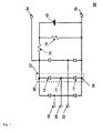
- FIG. 1 shows an exemplary first diode bridge with resistors and capacitance in a sketch 10, which corresponds to the prior art of a sum circuit.
- the diode bridge has three parallel bridge members 12, which are electrically guided with their first ends 26 to a first common output 32 and with their second ends 30 to a second common output 34th
- a bridge member 12 has two series-connected diodes 14, 16, with the electrical center 24, a respective input 18, 20, 22 of the diode bridge is connected, so that a total of three inputs result, as they are needed in a three-phase AC mains.
- a (charging) resistor 36 and a (discharge) resistor 38 are connected in series. Parallel to the (discharge) resistor 38, a capacitor 40 is connected.
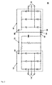
- FIG. 2 shows an exemplary inventive circuit arrangement 50.
- a first 52 and a second 60 diode bridge each with three bridge elements.
- the respective first DC side outputs 56 and 64 are electrically coupled to one another by a connection 68 and the second DC side outputs 58, 66 to a connection 70.
- the three inputs 54 of the first bridge 52 are intended to be connected to the inputs of a three-phase thyristor the three inputs of the second bridge 60 with the outputs of a three-phase Thyristorstellers.
- FIG. 3 shows an exemplary three-phase thyristor 84 according to the invention with voltage-limiting circuitry 82 in a schematic diagram 80.
- the three-phase thyristor 84 includes for each of its three phases a group 86, 88, 90 two counter-rotating thyristors 92, 94, to which a parallel connection of a resistor 96 and Capacitor 98 is provided.
- the three input and output side phases of thyristor controller 84 and circuit arrangement 82 are electrically combined at inputs 100 and outputs 102, respectively.
- an input-side supply network of, for example, 380V nominal voltage, through which the thyristor 84 is powered electrically via its inputs 100.
- the supply network can be assumed to be an ideal voltage source with a downstream network impedance.
- an output side load which is connected to the output 102 of the thyristor 84.
- a load can be broadly understood as an impedance. Both network impedance and load impedance have an influence on possible overvoltages, which are limited by the circuit arrangement 82 according to the invention.
- FIG. 4 shows in a representation 110 an exemplary single-phase thyristor with circuit arrangement and a neutral conductor 112, which is based on the basic principle of the three-phase thyristor with circuit arrangement FIG. 3 equivalent.
Landscapes
- Engineering & Computer Science (AREA)
- Power Engineering (AREA)
- Rectifiers (AREA)
Priority Applications (1)
| Application Number | Priority Date | Filing Date | Title |
|---|---|---|---|
| EP15150286.1A EP3043473B1 (fr) | 2015-01-07 | 2015-01-07 | Circuit pour variateur à thyristor |
Applications Claiming Priority (1)
| Application Number | Priority Date | Filing Date | Title |
|---|---|---|---|
| EP15150286.1A EP3043473B1 (fr) | 2015-01-07 | 2015-01-07 | Circuit pour variateur à thyristor |
Publications (2)
| Publication Number | Publication Date |
|---|---|
| EP3043473A1 true EP3043473A1 (fr) | 2016-07-13 |
| EP3043473B1 EP3043473B1 (fr) | 2022-05-18 |
Family
ID=52232096
Family Applications (1)
| Application Number | Title | Priority Date | Filing Date |
|---|---|---|---|
| EP15150286.1A Active EP3043473B1 (fr) | 2015-01-07 | 2015-01-07 | Circuit pour variateur à thyristor |
Country Status (1)
| Country | Link |
|---|---|
| EP (1) | EP3043473B1 (fr) |
Citations (7)
| Publication number | Priority date | Publication date | Assignee | Title |
|---|---|---|---|---|
| DE1538154A1 (de) * | 1966-03-29 | 1969-07-31 | Siemens Ag | Stromrichteranordnung mit Thyristoren |
| DE8716005U1 (de) * | 1987-12-03 | 1988-02-11 | Siemens AG, 1000 Berlin und 8000 München | Klemmenanschluß-Modul |
| DE19844823C1 (de) * | 1998-09-30 | 1999-10-28 | Siemens Ag | Thyristorschaltung |
| US20010026427A1 (en) * | 2000-02-08 | 2001-10-04 | Siemens Ag. | Overvoltage protection apparatus for a matrix converter |
| DE10221714A1 (de) * | 2002-05-16 | 2003-11-27 | Abb Patent Gmbh | Überspannungsschutz |
| US20060220471A1 (en) * | 2005-03-31 | 2006-10-05 | Reinhard Joho | Generator switch |
| CN101917011A (zh) * | 2010-09-06 | 2010-12-15 | 东南大学 | 用于电铁牵引供电系统的电能质量综合控制方法及装置 |
-
2015
- 2015-01-07 EP EP15150286.1A patent/EP3043473B1/fr active Active
Patent Citations (7)
| Publication number | Priority date | Publication date | Assignee | Title |
|---|---|---|---|---|
| DE1538154A1 (de) * | 1966-03-29 | 1969-07-31 | Siemens Ag | Stromrichteranordnung mit Thyristoren |
| DE8716005U1 (de) * | 1987-12-03 | 1988-02-11 | Siemens AG, 1000 Berlin und 8000 München | Klemmenanschluß-Modul |
| DE19844823C1 (de) * | 1998-09-30 | 1999-10-28 | Siemens Ag | Thyristorschaltung |
| US20010026427A1 (en) * | 2000-02-08 | 2001-10-04 | Siemens Ag. | Overvoltage protection apparatus for a matrix converter |
| DE10221714A1 (de) * | 2002-05-16 | 2003-11-27 | Abb Patent Gmbh | Überspannungsschutz |
| US20060220471A1 (en) * | 2005-03-31 | 2006-10-05 | Reinhard Joho | Generator switch |
| CN101917011A (zh) * | 2010-09-06 | 2010-12-15 | 东南大学 | 用于电铁牵引供电系统的电能质量综合控制方法及装置 |
Also Published As
| Publication number | Publication date |
|---|---|
| EP3043473B1 (fr) | 2022-05-18 |
Similar Documents
| Publication | Publication Date | Title |
|---|---|---|
| EP3895313B1 (fr) | Dispositif de commutation destiné à séparer un chemin de courant | |
| EP3853957B1 (fr) | Commutateur électronique à protection contre les surtensions | |
| EP3583670A2 (fr) | Fusible électronique pour une charge pouvant être connectée à un réseau à basse tension continue | |
| DE112016000220T5 (de) | Leistungswandlungsausrüstung | |
| EP3367567A1 (fr) | Dispositif de commutation destiné à séparer un chemin de courant | |
| EP3794730B1 (fr) | Dispositif de commutation destiné à couper un circuit de courant | |
| EP3571750B1 (fr) | Dispositif de limitation de la tension pour un réseau de tension continue | |
| DE2634667A1 (de) | Leistungssteller | |
| DE102018215881B3 (de) | Vorrichtung und Verfahren zum Koppeln zweier Gleichstromnetze | |
| EP4064563B1 (fr) | Commutateur électronique | |
| DE102013219173A1 (de) | Spannungsversorgung für elektrische Fokussierung von Elektronenstrahlen | |
| EP2845214B1 (fr) | Dispositif destiné à la commutation dans un réseau de tension continue | |
| EP2599213B1 (fr) | Système convertisseur et procédé de fonctionnement d'un système convertisseur de ce type | |
| EP3361596B1 (fr) | Batterie avec un système de gestion de batterie comprenant un dispositif interrupteur | |
| EP3895312B1 (fr) | Commutateur électronique à régulation du courant | |
| DE102019107112B3 (de) | Schaltvorrichtung, Spannungsversorgungssystem, Verfahren zum Betreiben einer Schaltvorrichtung und Herstellverfahren | |
| EP3236572A1 (fr) | Cellule de coupure d'électronique de puissance et circuit convertisseur comprenant de telles cellules de coupure | |
| EP1817828B1 (fr) | Dispositif additionnel dans un limiteur de courant pour limiter le courant en cas d'erreur | |
| EP3043473B1 (fr) | Circuit pour variateur à thyristor | |
| EP3391524B1 (fr) | Module de conversion destiné à un convertisseur multiniveaux et son procédé d'operation. | |
| DE102014212263A1 (de) | Schaltungsanordnung zur selbstregelnden Anlaufstrombegrenzung einer elektrischen Maschine | |
| DE102017106770B4 (de) | Schaltungsanordnung zum Schutz vor Netzüberspannungen für Stromrichter von Fahrzeugen, insbesondere von fahrleitungsgebundenen Fahrzeugen | |
| EP3736932A1 (fr) | Réseau de courant continu | |
| EP1619783B1 (fr) | Convertisseur avec un accroissement de la tension limité | |
| DE60013109T2 (de) | Statischer Leistungsschalter |
Legal Events
| Date | Code | Title | Description |
|---|---|---|---|
| PUAI | Public reference made under article 153(3) epc to a published international application that has entered the european phase |
Free format text: ORIGINAL CODE: 0009012 |
|
| AK | Designated contracting states |
Kind code of ref document: A1 Designated state(s): AL AT BE BG CH CY CZ DE DK EE ES FI FR GB GR HR HU IE IS IT LI LT LU LV MC MK MT NL NO PL PT RO RS SE SI SK SM TR |
|
| AX | Request for extension of the european patent |
Extension state: BA ME |
|
| STAA | Information on the status of an ep patent application or granted ep patent |
Free format text: STATUS: REQUEST FOR EXAMINATION WAS MADE |
|
| 17P | Request for examination filed |
Effective date: 20170113 |
|
| STAA | Information on the status of an ep patent application or granted ep patent |
Free format text: STATUS: EXAMINATION IS IN PROGRESS |
|
| 17Q | First examination report despatched |
Effective date: 20200102 |
|
| GRAP | Despatch of communication of intention to grant a patent |
Free format text: ORIGINAL CODE: EPIDOSNIGR1 |
|
| STAA | Information on the status of an ep patent application or granted ep patent |
Free format text: STATUS: GRANT OF PATENT IS INTENDED |
|
| INTG | Intention to grant announced |
Effective date: 20211210 |
|
| GRAS | Grant fee paid |
Free format text: ORIGINAL CODE: EPIDOSNIGR3 |
|
| GRAA | (expected) grant |
Free format text: ORIGINAL CODE: 0009210 |
|
| STAA | Information on the status of an ep patent application or granted ep patent |
Free format text: STATUS: THE PATENT HAS BEEN GRANTED |
|
| AK | Designated contracting states |
Kind code of ref document: B1 Designated state(s): AL AT BE BG CH CY CZ DE DK EE ES FI FR GB GR HR HU IE IS IT LI LT LU LV MC MK MT NL NO PL PT RO RS SE SI SK SM TR |
|
| REG | Reference to a national code |
Ref country code: GB Ref legal event code: FG4D Free format text: NOT ENGLISH |
|
| REG | Reference to a national code |
Ref country code: CH Ref legal event code: EP |
|
| REG | Reference to a national code |
Ref country code: IE Ref legal event code: FG4D Free format text: LANGUAGE OF EP DOCUMENT: GERMAN |
|
| REG | Reference to a national code |
Ref country code: DE Ref legal event code: R096 Ref document number: 502015015843 Country of ref document: DE |
|
| REG | Reference to a national code |
Ref country code: AT Ref legal event code: REF Ref document number: 1493724 Country of ref document: AT Kind code of ref document: T Effective date: 20220615 |
|
| REG | Reference to a national code |
Ref country code: LT Ref legal event code: MG9D |
|
| REG | Reference to a national code |
Ref country code: NL Ref legal event code: MP Effective date: 20220518 |
|
| PG25 | Lapsed in a contracting state [announced via postgrant information from national office to epo] |
Ref country code: SE Free format text: LAPSE BECAUSE OF FAILURE TO SUBMIT A TRANSLATION OF THE DESCRIPTION OR TO PAY THE FEE WITHIN THE PRESCRIBED TIME-LIMIT Effective date: 20220518 Ref country code: PT Free format text: LAPSE BECAUSE OF FAILURE TO SUBMIT A TRANSLATION OF THE DESCRIPTION OR TO PAY THE FEE WITHIN THE PRESCRIBED TIME-LIMIT Effective date: 20220919 Ref country code: NO Free format text: LAPSE BECAUSE OF FAILURE TO SUBMIT A TRANSLATION OF THE DESCRIPTION OR TO PAY THE FEE WITHIN THE PRESCRIBED TIME-LIMIT Effective date: 20220818 Ref country code: NL Free format text: LAPSE BECAUSE OF FAILURE TO SUBMIT A TRANSLATION OF THE DESCRIPTION OR TO PAY THE FEE WITHIN THE PRESCRIBED TIME-LIMIT Effective date: 20220518 Ref country code: LT Free format text: LAPSE BECAUSE OF FAILURE TO SUBMIT A TRANSLATION OF THE DESCRIPTION OR TO PAY THE FEE WITHIN THE PRESCRIBED TIME-LIMIT Effective date: 20220518 Ref country code: HR Free format text: LAPSE BECAUSE OF FAILURE TO SUBMIT A TRANSLATION OF THE DESCRIPTION OR TO PAY THE FEE WITHIN THE PRESCRIBED TIME-LIMIT Effective date: 20220518 Ref country code: GR Free format text: LAPSE BECAUSE OF FAILURE TO SUBMIT A TRANSLATION OF THE DESCRIPTION OR TO PAY THE FEE WITHIN THE PRESCRIBED TIME-LIMIT Effective date: 20220819 Ref country code: FI Free format text: LAPSE BECAUSE OF FAILURE TO SUBMIT A TRANSLATION OF THE DESCRIPTION OR TO PAY THE FEE WITHIN THE PRESCRIBED TIME-LIMIT Effective date: 20220518 Ref country code: ES Free format text: LAPSE BECAUSE OF FAILURE TO SUBMIT A TRANSLATION OF THE DESCRIPTION OR TO PAY THE FEE WITHIN THE PRESCRIBED TIME-LIMIT Effective date: 20220518 Ref country code: BG Free format text: LAPSE BECAUSE OF FAILURE TO SUBMIT A TRANSLATION OF THE DESCRIPTION OR TO PAY THE FEE WITHIN THE PRESCRIBED TIME-LIMIT Effective date: 20220818 |
|
| PG25 | Lapsed in a contracting state [announced via postgrant information from national office to epo] |
Ref country code: RS Free format text: LAPSE BECAUSE OF FAILURE TO SUBMIT A TRANSLATION OF THE DESCRIPTION OR TO PAY THE FEE WITHIN THE PRESCRIBED TIME-LIMIT Effective date: 20220518 Ref country code: PL Free format text: LAPSE BECAUSE OF FAILURE TO SUBMIT A TRANSLATION OF THE DESCRIPTION OR TO PAY THE FEE WITHIN THE PRESCRIBED TIME-LIMIT Effective date: 20220518 Ref country code: LV Free format text: LAPSE BECAUSE OF FAILURE TO SUBMIT A TRANSLATION OF THE DESCRIPTION OR TO PAY THE FEE WITHIN THE PRESCRIBED TIME-LIMIT Effective date: 20220518 Ref country code: IS Free format text: LAPSE BECAUSE OF FAILURE TO SUBMIT A TRANSLATION OF THE DESCRIPTION OR TO PAY THE FEE WITHIN THE PRESCRIBED TIME-LIMIT Effective date: 20220918 |
|
| PG25 | Lapsed in a contracting state [announced via postgrant information from national office to epo] |
Ref country code: SM Free format text: LAPSE BECAUSE OF FAILURE TO SUBMIT A TRANSLATION OF THE DESCRIPTION OR TO PAY THE FEE WITHIN THE PRESCRIBED TIME-LIMIT Effective date: 20220518 Ref country code: SK Free format text: LAPSE BECAUSE OF FAILURE TO SUBMIT A TRANSLATION OF THE DESCRIPTION OR TO PAY THE FEE WITHIN THE PRESCRIBED TIME-LIMIT Effective date: 20220518 Ref country code: RO Free format text: LAPSE BECAUSE OF FAILURE TO SUBMIT A TRANSLATION OF THE DESCRIPTION OR TO PAY THE FEE WITHIN THE PRESCRIBED TIME-LIMIT Effective date: 20220518 Ref country code: EE Free format text: LAPSE BECAUSE OF FAILURE TO SUBMIT A TRANSLATION OF THE DESCRIPTION OR TO PAY THE FEE WITHIN THE PRESCRIBED TIME-LIMIT Effective date: 20220518 Ref country code: DK Free format text: LAPSE BECAUSE OF FAILURE TO SUBMIT A TRANSLATION OF THE DESCRIPTION OR TO PAY THE FEE WITHIN THE PRESCRIBED TIME-LIMIT Effective date: 20220518 Ref country code: CZ Free format text: LAPSE BECAUSE OF FAILURE TO SUBMIT A TRANSLATION OF THE DESCRIPTION OR TO PAY THE FEE WITHIN THE PRESCRIBED TIME-LIMIT Effective date: 20220518 |
|
| REG | Reference to a national code |
Ref country code: DE Ref legal event code: R097 Ref document number: 502015015843 Country of ref document: DE |
|
| PLBE | No opposition filed within time limit |
Free format text: ORIGINAL CODE: 0009261 |
|
| STAA | Information on the status of an ep patent application or granted ep patent |
Free format text: STATUS: NO OPPOSITION FILED WITHIN TIME LIMIT |
|
| PG25 | Lapsed in a contracting state [announced via postgrant information from national office to epo] |
Ref country code: AL Free format text: LAPSE BECAUSE OF FAILURE TO SUBMIT A TRANSLATION OF THE DESCRIPTION OR TO PAY THE FEE WITHIN THE PRESCRIBED TIME-LIMIT Effective date: 20220518 |
|
| 26N | No opposition filed |
Effective date: 20230221 |
|
| PG25 | Lapsed in a contracting state [announced via postgrant information from national office to epo] |
Ref country code: SI Free format text: LAPSE BECAUSE OF FAILURE TO SUBMIT A TRANSLATION OF THE DESCRIPTION OR TO PAY THE FEE WITHIN THE PRESCRIBED TIME-LIMIT Effective date: 20220518 |
|
| REG | Reference to a national code |
Ref country code: CH Ref legal event code: PL |
|
| PG25 | Lapsed in a contracting state [announced via postgrant information from national office to epo] |
Ref country code: LU Free format text: LAPSE BECAUSE OF NON-PAYMENT OF DUE FEES Effective date: 20230107 |
|
| REG | Reference to a national code |
Ref country code: BE Ref legal event code: MM Effective date: 20230131 |
|
| PG25 | Lapsed in a contracting state [announced via postgrant information from national office to epo] |
Ref country code: LI Free format text: LAPSE BECAUSE OF NON-PAYMENT OF DUE FEES Effective date: 20230131 Ref country code: CH Free format text: LAPSE BECAUSE OF NON-PAYMENT OF DUE FEES Effective date: 20230131 |
|
| PG25 | Lapsed in a contracting state [announced via postgrant information from national office to epo] |
Ref country code: BE Free format text: LAPSE BECAUSE OF NON-PAYMENT OF DUE FEES Effective date: 20230131 |
|
| PG25 | Lapsed in a contracting state [announced via postgrant information from national office to epo] |
Ref country code: IT Free format text: LAPSE BECAUSE OF FAILURE TO SUBMIT A TRANSLATION OF THE DESCRIPTION OR TO PAY THE FEE WITHIN THE PRESCRIBED TIME-LIMIT Effective date: 20220518 Ref country code: IE Free format text: LAPSE BECAUSE OF NON-PAYMENT OF DUE FEES Effective date: 20230107 |
|
| REG | Reference to a national code |
Ref country code: AT Ref legal event code: MM01 Ref document number: 1493724 Country of ref document: AT Kind code of ref document: T Effective date: 20230107 |
|
| PG25 | Lapsed in a contracting state [announced via postgrant information from national office to epo] |
Ref country code: AT Free format text: LAPSE BECAUSE OF NON-PAYMENT OF DUE FEES Effective date: 20230107 |
|
| PG25 | Lapsed in a contracting state [announced via postgrant information from national office to epo] |
Ref country code: AT Free format text: LAPSE BECAUSE OF NON-PAYMENT OF DUE FEES Effective date: 20230107 |
|
| PG25 | Lapsed in a contracting state [announced via postgrant information from national office to epo] |
Ref country code: MC Free format text: LAPSE BECAUSE OF FAILURE TO SUBMIT A TRANSLATION OF THE DESCRIPTION OR TO PAY THE FEE WITHIN THE PRESCRIBED TIME-LIMIT Effective date: 20220518 |
|
| PG25 | Lapsed in a contracting state [announced via postgrant information from national office to epo] |
Ref country code: MC Free format text: LAPSE BECAUSE OF FAILURE TO SUBMIT A TRANSLATION OF THE DESCRIPTION OR TO PAY THE FEE WITHIN THE PRESCRIBED TIME-LIMIT Effective date: 20220518 |
|
| PG25 | Lapsed in a contracting state [announced via postgrant information from national office to epo] |
Ref country code: BG Free format text: LAPSE BECAUSE OF FAILURE TO SUBMIT A TRANSLATION OF THE DESCRIPTION OR TO PAY THE FEE WITHIN THE PRESCRIBED TIME-LIMIT Effective date: 20220518 |
|
| PG25 | Lapsed in a contracting state [announced via postgrant information from national office to epo] |
Ref country code: BG Free format text: LAPSE BECAUSE OF FAILURE TO SUBMIT A TRANSLATION OF THE DESCRIPTION OR TO PAY THE FEE WITHIN THE PRESCRIBED TIME-LIMIT Effective date: 20220518 |
|
| PG25 | Lapsed in a contracting state [announced via postgrant information from national office to epo] |
Ref country code: CY Free format text: LAPSE BECAUSE OF FAILURE TO SUBMIT A TRANSLATION OF THE DESCRIPTION OR TO PAY THE FEE WITHIN THE PRESCRIBED TIME-LIMIT; INVALID AB INITIO Effective date: 20150107 |
|
| PG25 | Lapsed in a contracting state [announced via postgrant information from national office to epo] |
Ref country code: HU Free format text: LAPSE BECAUSE OF FAILURE TO SUBMIT A TRANSLATION OF THE DESCRIPTION OR TO PAY THE FEE WITHIN THE PRESCRIBED TIME-LIMIT; INVALID AB INITIO Effective date: 20150107 |
|
| REG | Reference to a national code |
Ref country code: DE Ref legal event code: R082 Ref document number: 502015015843 Country of ref document: DE Representative=s name: ZIMMERMANN & PARTNER PATENTANWAELTE MBB, DE |
|
| PG25 | Lapsed in a contracting state [announced via postgrant information from national office to epo] |
Ref country code: TR Free format text: LAPSE BECAUSE OF FAILURE TO SUBMIT A TRANSLATION OF THE DESCRIPTION OR TO PAY THE FEE WITHIN THE PRESCRIBED TIME-LIMIT Effective date: 20220518 |
|
| PGFP | Annual fee paid to national office [announced via postgrant information from national office to epo] |
Ref country code: GB Payment date: 20260123 Year of fee payment: 12 |
|
| PGFP | Annual fee paid to national office [announced via postgrant information from national office to epo] |
Ref country code: DE Payment date: 20260121 Year of fee payment: 12 |
|
| PGFP | Annual fee paid to national office [announced via postgrant information from national office to epo] |
Ref country code: FR Payment date: 20260123 Year of fee payment: 12 |