EP3048743A1 - Verfahren zur steuerung der kontaktlosen kommunikation und der kontaktlosen ladung innerhalb eines systems, und entsprechendes system - Google Patents
Verfahren zur steuerung der kontaktlosen kommunikation und der kontaktlosen ladung innerhalb eines systems, und entsprechendes system Download PDFInfo
- Publication number
- EP3048743A1 EP3048743A1 EP15190537.9A EP15190537A EP3048743A1 EP 3048743 A1 EP3048743 A1 EP 3048743A1 EP 15190537 A EP15190537 A EP 15190537A EP 3048743 A1 EP3048743 A1 EP 3048743A1
- Authority
- EP
- European Patent Office
- Prior art keywords
- antenna
- communication
- control
- contactless
- ant2
- Prior art date
- Legal status (The legal status is an assumption and is not a legal conclusion. Google has not performed a legal analysis and makes no representation as to the accuracy of the status listed.)
- Granted
Links
Images

Classifications
-
- H—ELECTRICITY
- H04—ELECTRIC COMMUNICATION TECHNIQUE
- H04B—TRANSMISSION
- H04B5/00—Near-field transmission systems, e.g. inductive or capacitive transmission systems
- H04B5/70—Near-field transmission systems, e.g. inductive or capacitive transmission systems specially adapted for specific purposes
- H04B5/79—Near-field transmission systems, e.g. inductive or capacitive transmission systems specially adapted for specific purposes for data transfer in combination with power transfer
-
- H—ELECTRICITY
- H02—GENERATION; CONVERSION OR DISTRIBUTION OF ELECTRIC POWER
- H02J—ELECTRIC POWER NETWORKS; CIRCUIT ARRANGEMENTS OR SYSTEMS FOR SUPPLYING OR DISTRIBUTING ELECTRIC POWER; SYSTEMS FOR STORING ELECTRIC ENERGY
- H02J50/00—Circuit arrangements or systems for wireless supply or distribution of electric power
- H02J50/10—Circuit arrangements or systems for wireless supply or distribution of electric power using inductive coupling
- H02J50/12—Circuit arrangements or systems for wireless supply or distribution of electric power using inductive coupling of the resonant type
-
- H—ELECTRICITY
- H04—ELECTRIC COMMUNICATION TECHNIQUE
- H04B—TRANSMISSION
- H04B5/00—Near-field transmission systems, e.g. inductive or capacitive transmission systems
- H04B5/20—Near-field transmission systems, e.g. inductive or capacitive transmission systems characterised by the transmission technique; characterised by the transmission medium
- H04B5/24—Inductive coupling
- H04B5/26—Inductive coupling using coils
-
- H—ELECTRICITY
- H02—GENERATION; CONVERSION OR DISTRIBUTION OF ELECTRIC POWER
- H02J—ELECTRIC POWER NETWORKS; CIRCUIT ARRANGEMENTS OR SYSTEMS FOR SUPPLYING OR DISTRIBUTING ELECTRIC POWER; SYSTEMS FOR STORING ELECTRIC ENERGY
- H02J7/00—Circuit arrangements for charging or discharging batteries or for supplying loads from batteries
- H02J7/40—Circuit arrangements for charging or discharging batteries or for supplying loads from batteries characterised by the exchange of charge or discharge related data
- H02J7/42—Circuit arrangements for charging or discharging batteries or for supplying loads from batteries characterised by the exchange of charge or discharge related data with electronic devices having internal batteries, e.g. mobile phones
Definitions
- Embodiments and embodiments of the invention relate to the non-contact transmission of information and the charging (or recharging) without contact of a power supply module, for example a battery.
- the contactless or wireless communication is between a reader and an object, for example a transponder of the label type ("tag" in English), a contactless smart card or a mobile phone emulated in card mode without these examples are not limiting.
- the reader can also be for example a mobile phone emulated reader mode.
- Near field communication is a wireless connectivity technology that allows communication over a short distance, for example 10 cm, between electronic devices.
- electronic devices such as contactless smart cards or card-emulated smartphones, and readers.
- NFC technology is particularly suitable for connecting any type of user device and allows for quick and easy communications.
- a non-contact object is an object capable of exchanging information via an antenna with another non-contact object, for example a reader, according to a contactless communication protocol.
- An NFC object which is a contactless object, is an object compatible with NFC technology.
- NFC technology is an open standard technology platform in ISO / IEC 18092 and ISO / IEC 21481, but incorporates many existing standards such as the type A and type B protocols defined in the ISO-14443 standard which may be communication protocols that can be used in NFC technology.
- a cellular mobile phone may be used (if equipped with specific means) to exchange information with another contactless device, for example a contactless reader, using a contactless communication protocol usable in NFC technology.
- the reader When transmitting information between a reader and an emulated object in label or card mode, the reader generates a magnetic field via its antenna which is generally in the standards conventionally used, a wave at a frequency of 13. , 56MHz.
- the antenna of the object emulating the label modulates the field generated by the reader.
- This modulation is performed by modifying the load connected to the terminals of the antenna of the object.
- the output impedance of the antenna of the reader changes due to the magnetic coupling between the two antennas. This results in a change in the amplitudes and / or the phases of the voltages and currents present at the antennas of the reader and the object. And, in this way, the information to be transmitted from the object to the reader is transmitted by charge modulation to the antenna current of the reader.
- the non-contact charging technology enables contactless transfer of energy from a power source (for example a charger) to a load, for example a charging device.
- a power source for example a charger
- a load for example a charging device.
- wireless communication for example a cellular mobile phone, through the air gap separating the charger and the load.
- the Alliance for Wireless Power (A4WP) standard is one of the standards chosen by the leading manufacturers of smart cellular mobile phones (smartphones).
- the non-contact energy is transferred from a Power Transmitter Unit (PTU) and a Power Receiving Unit (PRU) which is controlled by a load management protocol.
- Non-contact energy is generated at a frequency equal to 6.78 MHz.
- a contactless communication function for example of the NFC communication type
- a charging function without contact for example in accordance with A4WP specifications.
- a method of managing the operation of a system for example incorporated within a wireless communication apparatus such as a cellular mobile phone or tablet, incorporating a communication function.
- a wireless communication apparatus such as a cellular mobile phone or tablet
- a communication function for example incorporated within a wireless communication apparatus such as a cellular mobile phone or tablet
- a power supply module such as a rechargeable battery.
- the contactless communication and the non-contact load are carried out selectively via the same antenna.
- the contactless communication function or the contactless load function is selected by configuring a matching circuit connected to the terminals of said antenna in two different ways, which makes it possible to switch frequency between the frequency used for contactless communication and the frequency used for contactless charging.
- the configuration of the matching circuit for selecting the contactless charging function also makes it possible to isolate the non-contact communication function from the antenna.
- the same means (the configurable matching circuit) is used to perform the frequency switching and to isolate from the antenna the contactless communication function when the non-contact load function is activated.
- this function when the non-contact load function is selected, this function is made operational by a configuration of a control block connected between said antenna and the power supply module, and when selecting the contactless communication function, the antenna is isolated from the non-contact load function by another configuration of the control block.
- this control block comprising for example a PMOS transistor controlled on its gate by an NMOS transistor, contributes, according to its configuration (PMOS transistor blocked or not) to make the contactless charging function operational or to isolate this function. non-contact load of the antenna when the contactless communication function is made operational.
- a system comprising an antenna, communication means configured to receive and / or transmit information via said antenna according to a contactless communication protocol, charging means configured to perform a contactless charging of a power supply module via said antenna, and control means configured to selectively operationalize the communication means or the loading means.
- control means are further configured to isolate from said antenna those of said communication means or said loading means not made operational.
- the communication means are configured to receive and / or transmit information via said antenna at a first frequency
- the loading means are configured to perform a contactless charging of the power module via said antenna to a second frequency
- the control means comprise a first configurable control block able both to select the communication means or the loading means by a frequency switching between the first and the second frequency and to isolate from said antenna the means of communication when the loading means are selected.
- the first control block comprises a configurable adaptation circuit coupled to said antenna having
- a first configuration in which it forms with said antenna a first resonant circuit having said first frequency as a resonance frequency or else it forms an impedance matching circuit compatible with the transmission / reception of information via said antenna at said first frequency
- a second configuration in which it forms with said antenna a second resonant circuit having said second frequency as resonance frequency
- the communication means comprise an input and / or output interface, and in said first configuration, the matching circuit is connected between said antenna and said input and / or output interface, and in the second configuration, the matching circuit is connected between said antenna and a cold supply point and said input and / or output interface is also connected to said cold supply point.
- the matching circuit comprises a first capacitor connected in parallel across said antenna and a plurality of second capacitors respectively connected in series between the terminals of said antenna and said input / output interface;
- the first control block further comprises a first controllable switching module connected between the input / output interface and the cold supply point and having a first state in which it prohibits an effective connection between said input interface / output and the cold supply point, the adaptation circuit being then in its first configuration, and a second state in which it actually connects said input / output interface to said cold supply point, the adaptation circuit being then in its second configuration
- the control means comprise first control means configured to selectively control said first switching module.
- the first switching module comprises a plurality of MOS transistors respectively connected between said second capacitors and said supply cold point and controllable on their respective gate by a first control signal delivered by said first control means.
- control means further comprise a second controllable and configurable control block able to make the loading means operational when the first control block has selected the loading means and to isolate the loading means from the antenna when the communication means are made operational.
- the second control block is connected between said antenna and the rechargeable power supply module and has a first state in which it prohibits an effective connection between said antenna and the power supply module, the loading means being then non-operational, and a second state in which it actually connects said antenna to said power supply module, the loading means then being made operational, and the control means comprise second control means configured to selectively control said second control block .
- the charging means comprise a rectifier bridge connected to the terminals of the antenna and a power management unit connected between the rectifier bridge and the rechargeable power supply module, and the second control block is arranged. between the rectifier bridge and the power management unit and comprises a PMOS transistor connected between an output of the rectifier bridge and the power management unit and controllable on its gate so as to be blocked in said first state and passing in said second state.
- the second control block comprises an NMOS transistor connected between the gate of the PMOS transistor and the ground and controllable by a second control signal. delivered by the second control means so as to block or turn off said PMOS transistor.
- the first control means and the second control means are combined, the first switching module and the second control block being both in their first state or in their second state.
- the communication means are communication means of the "near field communication” type and the loading means are compatible with the A4WP contactless charging technology.
- an apparatus for example a cellular mobile telephone, incorporating a system as defined above.
- the reference TEL here designates a communication device, for example a cellular mobile telephone, equipped with an antenna ANT1 for the establishment of telephone communications.
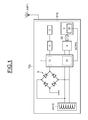
- the TEL telephone also includes here a SYS system capable, as will be seen in detail below, of performing a contactless communication function with an external device or contactless charging of a power supply module 5, for example a battery, through the same antenna ANT2, here an inductive antenna.
- a SYS system capable, as will be seen in detail below, of performing a contactless communication function with an external device or contactless charging of a power supply module 5, for example a battery, through the same antenna ANT2, here an inductive antenna.
- the antenna ANT2 can be used for communication without contact with the external device and for non-contact charging of the battery 5.
- the SYS system comprises communication means configured to receive and / or transmit information via said ANT2 antenna according to a contactless communication protocol.
- the communication means here comprise a transmission / reception device or transmission / reception head 2 of conventional structure and comprising in particular frame modulation / demodulation means, a frame controller intended in particular for calculating bits. parity according to a predefined logic function, for example that defined in ISO 14443.
- the communication means also comprise here a host microcontroller 3 connected to the device 2 by a bus 23, this host microcontroller being for example an NFC microcontroller comprising for example a conventional central unit associated with different memories.
- the battery charging means 5 here comprise a rectifier bridge 6 connected to the two terminals of the antenna ANT2 and a power management unit 4 (known to those skilled in the art under the acronym "PMU"). Power Management Unit) connected between the rectifier bridge 6 and the rechargeable battery 5.
- PMU power management unit
- the SYS system also comprises control means configured to selectively make operational the communication means or the loading means.
- control means further configured to isolate ANT2 antenna those means of communication or loading means that are not made operational.
- control means comprise, as illustrated on the figure 1 , a stage 1 comprising a first control block 10 and a second control block 12, these two control blocks being configurable and controllable by means of a control signal SCTRL delivered by control means 30 located here in the microcontroller 3 and made for example in software form.
- control means 30 located here in the microcontroller 3 and made for example in software form.
- these control means could be arranged in the radiofrequency head 2.
- the radiofrequency head 2 could also incorporate the stage 1 and the rectifier bridge 6 dedicated to the non-contact load.
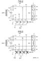
- the first control block 10 includes ( figure 2 ) a configurable adaptation circuit 100 coupled to the two terminals AC0 and AC1 of the antenna ANT2.
- the transmitting / receiving head 2 comprises an input and / or output interface having here two contacts T20 and T21 that can be used in reader mode and two other contacts R20 and R21 usable in reader mode and card mode.
- the head 2 is advantageously equipped with an internal switch SW making it possible to short-circuit the contacts T20 and T21 for operation in card mode, or to not short-circuit the contacts to allow operation in reader mode. .
- the matching circuit here comprises a first capacitor Cp connected in parallel to the terminals AC0 and AC1 of the antenna ANT2 as well as the contacts T20 and T21.
- the matching circuit also has second capacitors Cs and Crx.
- a second capacitor Cs is connected in series between the terminal AC0 and the contact T20.
- Another second capacitor Cs is connected in series between the terminal AC1 and the contact T21.
- Two other second capacitors Crx are connected in series respectively between the terminals AC0, AC1 and the contacts R20 and R21.
- the first control block 10 also comprises a first switching module 110 controllable by the control signal SCTRL.
- This first switching block here comprises four NMOS transistors T1-T4 respectively connected between the terminals B1-B4 of the capacitors Cs and Crx and a cold supply point, here GND.
- the gates of these NMOS transistors are controllable by the control signal SCTRL.
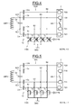
- This adaptation circuit 100 can take different configurations as illustrated on the Figures 3 to 5 .
- control signal SCTRL is in the logic state 0 corresponding to a selection of the contactless communication function and to a first state 110A of the first switching module 100.
- the transistors T1 to T4 are blocked and the matching circuit 100 then forms with the antenna ANT2 a resonant circuit 100A. More precisely, the capacitors Cp and Cs form at the terminals of the antenna an equivalent capacitor Ct whose value is equal to Cp + Cs / 2. For the purpose of simplification Ct, Cp and Cs designate both the corresponding capacitors and their capacitive values.
- the capacitive values Cp and Cs are chosen so that the resonant circuit has a first resonant frequency f equal to 13.56 MHz.
- the first switching module 110 is always in its first state 110A corresponding to the logic value 0 of the signal SCTRL.
- the internal switch SW is open, which corresponds to the use of the communication means in reader mode.
- the matching circuit in its first configuration, forms an impedance matching circuit 100B compatible with the transmission / reception of information via the antenna ANT2 at the first frequency f.
- the impedance matching circuit makes it possible to obtain an impedance seen from the contacts T20 and T21 which is the complex conjugate of the impedance of the antenna ANT2.
- the first switching block 110 goes into a second state 110C in which the transistors T1 to T4 are on.
- the terminals B1 to B4 are connected to ground and the matching circuit forms, at the terminals AC0 and AC1 of the antenna ANT2, a capacitive circuit having a capacitive value equal to Ct + Crx / 2.
- Crx refers to both the corresponding capacitor and its capacitive value.
- This capacitive circuit forms with the antenna ANT2 a resonant circuit and by choosing a capacitive value of the capacitors Crx equal to six times the value Ct, this resonant circuit will have a second resonance frequency equal to 6.78 MHz, which is compatible with non-contact charging that complies with the A4WP specifications.
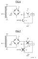
- this second control block 12 comprises a PMOS transistor T6 connected in series between an output of the rectifier bridge 6 and the power management unit 4. Moreover, a resistor R6 is connected between the output of the rectifier bridge and the gate of transistor T6.
- This second control block also comprises an NMOS transistor T7 connected between the gate of the PMOS transistor T6 and the ground GND.
- This NMOS transistor T7 is controlled on its gate by the control signal SCTRL.
- the loading means 4 are then non-operational since there is no effective connection between the antenna ANT2 and the power supply module (battery).
- the loading means are then effectively isolated from the antenna ANT2 and do not disturb the operation of the contactless communication.
- the NMOS transistor T7 is on, which turns on the PMOS transistor T6 and effectively connects the power management unit 4 to the rectifier bridge 6 and therefore to the antenna ANT2.
- the loading means are then made operational.
Landscapes
- Engineering & Computer Science (AREA)
- Computer Networks & Wireless Communication (AREA)
- Signal Processing (AREA)
- Power Engineering (AREA)
- Charge And Discharge Circuits For Batteries Or The Like (AREA)
- Near-Field Transmission Systems (AREA)
Applications Claiming Priority (1)
| Application Number | Priority Date | Filing Date | Title |
|---|---|---|---|
| FR1550566A FR3032076A1 (fr) | 2015-01-26 | 2015-01-26 | Procede de gestion de la communication sans contact et de la charge sans contact au sein d'un systeme, et systeme correspondant |
Publications (2)
| Publication Number | Publication Date |
|---|---|
| EP3048743A1 true EP3048743A1 (de) | 2016-07-27 |
| EP3048743B1 EP3048743B1 (de) | 2020-07-01 |
Family
ID=53269643
Family Applications (1)
| Application Number | Title | Priority Date | Filing Date |
|---|---|---|---|
| EP15190537.9A Active EP3048743B1 (de) | 2015-01-26 | 2015-10-20 | Verfahren zur steuerung der kontaktlosen kommunikation und der kontaktlosen ladung innerhalb eines systems, und entsprechendes system |
Country Status (4)
| Country | Link |
|---|---|
| US (2) | US9887741B2 (de) |
| EP (1) | EP3048743B1 (de) |
| CN (3) | CN205249222U (de) |
| FR (1) | FR3032076A1 (de) |
Families Citing this family (6)
| Publication number | Priority date | Publication date | Assignee | Title |
|---|---|---|---|---|
| FR3032076A1 (fr) | 2015-01-26 | 2016-07-29 | Stmicroelectronics Rousset | Procede de gestion de la communication sans contact et de la charge sans contact au sein d'un systeme, et systeme correspondant |
| FR3062937A1 (fr) * | 2017-02-14 | 2018-08-17 | Stmicroelectronics (Rousset) Sas | Activation d'un dispositif nfc |
| US10997483B2 (en) | 2019-06-12 | 2021-05-04 | Stmicroelectronics, Inc | NFC antenna switch |
| CN113131621A (zh) * | 2020-01-14 | 2021-07-16 | 北京小米移动软件有限公司 | 无线充电方法及装置、终端设备、充电系统、存储介质 |
| FR3119058B1 (fr) | 2021-01-15 | 2023-03-31 | St Microelectronics Rousset | Gestion de la communication sans contact et du chargement sans contact à partir d’un dispositif sans contact, et dispositif sans contact correspondant |
| CN114765466B (zh) * | 2021-01-15 | 2024-06-21 | 意法半导体(鲁塞)公司 | 管理非接触式通信和非接触式充电以及相应非接触式设备 |
Citations (2)
| Publication number | Priority date | Publication date | Assignee | Title |
|---|---|---|---|---|
| WO2010035256A2 (en) * | 2008-09-23 | 2010-04-01 | Powermat Ltd. | Combined antenna and inductive power receiver |
| US20120149301A1 (en) * | 2010-12-13 | 2012-06-14 | Qualcomm Incorporated | Receiver for near field communication and wireless power functionalities |
Family Cites Families (13)
| Publication number | Priority date | Publication date | Assignee | Title |
|---|---|---|---|---|
| JP4101816B2 (ja) * | 2005-05-16 | 2008-06-18 | 日本テキサス・インスツルメンツ株式会社 | バッテリ保護回路 |
| EP2648135B1 (de) * | 2010-11-29 | 2019-07-17 | Fujitsu Limited | Tragbare vorrichtung und stromversorgungssystem |
| FR2971378B1 (fr) * | 2011-02-04 | 2013-02-22 | St Microelectronics Rousset | Procede de connexion sur une seule antenne d'un ou de plusieurs composants sans contact, et systeme correspondant |
| JP5677875B2 (ja) * | 2011-03-16 | 2015-02-25 | 日立マクセル株式会社 | 非接触電力伝送システム |
| FR2987475B1 (fr) * | 2012-02-24 | 2016-07-08 | Stmicroelectronics Rousset | Recharge d'un dispositif nfc |
| CN106887883B (zh) * | 2012-02-29 | 2019-08-23 | 松下知识产权经营株式会社 | 充电装置 |
| JP2014023281A (ja) * | 2012-07-18 | 2014-02-03 | Panasonic Corp | 伝送コイル装置及び携帯無線端末 |
| US8977197B2 (en) * | 2012-10-11 | 2015-03-10 | Qualcomm Incorporated | Circuit tuning for device detection in near-field communications |
| CN103117813A (zh) | 2012-10-18 | 2013-05-22 | 中兴通讯股份有限公司 | 一种用户终端以及控制nfc单元与无线充电单元切换的方法 |
| KR102072522B1 (ko) | 2013-03-07 | 2020-02-03 | 삼성전자주식회사 | 비접촉 통신 장치 및 그것을 포함한 유저 장치 |
| WO2014199507A1 (ja) * | 2013-06-14 | 2014-12-18 | ルネサスエレクトロニクス株式会社 | 通信制御装置及び実装基板 |
| CN103441581B (zh) * | 2013-08-19 | 2015-06-17 | 广西电网公司电力科学研究院 | 一种基于可控电感的ipt系统原边功率调节方法及系统 |
| FR3032076A1 (fr) | 2015-01-26 | 2016-07-29 | Stmicroelectronics Rousset | Procede de gestion de la communication sans contact et de la charge sans contact au sein d'un systeme, et systeme correspondant |
-
2015
- 2015-01-26 FR FR1550566A patent/FR3032076A1/fr active Pending
- 2015-10-13 US US14/881,528 patent/US9887741B2/en not_active Expired - Fee Related
- 2015-10-20 EP EP15190537.9A patent/EP3048743B1/de active Active
- 2015-11-20 CN CN201520935152.0U patent/CN205249222U/zh not_active Expired - Lifetime
- 2015-11-20 CN CN201510811509.9A patent/CN105827278B/zh active Active
- 2015-11-20 CN CN201910312816.0A patent/CN109980759B/zh active Active
-
2017
- 2017-12-18 US US15/845,632 patent/US10432268B2/en active Active
Patent Citations (2)
| Publication number | Priority date | Publication date | Assignee | Title |
|---|---|---|---|---|
| WO2010035256A2 (en) * | 2008-09-23 | 2010-04-01 | Powermat Ltd. | Combined antenna and inductive power receiver |
| US20120149301A1 (en) * | 2010-12-13 | 2012-06-14 | Qualcomm Incorporated | Receiver for near field communication and wireless power functionalities |
Non-Patent Citations (2)
| Title |
|---|
| "Introduction to the Alliance for Wireless Power Loosely-Coupled Wireless Power Transfer System Specification Version 1.0", IEEE WIRELESS POWER TRANSFER CONFERENCE 2013, TECHNOLOGIES, SYSTEMS AND APPLICATIONS, MAY 15-16 2013, 15 May 2013 (2013-05-15) |
| RYAN TSENG ET AL: "Introduction to the alliance for wireless power loosely-coupled wireless power transfer system specification version 1.0", 2013 IEEE WIRELESS POWER TRANSFER (WPT), 1 May 2013 (2013-05-01), pages 79 - 83, XP055228583, ISBN: 978-1-4673-5009-9, DOI: 10.1109/WPT.2013.6556887 * |
Also Published As
| Publication number | Publication date |
|---|---|
| US20160218774A1 (en) | 2016-07-28 |
| EP3048743B1 (de) | 2020-07-01 |
| US9887741B2 (en) | 2018-02-06 |
| US20180109294A1 (en) | 2018-04-19 |
| CN205249222U (zh) | 2016-05-18 |
| CN109980759B (zh) | 2023-04-18 |
| FR3032076A1 (fr) | 2016-07-29 |
| CN105827278A (zh) | 2016-08-03 |
| US10432268B2 (en) | 2019-10-01 |
| CN109980759A (zh) | 2019-07-05 |
| CN105827278B (zh) | 2019-05-28 |
Similar Documents
| Publication | Publication Date | Title |
|---|---|---|
| EP3048743B1 (de) | Verfahren zur steuerung der kontaktlosen kommunikation und der kontaktlosen ladung innerhalb eines systems, und entsprechendes system | |
| EP2341469B1 (de) | Elektronisches System und Verfahren zum Management von konkurrierenden kontaktlosen Kommunikationen im System | |
| EP2485396B1 (de) | Verfahren zum Anschluss einer oder mehreren kontaktlosen Komponenten auf einer einzigen Antenne, und entsprechendes System | |
| EP3001575B1 (de) | Verfahren zur steuerung des betriebs eines objekts, das in der lage ist, ohne einen kontakt mit einem lesegerät zu kommunizieren, entsprechende vorrichtung und entsprechendes objekt | |
| EP3101816B1 (de) | System und vorrichtung zur steuerung der abstimmung auf eine kommunikationsfrequenz einer antenne, die mit einer komponente verbunden ist, die für eine kontaktlose kommunikation ausgelegt ist. | |
| EP2792017B1 (de) | Antennenvorrichtung und antennenkonfigurationsverfahren | |
| EP3054393B1 (de) | Authentifizierungsverfahren eines objekts mit hilfe einer vorrichtung, die jeweils in der lage sind, kontaktlos untereinander zu kommunizieren, sowie entsprechendes system und objekt | |
| EP3301608B1 (de) | Methode zur anwesenheitsdetektion von objekten für einen kabellosen leser und entsprechender leser | |
| EP3012980B1 (de) | Verfahren zur steuerung des betriebs, insbesondere der belastungsmodulation, eines objekts, das in der lage ist, kontaktlos mit einem lesegerät zu kommunizieren, entsprechende vorrichtung und entsprechendes objekt | |
| EP3648362B1 (de) | Verfahren zur beschränkung des über einen transponder empfangenen spannungsniveaus aus einem magnetfeld, und entsprechender transponder | |
| EP2582113A1 (de) | Adaptationsvorrichtung zwischen einem kontaktlosen Lesegerät und einem Funkgerät | |
| FR3119058A1 (fr) | Gestion de la communication sans contact et du chargement sans contact à partir d’un dispositif sans contact, et dispositif sans contact correspondant | |
| FR2982686A1 (fr) | Protection d'un terminal d'emission-reception radio-frequence contre des perturbations electromagnetiques | |
| EP2999130B1 (de) | Kontaktloses kommunikationsverfahren zwischen zwei nfc-geräten mit reduzierung des einflusses einer externen lärmemission | |
| EP2372613A1 (de) | Funkkommunikationsgegenstand mit doppelter Reichweite, und Umsetzungsverfahren | |
| FR3085551A1 (fr) | Protection d'un transpondeur passif soumis a un champ magnetique genere par exemple par un chargeur sans contact | |
| FR3103597A1 (fr) | Procédé de contrôle du positionnement relatif de deux objets et système correspondant | |
| EP1580834B1 (de) | System und Verfahren zur dynamischen Kontrolle der Bandbreite einer Antenne, zugehöriges Telefon | |
| EP2401706B1 (de) | Tragbare vorrichtung, insbesondere usb-flash-laufwerk, die mit mehreren wählbaren kontaktlosen kommunikationsschnittstellen versehen ist | |
| EP2570973A1 (de) | Verfahren zur Herstellung einer drahtlosen Kommunikation und zugehörige Chipkarte | |
| FR3159867A1 (fr) | Contrôleur NFC | |
| FR3008247A1 (fr) | Procede et dispositif de charge par couplage magnetique pour vehicule automobile |
Legal Events
| Date | Code | Title | Description |
|---|---|---|---|
| PUAI | Public reference made under article 153(3) epc to a published international application that has entered the european phase |
Free format text: ORIGINAL CODE: 0009012 |
|
| 17P | Request for examination filed |
Effective date: 20151020 |
|
| AK | Designated contracting states |
Kind code of ref document: A1 Designated state(s): AL AT BE BG CH CY CZ DE DK EE ES FI FR GB GR HR HU IE IS IT LI LT LU LV MC MK MT NL NO PL PT RO RS SE SI SK SM TR |
|
| AX | Request for extension of the european patent |
Extension state: BA ME |
|
| STAA | Information on the status of an ep patent application or granted ep patent |
Free format text: STATUS: EXAMINATION IS IN PROGRESS |
|
| 17Q | First examination report despatched |
Effective date: 20180118 |
|
| GRAP | Despatch of communication of intention to grant a patent |
Free format text: ORIGINAL CODE: EPIDOSNIGR1 |
|
| STAA | Information on the status of an ep patent application or granted ep patent |
Free format text: STATUS: GRANT OF PATENT IS INTENDED |
|
| RIC1 | Information provided on ipc code assigned before grant |
Ipc: H02J 50/12 20160101ALI20191119BHEP Ipc: H04B 5/00 20060101AFI20191119BHEP Ipc: H02J 7/02 20160101ALI20191119BHEP |
|
| INTG | Intention to grant announced |
Effective date: 20191217 |
|
| RIN1 | Information on inventor provided before grant (corrected) |
Inventor name: TORNAMBE, ANTHONY Inventor name: RIZZO, PIERRE |
|
| GRAS | Grant fee paid |
Free format text: ORIGINAL CODE: EPIDOSNIGR3 |
|
| GRAJ | Information related to disapproval of communication of intention to grant by the applicant or resumption of examination proceedings by the epo deleted |
Free format text: ORIGINAL CODE: EPIDOSDIGR1 |
|
| GRAL | Information related to payment of fee for publishing/printing deleted |
Free format text: ORIGINAL CODE: EPIDOSDIGR3 |
|
| STAA | Information on the status of an ep patent application or granted ep patent |
Free format text: STATUS: EXAMINATION IS IN PROGRESS |
|
| INTC | Intention to grant announced (deleted) | ||
| GRAR | Information related to intention to grant a patent recorded |
Free format text: ORIGINAL CODE: EPIDOSNIGR71 |
|
| STAA | Information on the status of an ep patent application or granted ep patent |
Free format text: STATUS: GRANT OF PATENT IS INTENDED |
|
| GRAA | (expected) grant |
Free format text: ORIGINAL CODE: 0009210 |
|
| STAA | Information on the status of an ep patent application or granted ep patent |
Free format text: STATUS: THE PATENT HAS BEEN GRANTED |
|
| INTG | Intention to grant announced |
Effective date: 20200520 |
|
| AK | Designated contracting states |
Kind code of ref document: B1 Designated state(s): AL AT BE BG CH CY CZ DE DK EE ES FI FR GB GR HR HU IE IS IT LI LT LU LV MC MK MT NL NO PL PT RO RS SE SI SK SM TR |
|
| REG | Reference to a national code |
Ref country code: CH Ref legal event code: EP Ref country code: AT Ref legal event code: REF Ref document number: 1287148 Country of ref document: AT Kind code of ref document: T Effective date: 20200715 |
|
| REG | Reference to a national code |
Ref country code: IE Ref legal event code: FG4D Free format text: LANGUAGE OF EP DOCUMENT: FRENCH |
|
| REG | Reference to a national code |
Ref country code: DE Ref legal event code: R096 Ref document number: 602015054998 Country of ref document: DE |
|
| PGFP | Annual fee paid to national office [announced via postgrant information from national office to epo] |
Ref country code: FR Payment date: 20200917 Year of fee payment: 6 |
|
| REG | Reference to a national code |
Ref country code: LT Ref legal event code: MG4D |
|
| PG25 | Lapsed in a contracting state [announced via postgrant information from national office to epo] |
Ref country code: BG Free format text: LAPSE BECAUSE OF FAILURE TO SUBMIT A TRANSLATION OF THE DESCRIPTION OR TO PAY THE FEE WITHIN THE PRESCRIBED TIME-LIMIT Effective date: 20201001 |
|
| REG | Reference to a national code |
Ref country code: NL Ref legal event code: MP Effective date: 20200701 |
|
| REG | Reference to a national code |
Ref country code: AT Ref legal event code: MK05 Ref document number: 1287148 Country of ref document: AT Kind code of ref document: T Effective date: 20200701 |
|
| PG25 | Lapsed in a contracting state [announced via postgrant information from national office to epo] |
Ref country code: SE Free format text: LAPSE BECAUSE OF FAILURE TO SUBMIT A TRANSLATION OF THE DESCRIPTION OR TO PAY THE FEE WITHIN THE PRESCRIBED TIME-LIMIT Effective date: 20200701 Ref country code: NO Free format text: LAPSE BECAUSE OF FAILURE TO SUBMIT A TRANSLATION OF THE DESCRIPTION OR TO PAY THE FEE WITHIN THE PRESCRIBED TIME-LIMIT Effective date: 20201001 Ref country code: HR Free format text: LAPSE BECAUSE OF FAILURE TO SUBMIT A TRANSLATION OF THE DESCRIPTION OR TO PAY THE FEE WITHIN THE PRESCRIBED TIME-LIMIT Effective date: 20200701 Ref country code: AT Free format text: LAPSE BECAUSE OF FAILURE TO SUBMIT A TRANSLATION OF THE DESCRIPTION OR TO PAY THE FEE WITHIN THE PRESCRIBED TIME-LIMIT Effective date: 20200701 Ref country code: GR Free format text: LAPSE BECAUSE OF FAILURE TO SUBMIT A TRANSLATION OF THE DESCRIPTION OR TO PAY THE FEE WITHIN THE PRESCRIBED TIME-LIMIT Effective date: 20201002 Ref country code: FI Free format text: LAPSE BECAUSE OF FAILURE TO SUBMIT A TRANSLATION OF THE DESCRIPTION OR TO PAY THE FEE WITHIN THE PRESCRIBED TIME-LIMIT Effective date: 20200701 Ref country code: ES Free format text: LAPSE BECAUSE OF FAILURE TO SUBMIT A TRANSLATION OF THE DESCRIPTION OR TO PAY THE FEE WITHIN THE PRESCRIBED TIME-LIMIT Effective date: 20200701 Ref country code: LT Free format text: LAPSE BECAUSE OF FAILURE TO SUBMIT A TRANSLATION OF THE DESCRIPTION OR TO PAY THE FEE WITHIN THE PRESCRIBED TIME-LIMIT Effective date: 20200701 Ref country code: PT Free format text: LAPSE BECAUSE OF FAILURE TO SUBMIT A TRANSLATION OF THE DESCRIPTION OR TO PAY THE FEE WITHIN THE PRESCRIBED TIME-LIMIT Effective date: 20201102 Ref country code: CZ Free format text: LAPSE BECAUSE OF FAILURE TO SUBMIT A TRANSLATION OF THE DESCRIPTION OR TO PAY THE FEE WITHIN THE PRESCRIBED TIME-LIMIT Effective date: 20200701 |
|
| PG25 | Lapsed in a contracting state [announced via postgrant information from national office to epo] |
Ref country code: LV Free format text: LAPSE BECAUSE OF FAILURE TO SUBMIT A TRANSLATION OF THE DESCRIPTION OR TO PAY THE FEE WITHIN THE PRESCRIBED TIME-LIMIT Effective date: 20200701 Ref country code: PL Free format text: LAPSE BECAUSE OF FAILURE TO SUBMIT A TRANSLATION OF THE DESCRIPTION OR TO PAY THE FEE WITHIN THE PRESCRIBED TIME-LIMIT Effective date: 20200701 Ref country code: RS Free format text: LAPSE BECAUSE OF FAILURE TO SUBMIT A TRANSLATION OF THE DESCRIPTION OR TO PAY THE FEE WITHIN THE PRESCRIBED TIME-LIMIT Effective date: 20200701 Ref country code: IS Free format text: LAPSE BECAUSE OF FAILURE TO SUBMIT A TRANSLATION OF THE DESCRIPTION OR TO PAY THE FEE WITHIN THE PRESCRIBED TIME-LIMIT Effective date: 20201101 |
|
| PG25 | Lapsed in a contracting state [announced via postgrant information from national office to epo] |
Ref country code: NL Free format text: LAPSE BECAUSE OF FAILURE TO SUBMIT A TRANSLATION OF THE DESCRIPTION OR TO PAY THE FEE WITHIN THE PRESCRIBED TIME-LIMIT Effective date: 20200701 |
|
| REG | Reference to a national code |
Ref country code: DE Ref legal event code: R097 Ref document number: 602015054998 Country of ref document: DE |
|
| PG25 | Lapsed in a contracting state [announced via postgrant information from national office to epo] |
Ref country code: DK Free format text: LAPSE BECAUSE OF FAILURE TO SUBMIT A TRANSLATION OF THE DESCRIPTION OR TO PAY THE FEE WITHIN THE PRESCRIBED TIME-LIMIT Effective date: 20200701 Ref country code: IT Free format text: LAPSE BECAUSE OF FAILURE TO SUBMIT A TRANSLATION OF THE DESCRIPTION OR TO PAY THE FEE WITHIN THE PRESCRIBED TIME-LIMIT Effective date: 20200701 Ref country code: RO Free format text: LAPSE BECAUSE OF FAILURE TO SUBMIT A TRANSLATION OF THE DESCRIPTION OR TO PAY THE FEE WITHIN THE PRESCRIBED TIME-LIMIT Effective date: 20200701 Ref country code: SM Free format text: LAPSE BECAUSE OF FAILURE TO SUBMIT A TRANSLATION OF THE DESCRIPTION OR TO PAY THE FEE WITHIN THE PRESCRIBED TIME-LIMIT Effective date: 20200701 Ref country code: EE Free format text: LAPSE BECAUSE OF FAILURE TO SUBMIT A TRANSLATION OF THE DESCRIPTION OR TO PAY THE FEE WITHIN THE PRESCRIBED TIME-LIMIT Effective date: 20200701 |
|
| PLBE | No opposition filed within time limit |
Free format text: ORIGINAL CODE: 0009261 |
|
| STAA | Information on the status of an ep patent application or granted ep patent |
Free format text: STATUS: NO OPPOSITION FILED WITHIN TIME LIMIT |
|
| PG25 | Lapsed in a contracting state [announced via postgrant information from national office to epo] |
Ref country code: AL Free format text: LAPSE BECAUSE OF FAILURE TO SUBMIT A TRANSLATION OF THE DESCRIPTION OR TO PAY THE FEE WITHIN THE PRESCRIBED TIME-LIMIT Effective date: 20200701 |
|
| REG | Reference to a national code |
Ref country code: CH Ref legal event code: PL |
|
| 26N | No opposition filed |
Effective date: 20210406 |
|
| GBPC | Gb: european patent ceased through non-payment of renewal fee |
Effective date: 20201020 |
|
| PG25 | Lapsed in a contracting state [announced via postgrant information from national office to epo] |
Ref country code: LU Free format text: LAPSE BECAUSE OF NON-PAYMENT OF DUE FEES Effective date: 20201020 Ref country code: MC Free format text: LAPSE BECAUSE OF FAILURE TO SUBMIT A TRANSLATION OF THE DESCRIPTION OR TO PAY THE FEE WITHIN THE PRESCRIBED TIME-LIMIT Effective date: 20200701 Ref country code: SK Free format text: LAPSE BECAUSE OF FAILURE TO SUBMIT A TRANSLATION OF THE DESCRIPTION OR TO PAY THE FEE WITHIN THE PRESCRIBED TIME-LIMIT Effective date: 20200701 |
|
| REG | Reference to a national code |
Ref country code: BE Ref legal event code: MM Effective date: 20201031 |
|
| PG25 | Lapsed in a contracting state [announced via postgrant information from national office to epo] |
Ref country code: SI Free format text: LAPSE BECAUSE OF FAILURE TO SUBMIT A TRANSLATION OF THE DESCRIPTION OR TO PAY THE FEE WITHIN THE PRESCRIBED TIME-LIMIT Effective date: 20200701 Ref country code: GB Free format text: LAPSE BECAUSE OF NON-PAYMENT OF DUE FEES Effective date: 20201020 Ref country code: LI Free format text: LAPSE BECAUSE OF NON-PAYMENT OF DUE FEES Effective date: 20201031 Ref country code: BE Free format text: LAPSE BECAUSE OF NON-PAYMENT OF DUE FEES Effective date: 20201031 Ref country code: CH Free format text: LAPSE BECAUSE OF NON-PAYMENT OF DUE FEES Effective date: 20201031 |
|
| PG25 | Lapsed in a contracting state [announced via postgrant information from national office to epo] |
Ref country code: IE Free format text: LAPSE BECAUSE OF NON-PAYMENT OF DUE FEES Effective date: 20201020 |
|
| PG25 | Lapsed in a contracting state [announced via postgrant information from national office to epo] |
Ref country code: TR Free format text: LAPSE BECAUSE OF FAILURE TO SUBMIT A TRANSLATION OF THE DESCRIPTION OR TO PAY THE FEE WITHIN THE PRESCRIBED TIME-LIMIT Effective date: 20200701 Ref country code: MT Free format text: LAPSE BECAUSE OF FAILURE TO SUBMIT A TRANSLATION OF THE DESCRIPTION OR TO PAY THE FEE WITHIN THE PRESCRIBED TIME-LIMIT Effective date: 20200701 Ref country code: CY Free format text: LAPSE BECAUSE OF FAILURE TO SUBMIT A TRANSLATION OF THE DESCRIPTION OR TO PAY THE FEE WITHIN THE PRESCRIBED TIME-LIMIT Effective date: 20200701 |
|
| PG25 | Lapsed in a contracting state [announced via postgrant information from national office to epo] |
Ref country code: MK Free format text: LAPSE BECAUSE OF FAILURE TO SUBMIT A TRANSLATION OF THE DESCRIPTION OR TO PAY THE FEE WITHIN THE PRESCRIBED TIME-LIMIT Effective date: 20200701 |
|
| PG25 | Lapsed in a contracting state [announced via postgrant information from national office to epo] |
Ref country code: FR Free format text: LAPSE BECAUSE OF NON-PAYMENT OF DUE FEES Effective date: 20211031 |
|
| PGFP | Annual fee paid to national office [announced via postgrant information from national office to epo] |
Ref country code: DE Payment date: 20240919 Year of fee payment: 10 |