EP3101816B1 - System und vorrichtung zur steuerung der abstimmung auf eine kommunikationsfrequenz einer antenne, die mit einer komponente verbunden ist, die für eine kontaktlose kommunikation ausgelegt ist. - Google Patents
System und vorrichtung zur steuerung der abstimmung auf eine kommunikationsfrequenz einer antenne, die mit einer komponente verbunden ist, die für eine kontaktlose kommunikation ausgelegt ist. Download PDFInfo
- Publication number
- EP3101816B1 EP3101816B1 EP15190532.0A EP15190532A EP3101816B1 EP 3101816 B1 EP3101816 B1 EP 3101816B1 EP 15190532 A EP15190532 A EP 15190532A EP 3101816 B1 EP3101816 B1 EP 3101816B1
- Authority
- EP
- European Patent Office
- Prior art keywords
- capacitive
- auxiliary
- antenna
- terminals
- configurable
- Prior art date
- Legal status (The legal status is an assumption and is not a legal conclusion. Google has not performed a legal analysis and makes no representation as to the accuracy of the status listed.)
- Active
Links
Images


Classifications
-
- H—ELECTRICITY
- H04—ELECTRIC COMMUNICATION TECHNIQUE
- H04B—TRANSMISSION
- H04B5/00—Near-field transmission systems, e.g. inductive or capacitive transmission systems
- H04B5/70—Near-field transmission systems, e.g. inductive or capacitive transmission systems specially adapted for specific purposes
-
- H—ELECTRICITY
- H04—ELECTRIC COMMUNICATION TECHNIQUE
- H04B—TRANSMISSION
- H04B1/00—Details of transmission systems, not covered by a single one of groups H04B3/00 - H04B13/00; Details of transmission systems not characterised by the medium used for transmission
- H04B1/38—Transceivers, i.e. devices in which transmitter and receiver form a structural unit and in which at least one part is used for functions of transmitting and receiving
- H04B1/40—Circuits
-
- H—ELECTRICITY
- H04—ELECTRIC COMMUNICATION TECHNIQUE
- H04B—TRANSMISSION
- H04B1/00—Details of transmission systems, not covered by a single one of groups H04B3/00 - H04B13/00; Details of transmission systems not characterised by the medium used for transmission
- H04B1/06—Receivers
- H04B1/16—Circuits
- H04B1/18—Input circuits, e.g. for coupling to an antenna or a transmission line
-
- H—ELECTRICITY
- H04—ELECTRIC COMMUNICATION TECHNIQUE
- H04B—TRANSMISSION
- H04B1/00—Details of transmission systems, not covered by a single one of groups H04B3/00 - H04B13/00; Details of transmission systems not characterised by the medium used for transmission
- H04B1/02—Transmitters
- H04B1/04—Circuits
- H04B1/0458—Arrangements for matching and coupling between power amplifier and antenna or between amplifying stages
Definitions
- Modes of implementation and embodiments of the invention relate to wireless or contactless communication using electronic components connected to an antenna, in particular components configured to exchange information with an external device via said antenna according to a communication protocol of the contactless type and more particularly the control of a frequency tuning of the antenna, that is to say a tuning of the antenna on a frequency compatible with a contactless communication of information.
- a frequency may for example be a resonance frequency equal to a carrier frequency, for example 13.56 MHz, or else a resonance frequency contained in an admissible range around the carrier frequency.
- Such components are more simply called, by abuse of language “contactless components” and can be for example so-called “NFC” components, that is to say components compatible with NFC technology ("Near Field Communication”) .
- the NFC component can for example be an NFC microcontroller.
- NFC Near Field Communication
- NFC technology is standardized in ISO/IEC 18092 and ISO/IEC 21481 but incorporates a variety of pre-existing standards including Type A and Type B protocols from ISO/IEC 14443.
- Type A and Type B protocols from ISO/IEC 14443.
- a prior art example may to be found in US 2014/106668A1 .
- An NFC microcontroller can generally be used either in “reader” mode or in “card” mode, to dialogue with another contactless device, for example by using a communication protocol.
- contactless communication such as the type A protocol of the ISO/IEC 14 443 standard.
- the NFC component acts as a reader vis-à-vis the external contactless device which can then be a card or a tag.
- the NFC component can then read the content of the external device and write information to the external device.
- the NFC component In the “card” mode, the NFC component then behaves like a card or a tag and dialogues with the external device which this time is a reader.
- An NFC microcontroller can for example be incorporated into a cellular mobile telephone, and the latter can then be used, in addition to its conventional telephone function, to exchange information with the external contactless device.
- Contactless components such as NFC components
- these external components used in this impedance matching circuit for example coils and capacitors, must be very well dimensioned, so as to allow good frequency tuning of the antenna, for example on a carrier frequency, (for example 13.56 MHz), and thus ensure maximum performance.
- This frequency mismatch of the antenna can also be caused by the magnetic coupling with the antenna of another NFC object.
- the impedance matching circuit incorporates a filter intended to filter electromagnetic interference and commonly designated by those skilled in the art by the English acronym of “EMI” (ElectroMagnetic Interference) filter. More precisely, this EMI filter, which is generally a capacitive inductive filter (LC filter), makes it possible to reduce as much as possible the high harmonic emissions of the transmission signal, typically at 13.56 MHz.
- EMI ElectroMagnetic Interference
- a method for controlling a frequency tuning of an antenna connected to a component via a capacitive inductive network comprising means for filtering electromagnetic interference, the component being configured to receive and/or transmit information via said antenna according to a contactless communication protocol, the method comprising a modification of the impedance of the electromagnetic interference filtering means.
- the filtering means are configurable and capable of adopting different filtering configurations all having substantially the same reference cut-off frequency and said modification of the impedance of the electromagnetic filtering means comprises a selection of the configuration of filtering for which the current flowing in said antenna has the greatest value.
- a system comprising an antenna, a component configured to receive and/or transmit information via said antenna according to a contactless communication protocol and a capacitive inductive network connected between the antenna and the component and comprising electromagnetic interference filtering means.
- the system also comprises processing means configured to modify the impedance of the electromagnetic interference filtering means so as to control a frequency tuning of the antenna.
- the electromagnetic interference filtering means are configurable and capable of adopting different filtering configurations all having substantially the same reference cut-off frequency and the processing means comprise said configurable electromagnetic interference filtering means and control means configured to select the filtering configuration for which the current flowing in said antenna has the greatest value.
- no auxiliary capacitive circuit is connected to the terminals of the capacitive inductive module and no auxiliary capacitive circuit is connected to the terminals of the capacitive module, and in each other configuration of filtering an auxiliary capacitive circuit of the first set is connected to the terminals of the capacitive inductive module and an auxiliary capacitive circuit of the second set is connected to the terminals of the capacitive module.
- the first and second sets of switchable auxiliary capacitive circuits are advantageously located inside the component.
- the component comprises a first and a second input terminals connected to the two terminals of the antenna for the reception of data coming from the antenna, and the control means comprise a detector configured to detect the voltage la greatest voltage at the antenna terminals.
- the component is advantageously capable of operating in reader mode or in card mode.
- a wireless communication device for example a cellular mobile telephone capable of operating in reader mode or in card mode, or even a reader proper, comprising a system as defined above.
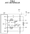
- the reference APP denotes a communication device, for example a cellular mobile telephone, equipped with an antenna ANT1 for establishing telephone communications.
- the device APP also comprises a conventional NFC system comprising a contactless CMP component of the NFC type, for example an NFC microcontroller.
- the CMP microcontroller conventionally has two contacts TX1, TX2 that can be used in reader mode and two other contacts RX1, RX2 that can be used in reader mode and in card mode.
- the CMP component can be equipped with an internal SWI switch making it possible to short-circuit terminals TX1 and TX2 for operation in card mode or not to short-circuit terminals TX1 and TX2 to authorize operation in mode reader.
- An ANT2 antenna for example an inductive winding, is usable for contactless communication with an external device.
- a first terminal B1 of this antenna ANT2 is connected to contacts TX1 and RX1 while the second terminal B2 of antenna ANT2 is connected to contacts TX2 and RX2.
- an external impedance matching circuit is connected between the antenna ANT2 and the component CMP.
- this impedance matching circuit may comprise an FL filter intended to filter electromagnetic interference (EMI filter).
- EMI filter electromagnetic interference
- This filter FL is conventionally an LC type filter here comprising a coil B11 connected in series, between contact TX1 and ground GND, with a capacitor C11.
- Filter FL also comprises a coil B12 connected in series, between contact TX2 and ground GND, with a capacitor C12.
- the inductance of coil B11 and coil B12 is equal to LEMI while the capacitive value of capacitors C11 and C12 is equal to CEMI.
- reference values are associated with a cutoff frequency of the EMI filter, referred to below as reference cutoff frequency (for example 20 MHz for a carrier frequency of 13.56 MHz).
- these reference values LEMI and CEMI are chosen to form a resonant circuit around the reference cut-off frequency f of the filter FL.
- CEMC 1 2 ⁇ 2 LEMI
- the impedance matching circuits also include capacitors C1, C2, CS1 and CS2.
- Capacitors C1 and C2 form a capacitive divider across contacts RX1 and RX2.
- the capacitors CS1 and CS2 are chosen to maximize the current in the antenna ANT2 so as to increase the amplitude of the electromagnetic field.
- the CMP component forms with the antenna ANT2 and the external impedance matching circuit a resonant circuit having a resonant frequency equal to the carrier frequency, for example 13.56 MHz in the case of a type A or type B communication protocol defined in the ISO/IEC 14443 standard.
- resonance frequencies contained in a range of +/- 15% around the carrier frequency can be considered as acceptable resonance frequencies.
- the real inductances and the real capacitive values of the various elements of this external impedance matching circuit may vary with respect to the theoretical values due in particular to the technological dispersion of coils and capacitors used.
- the antenna ANT2 can then no longer be tuned to an acceptable resonance frequency allowing correct communication of information.
- This frequency mismatch of the antenna can also be produced by the electromagnetic coupling with the antenna of the external device communicating with the CMP component.
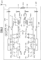
- the system comprising the antenna ANT2, the component CMP and the capacitive inductive network 1 connected between the antenna ANT2 and the component CMP further comprises processing means MTR configured to modify the impedance of the interference filtering means electromagnetic so as to control a frequency tuning of the antenna on an acceptable resonance frequency (frequency equal to or close to the carrier frequency for example), for example 13.56 MHz.
- the contacts TX1 and TX2 form a first and an output terminal of the component CMP for the transmission of data to the antenna ANT2 while the contacts RX1 and RX2 form two input terminals of the component for the reception of data from the ANT2 antenna.
- the electromagnetic interference filtering means 10 are this time configurable and capable of adopting different filtering configurations all having substantially the same reference cut-off frequency f, for example 20 MHz.
- the processing means MTR then comprise these configurable filtering means 10 and control means MCTL configured to select the filtering configuration for which the current flowing in the antenna ANT2 has the greatest value.
- first block BLC1 connected between the first output terminal (contact TX1) of the component and the first terminal B1 of the antenna ANT2.
- This first block BLC1 comprises a first main inductive element LP1 connected in parallel across the terminals of a first main capacitor CP1.
- a second block BLC2 is connected between the second output terminal (contact TX2) of the component CMP and the second terminal B2 of the antenna ANT2.
- This second block BLC2 comprises a second main inductive element LP2 connected in parallel across the terminals of a second main capacitor CP2.
- the main inductive elements LP1 and LP2 are advantageously identical.
- the main capacitors CP1 and CP2 are also advantageously identical.
- the two blocks BLC1 and BLC2 together form a capacitive inductive module.
- the configurable filtering means 10 also comprise a first additional capacitor connected in series between the first block BLC1 and ground GND and a second additional capacitor CA2 connected in series between the second block BLC2 and ground GND.
- the component CMP also comprises two auxiliary contacts A1 and A2 respectively forming a first and a second auxiliary terminals.
- the configurable filtering means 10 also comprise a first set of auxiliary capacitors CX1 1 -CX1 n respectively switchable via switches SW1 1 -SW1 n , for example MOS transistors.
- This first set of switchable auxiliary capacitors CX1 1 -CX1 n are connected in parallel between the first auxiliary terminal A1 and the first output terminal TX1 of the component.
- the filter means 10 also comprise a second set of auxiliary capacitors CX2 1 -CX2 n respectively switchable via switches SW2 1 -SW2 n , and connected in parallel between the second auxiliary terminal A2 and the second output terminal TX2 of the CMP component.
- This first set of switchable auxiliary capacitors and this second set of switchable auxiliary capacitors form a first set of auxiliary capacitive circuits.
- Two homologous auxiliary capacitors CX1 i and CX2 i have for example but not necessarily the same capacitive value.
- the configurable filtering means 10 also comprise a third set of auxiliary capacitors CX3 i -CX3 n respectively switchable via switches SW3 i -SW3 n , and connected in parallel between the first auxiliary terminal A1 and ground GND.
- the configurable filtering means 10 also comprise a fourth set of auxiliary capacitors CX4 1 -CX4 n respectively switchable via switches SW4 1 -SW4 n , and connected in parallel between the second auxiliary terminal A2 and ground GND.
- two homologous capacitors CX3 i , CX4 i have, for example, but not necessarily the same capacitive value.
- two homologous capacitors CX1 i and CX3 i may or may not have the same capacitive value.
- the two homologous capacitors CX2 i and CX4 i may also have or may not have the same capacitive value.
- This third set of switchable auxiliary capacitors and this fourth set of switchable auxiliary capacitors form a second set of auxiliary capacitive circuits.
- the component CMP therefore incorporates, in addition to the means suitable for processing the information received or transmitted, all the sets of auxiliary capacitors CX1 i , CX2 i , CX3 i , CX4 i . It is in fact preferable to place the auxiliary capacitors inside the CMP component so as not to oblige the user to add them outside the product. The circuit implementation cost will be reduced for the user.
- the control means MCTL also comprise a module MCD, based for example on logic circuits, intended to emitting a control signal SCTRL to control the various switches SW1-SW4.
- the filtering means 10 are formed by the first block BLC1 and the second block BLC2.
- control means MC2 control the switches so as, for example, to simultaneously close the four homologous switches SW1 i , SW2 i , SW3 i and SW4 i .
- auxiliary capacitor CX1 i is added in parallel with the first main capacitor CP1 and the auxiliary capacitor CX2 i is added in parallel with the second main capacitor CP2.
- auxiliary capacitor CX3 i is added in parallel with the first additional capacitor CA1 and the auxiliary capacitor CX4 i is added in parallel with the second additional capacitor CA2.
- CX1 i resp. CX2i
- CX3 i resp. CX4 i
- CX3 i resp. CX4 i
- each main inductive element LP1, LP2 is equal to LEMInew.
- each filtering configuration the capacitive value connected in parallel across the terminals of each main inductive element LP1 or LP2 is equal to CEMInew.
- this CEMInew capacitive value is different depending on the filtering configuration depending on the capacitor(s) actually connected to the terminals of each main element LP1 or LP2.
- this capacitive value CPEMInew differs for each filtering configuration depending on the capacitor(s) connected in parallel between each block BLC1, BLC2 and ground GND.
- Z LEMInew . ⁇ 1 ⁇ LEMInew . CEMInew . ⁇ 2 in which ⁇ designates the pulsation corresponding to the reference cut-off frequency f of the electromagnetic interference filter, for example 20 MHz.
- the value LEMInew and the capacitive values of the various main and auxiliary capacitors will be chosen so that this impedance Z is, in each filtering configuration, equal to the reference inductance LEMI.
- CPEMInew 1 2 ⁇ 2 LEMI where f denotes the reference cutoff frequency of the electromagnetic interference filter.
- the capacitive values of the various additional and auxiliary capacitors are chosen so as to satisfy this condition for each filtering configuration.
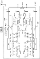
- the picture 3 illustrates by way of example another filtering configuration obtained by closing switches SW1 1 , SW3 1 , SW2 1 and SW4 1 . Therefore, in this filtering configuration, the additional capacitor CX1 i is connected in parallel to the terminals of the main capacitor CP1 and the auxiliary capacitor CX3 1 is connected in parallel to the terminals of the additional capacitor CA1.
- auxiliary capacitor CX2 1 is connected in parallel to the terminals of main capacitor CP2 and auxiliary capacitor CX4 1 to the terminals of additional capacitor CA2.
- control means MCTL will configure the filtering means 10 successively in their successive filtering configurations so as to determine the filtering configuration leading to the greatest value of current flowing in the antenna ANT2 .
- This filtering configuration will therefore correspond to that leading to the best tuning of the antenna ANT2 on a resonance frequency equal to or close to that determined theoretically, for example 13.56 MHz.
- control means may comprise for example one or here two DCT detectors connected between the terminals RX1 and RX2 and configured to detect the greatest voltage difference to the terminals of the ANT2 antenna.
- the choice of the filtering configuration can be made statically once the system has actually been produced with the various components welded.
Landscapes
- Engineering & Computer Science (AREA)
- Computer Networks & Wireless Communication (AREA)
- Signal Processing (AREA)
- Near-Field Transmission Systems (AREA)
- Filters And Equalizers (AREA)
- Transceivers (AREA)
- Power Engineering (AREA)
Claims (7)
- System, umfassend eine Antenne (ANT2), eine Komponente (CMP), die konfiguriert ist, um Informationen über die Antenne entsprechend einem kontaktlosen Kommunikationsprotokoll zu empfangen und/oder zu senden, und ein kapazitives, induktives Netzwerk (1), das zwischen der Antenne (ANT2) und der Komponente (CMP) angeschlossen ist, und Mittel zum Filtern von elektromagnetischen Interferenzen (10) beinhaltet, dadurch gekennzeichnet, dass es Verarbeitungsmittel (MTR) umfasst, die konfiguriert sind, um die Impedanz der Mittel zum Filtern von elektromagnetischen Interferenzen (10) zu ändern, um eine Frequenzübereinstimmung der Antenne, in der die Filtermittel (10) konfigurierbar und imstande sind, unterschiedliche Filterkonfigurationen einzunehmen, die allesamt eine im Wesentlichen gleiche Referenz-Grenzfrequenz (f) aufweisen, zu kontrollieren, und die Verarbeitungsmittel (MTR) die konfigurierbaren Filtermittel (10) und Kontrollmittel (MCTL) beinhalten, die konfiguriert sind, um die Filterkonfiguration auszuwählen, bei der der Strom, der in der Antenne (ANT2) fließt, den größten Wert aufweist, und wobei die Filtermittel (10) eine Referenz-Induktivität (LEMI) und einen kapazitiven Referenzwert (CEMI) besitzen, die der Referenz-Grenzfrequenz (f) zugewiesen sind, die Filtermittel (10) einen konfigurierbaren kapazitiven induktiven Kreis beinhalten, der zwischen der Komponente (CMP) und den Klemmen der Antenne (ANT2) angeschlossen ist, und einen konfigurierbaren kapazitiven Kreis, der zwischen dem kapazitiven induktiven Kreis und einem Cold Spot (GND) angeschlossen ist, der konfigurierbare kapazitive induktive Kreis ein kapazitives induktives Modul (BLC1, BLC2) beinhaltet, das durch einen ersten Satz an umschaltbaren kapazitiven Hilfskreisen (CX1i, CX2i) konfigurierbar ist, und der konfigurierbare kapazitive Kreis ein kapazitives Modul (CA1, CA2) beinhaltet, das durch einen zweiten Satz an umschaltbaren kapazitiven Hilfskreisen (CX3i, CX4i) konfigurierbar ist, und in jeder Filterkonfiguration die Impedanz des kapazitiven induktiven Kreises bei der Grenzfrequenz gleich der Referenz-Induktivität (LEMI) ist, und die Impedanz des kapazitiven Kreises bei der Grenzfrequenz gleich dem kapazitiven Referenzwert (CEMI) ist.
- System nach Anspruch 1, wobei in der einen der Filterkonfigurationen kein kapazitiver Hilfskreis an die Klemmen des kapazitiven induktiven Moduls (BLC1, BLC2) angeschlossen ist, und kein kapazitiver Hilfskreis an die Klemmen des kapazitiven Moduls (CA1, CA2) angeschlossen ist, und in jeder anderen Filterkonfiguration ein kapazitiver Hilfskreis (CX1i, CX2i) des ersten Satzes an die Klemmen des kapazitiven induktiven Moduls angeschlossen ist, und ein kapazitiver Hilfskreis (CX3i, CX4i) des zweiten Satzes an die Klemmen des kapazitiven Moduls angeschlossen ist.
- System nach Anspruch 1 oder 2, wobei sich der erste und zweite Satz an umschaltbaren kapazitiven Hilfskreisen (CX1i, CX2i, CX3i, CX4i) im Inneren der Komponente (CMP) befinden.
- System nach Anspruch 3, wobei die Komponente (CMP) eine erste Ausgangsklemme (TX1) und eine zweite Ausgangsklemme (TX2) zum Senden von Daten zur Antenne, und eine erste und eine zweite Hilfsklemme (A1, A2) beinhaltet,das kapazitive induktive Modul einen ersten Block (BLC1) umfasst, der zwischen der ersten Ausgangsklemme (TX1) und einer ersten Klemme (B1) der Antenne angeschlossen ist, und ein erstes induktives Hauptelement (LP1) beinhaltet, das parallel an die Klemmen eines ersten Hauptkondensators (CP1) angeschlossen ist, und einen zweiten Block (BLC2), der zwischen der zweiten Ausgangsklemme (TX2) und einer zweiten Klemme (B2) der Antenne angeschlossen ist, und ein zweites induktives Hauptelement (LP2) beinhaltet, das parallel an die Klemmen eines zweiten Hauptkondensators (CP2) angeschlossen ist,das kapazitive Modul einen ersten zusätzlichen Kondensator (CA1) umfasst, der in Reihe zwischen dem ersten Block (BLC1) und dem Cold Spot (GND) angeschlossen ist, und einen zweiten zusätzlichen Kondensator (CA2), der in Reihe zwischen dem zweiten Block (BLC2) und dem Cold Spot (GND) angeschlossen ist,wobei der erste Satz an kapazitiven Hilfskreisen eine erste Einheit an umschaltbaren Hilfskondensatoren (CX1i) umfasst, die parallel zwischen der ersten Hilfsklemme (A1) und der ersten Ausgangsklemme (TX1) angeschlossen sind, und eine zweite Einheit an umschaltbaren Hilfskondensatoren (CX2i), die parallel zwischen der zweiten Hilfsklemme (A2) und der zweiten Ausgangsklemme (TX2) angeschlossen sind,und der zweite Satz an kapazitiven Hilfskreisen eine dritte Einheit an umschaltbaren Hilfskondensatoren (CX3i) umfasst, die parallel zwischen der ersten Hilfsklemme (A1) und dem Cold Spot (GND) angeschlossen sind, und eine vierte Einheit an umschaltbaren Hilfskondensatoren (CX4i), die parallel zwischen der zweiten Hilfsklemme (A2) und dem Cold Spot (GND) angeschlossen sind.
- System nach einem der vorstehenden Ansprüche, wobei die Komponente (CMP) eine erste und eine zweite Eingangsklemme (RX1, RX2) umfasst, die an die beiden Klemmen der Antenne zum Empfangen von Daten angeschlossen sind, die von der Antenne stammen, und die Kontrollmittel mindestens einen Detektor (DCT) umfassen, der konfiguriert ist, um die größte Spannung an den Klemmen der Antenne zu detektieren.
- System nach einem der vorstehenden Ansprüche, wobei die Komponente (CMP) imstande ist, im Lesermodus oder im Kartenmodus betrieben zu werden.
- Drahtlose Kommunikationseinrichtung, umfassend ein System nach einem der vorstehenden Ansprüche.
Applications Claiming Priority (1)
| Application Number | Priority Date | Filing Date | Title |
|---|---|---|---|
| FR1554987A FR3037201B1 (fr) | 2015-06-02 | 2015-06-02 | Procede de controle de l'accord sur une frequence de communication d'une antenne connectee a un composant adapte a une communication sans contact, et systeme correspondant |
Publications (2)
| Publication Number | Publication Date |
|---|---|
| EP3101816A1 EP3101816A1 (de) | 2016-12-07 |
| EP3101816B1 true EP3101816B1 (de) | 2022-11-30 |
Family
ID=54260865
Family Applications (1)
| Application Number | Title | Priority Date | Filing Date |
|---|---|---|---|
| EP15190532.0A Active EP3101816B1 (de) | 2015-06-02 | 2015-10-20 | System und vorrichtung zur steuerung der abstimmung auf eine kommunikationsfrequenz einer antenne, die mit einer komponente verbunden ist, die für eine kontaktlose kommunikation ausgelegt ist. |
Country Status (4)
| Country | Link |
|---|---|
| US (2) | US9853677B2 (de) |
| EP (1) | EP3101816B1 (de) |
| CN (3) | CN110061750B (de) |
| FR (1) | FR3037201B1 (de) |
Families Citing this family (7)
| Publication number | Priority date | Publication date | Assignee | Title |
|---|---|---|---|---|
| SG10201706957QA (en) | 2013-03-01 | 2017-09-28 | Procter & Gamble | Insect trap device and method of using |
| CN105848478B (zh) | 2013-11-27 | 2020-10-16 | 宝洁公司 | 昆虫诱捕装置及使用方法 |
| CN112616791B (zh) | 2014-04-26 | 2023-06-16 | 宝洁公司 | 昆虫诱捕装置及使用方法 |
| EP3270689B1 (de) | 2015-01-12 | 2022-04-13 | The Procter & Gamble Company | Insektenfalle |
| FR3037201B1 (fr) * | 2015-06-02 | 2018-07-13 | Stmicroelectronics (Rousset) Sas | Procede de controle de l'accord sur une frequence de communication d'une antenne connectee a un composant adapte a une communication sans contact, et systeme correspondant |
| FR3096548B1 (fr) * | 2019-05-21 | 2021-06-25 | Commissariat Energie Atomique | Correction d'une valeur d'un composant passif |
| FR3098067B1 (fr) * | 2019-06-25 | 2022-12-23 | St Microelectronics Rousset | Détection de dispositifs NFC |
Citations (1)
| Publication number | Priority date | Publication date | Assignee | Title |
|---|---|---|---|---|
| US20140106668A1 (en) * | 2012-10-11 | 2014-04-17 | Qualcomm Incorporated | Circuit tuning for device detection in near-field communications |
Family Cites Families (11)
| Publication number | Priority date | Publication date | Assignee | Title |
|---|---|---|---|---|
| US7539465B2 (en) * | 2006-10-16 | 2009-05-26 | Assa Abloy Ab | Tuning an RFID reader with electronic switches |
| US8559890B2 (en) * | 2007-11-19 | 2013-10-15 | Nxp B.V. | Transceiving circuit for contactless communication |
| FR2971378B1 (fr) * | 2011-02-04 | 2013-02-22 | St Microelectronics Rousset | Procede de connexion sur une seule antenne d'un ou de plusieurs composants sans contact, et systeme correspondant |
| US9879546B2 (en) * | 2012-06-21 | 2018-01-30 | United Technologies Corporation | Airfoil cooling circuits |
| US9292721B2 (en) * | 2013-03-01 | 2016-03-22 | Texas Instruments Incorporated | NFC receiver architecture with improved power sensitivity |
| EP2824846A1 (de) | 2013-07-08 | 2015-01-14 | ST-Ericsson SA | Nahfeldkommunikationsfähige Vorrichtung mit verbesserter elektromagnetischer Kompatibilität und Verfahren zur Lastmodulierung bei der Nahfeldkommunikation |
| EP2830228B1 (de) * | 2013-07-23 | 2018-01-10 | Nxp B.V. | HF-Vorrichtung und Verfahren mit verbesserter aktiver Belastungsmodulationskapazität |
| CN110557174A (zh) * | 2013-09-04 | 2019-12-10 | 联发科技(新加坡)私人有限公司 | 包络提取装置,信号解码装置和短距离非接触通信装置及相关方法 |
| KR102155199B1 (ko) * | 2013-12-23 | 2020-09-11 | 삼성전자주식회사 | Nfc 장치의 매칭 회로, nfc 장치 및 전자 시스템 |
| CN104580605B (zh) * | 2015-01-30 | 2017-11-14 | 昆山睿翔讯通通信技术有限公司 | 基于自适应匹配电路的nfc手机电路系统 |
| FR3037201B1 (fr) | 2015-06-02 | 2018-07-13 | Stmicroelectronics (Rousset) Sas | Procede de controle de l'accord sur une frequence de communication d'une antenne connectee a un composant adapte a une communication sans contact, et systeme correspondant |
-
2015
- 2015-06-02 FR FR1554987A patent/FR3037201B1/fr not_active Expired - Fee Related
- 2015-10-20 EP EP15190532.0A patent/EP3101816B1/de active Active
- 2015-11-26 CN CN201910132934.3A patent/CN110061750B/zh active Active
- 2015-11-26 CN CN201510844731.9A patent/CN106230487B/zh active Active
- 2015-11-26 CN CN201520963457.2U patent/CN205377868U/zh not_active Expired - Lifetime
- 2015-12-18 US US14/974,146 patent/US9853677B2/en active Active
-
2017
- 2017-10-09 US US15/728,150 patent/US10419058B2/en active Active
Patent Citations (1)
| Publication number | Priority date | Publication date | Assignee | Title |
|---|---|---|---|---|
| US20140106668A1 (en) * | 2012-10-11 | 2014-04-17 | Qualcomm Incorporated | Circuit tuning for device detection in near-field communications |
Also Published As
| Publication number | Publication date |
|---|---|
| US10419058B2 (en) | 2019-09-17 |
| CN110061750B (zh) | 2021-04-20 |
| CN205377868U (zh) | 2016-07-06 |
| CN106230487B (zh) | 2019-03-19 |
| US20180034497A1 (en) | 2018-02-01 |
| FR3037201A1 (fr) | 2016-12-09 |
| EP3101816A1 (de) | 2016-12-07 |
| CN106230487A (zh) | 2016-12-14 |
| FR3037201B1 (fr) | 2018-07-13 |
| US9853677B2 (en) | 2017-12-26 |
| US20160359519A1 (en) | 2016-12-08 |
| CN110061750A (zh) | 2019-07-26 |
Similar Documents
| Publication | Publication Date | Title |
|---|---|---|
| EP3101816B1 (de) | System und vorrichtung zur steuerung der abstimmung auf eine kommunikationsfrequenz einer antenne, die mit einer komponente verbunden ist, die für eine kontaktlose kommunikation ausgelegt ist. | |
| EP1473833B1 (de) | Integrierte zwei-band Induktivität und Anwendungen | |
| EP2690796B1 (de) | Steuerverfahren zur Anpassung einer Antenne, die mit einem NFC-Komponent verbunden ist, und das entsprechenden NFC-Komponent | |
| EP2485396B1 (de) | Verfahren zum Anschluss einer oder mehreren kontaktlosen Komponenten auf einer einzigen Antenne, und entsprechendes System | |
| EP3561730B1 (de) | Regulierungsverfahren der phase des signals, das von einem objekt abgegeben wird, das durch aktive modulierung der ladung kontaktlos mit einem lesegerät kommunizieren kann, und entsprechendes objekt | |
| JP2002540664A (ja) | ハイパスフィルタ | |
| EP1172929A1 (de) | Rauscharme Verstärkungsanordnung insbesondere für ein zellulares Mobiltelefon | |
| EP2204877A1 (de) | Regelung eines Baluns | |
| EP1099188A1 (de) | Verbessertes lesegerät für kontaktlose etiketten | |
| FR2796782A1 (fr) | Dimensionnement d'un systeme a transpondeur electromagnetique pour un fonctionnement dedie en couplage lointain | |
| EP3048743B1 (de) | Verfahren zur steuerung der kontaktlosen kommunikation und der kontaktlosen ladung innerhalb eines systems, und entsprechendes system | |
| EP3035439A1 (de) | Antenne für elektronische vorrichtung | |
| FR2578131A1 (fr) | Piege de frequence image suivant les variations d'accord | |
| EP3427189B1 (de) | Fingergesteuerte kontaktlose chipkarte | |
| FR2887665A1 (fr) | Entite electronique a antenne magnetique | |
| EP2652835A1 (de) | Aktives bandstopp-filter | |
| EP0792027A1 (de) | Mehrband-Funkgerät | |
| FR2982686A1 (fr) | Protection d'un terminal d'emission-reception radio-frequence contre des perturbations electromagnetiques | |
| WO2002001718A1 (fr) | Dispositif de filtrage passe bande de frequence auto adaptatif dans un emetteur/recepteur de signaux hyperfrequences | |
| FR3105506A1 (fr) | Configuration d'un terminal mobile NFC | |
| FR3105697A1 (fr) | Configuration d'un terminal mobile NFC | |
| FR2622054A1 (fr) | Cavite a accord commutable pour filtre passe-bande, notamment pour duplexeur, et emetteur-recepteur pour radiotelephonie comprenant une telle cavite | |
| FR2784524A1 (fr) | Antenne perfectionnee, notamment pour un lecteur de badge sans contact | |
| FR3073995A1 (fr) | Systeme d'au moins deux unites emettrices et/ou receptrices reliees a une antenne commune | |
| EP4668593A1 (de) | Elektronische vorrichtung mit drahtloser verbindung |
Legal Events
| Date | Code | Title | Description |
|---|---|---|---|
| PUAI | Public reference made under article 153(3) epc to a published international application that has entered the european phase |
Free format text: ORIGINAL CODE: 0009012 |
|
| STAA | Information on the status of an ep patent application or granted ep patent |
Free format text: STATUS: REQUEST FOR EXAMINATION WAS MADE |
|
| 17P | Request for examination filed |
Effective date: 20151020 |
|
| AK | Designated contracting states |
Kind code of ref document: A1 Designated state(s): AL AT BE BG CH CY CZ DE DK EE ES FI FR GB GR HR HU IE IS IT LI LT LU LV MC MK MT NL NO PL PT RO RS SE SI SK SM TR |
|
| AX | Request for extension of the european patent |
Extension state: BA ME |
|
| STAA | Information on the status of an ep patent application or granted ep patent |
Free format text: STATUS: EXAMINATION IS IN PROGRESS |
|
| 17Q | First examination report despatched |
Effective date: 20200723 |
|
| GRAP | Despatch of communication of intention to grant a patent |
Free format text: ORIGINAL CODE: EPIDOSNIGR1 |
|
| STAA | Information on the status of an ep patent application or granted ep patent |
Free format text: STATUS: GRANT OF PATENT IS INTENDED |
|
| INTG | Intention to grant announced |
Effective date: 20220819 |
|
| GRAS | Grant fee paid |
Free format text: ORIGINAL CODE: EPIDOSNIGR3 |
|
| GRAA | (expected) grant |
Free format text: ORIGINAL CODE: 0009210 |
|
| STAA | Information on the status of an ep patent application or granted ep patent |
Free format text: STATUS: THE PATENT HAS BEEN GRANTED |
|
| AK | Designated contracting states |
Kind code of ref document: B1 Designated state(s): AL AT BE BG CH CY CZ DE DK EE ES FI FR GB GR HR HU IE IS IT LI LT LU LV MC MK MT NL NO PL PT RO RS SE SI SK SM TR |
|
| REG | Reference to a national code |
Ref country code: CH Ref legal event code: EP Ref country code: GB Ref legal event code: FG4D Free format text: NOT ENGLISH |
|
| REG | Reference to a national code |
Ref country code: AT Ref legal event code: REF Ref document number: 1535492 Country of ref document: AT Kind code of ref document: T Effective date: 20221215 Ref country code: DE Ref legal event code: R096 Ref document number: 602015081766 Country of ref document: DE |
|
| REG | Reference to a national code |
Ref country code: IE Ref legal event code: FG4D Free format text: LANGUAGE OF EP DOCUMENT: FRENCH |
|
| REG | Reference to a national code |
Ref country code: LT Ref legal event code: MG9D |
|
| REG | Reference to a national code |
Ref country code: NL Ref legal event code: MP Effective date: 20221130 |
|
| PG25 | Lapsed in a contracting state [announced via postgrant information from national office to epo] |
Ref country code: SE Free format text: LAPSE BECAUSE OF FAILURE TO SUBMIT A TRANSLATION OF THE DESCRIPTION OR TO PAY THE FEE WITHIN THE PRESCRIBED TIME-LIMIT Effective date: 20221130 Ref country code: PT Free format text: LAPSE BECAUSE OF FAILURE TO SUBMIT A TRANSLATION OF THE DESCRIPTION OR TO PAY THE FEE WITHIN THE PRESCRIBED TIME-LIMIT Effective date: 20230331 Ref country code: NO Free format text: LAPSE BECAUSE OF FAILURE TO SUBMIT A TRANSLATION OF THE DESCRIPTION OR TO PAY THE FEE WITHIN THE PRESCRIBED TIME-LIMIT Effective date: 20230228 Ref country code: LT Free format text: LAPSE BECAUSE OF FAILURE TO SUBMIT A TRANSLATION OF THE DESCRIPTION OR TO PAY THE FEE WITHIN THE PRESCRIBED TIME-LIMIT Effective date: 20221130 Ref country code: FI Free format text: LAPSE BECAUSE OF FAILURE TO SUBMIT A TRANSLATION OF THE DESCRIPTION OR TO PAY THE FEE WITHIN THE PRESCRIBED TIME-LIMIT Effective date: 20221130 Ref country code: ES Free format text: LAPSE BECAUSE OF FAILURE TO SUBMIT A TRANSLATION OF THE DESCRIPTION OR TO PAY THE FEE WITHIN THE PRESCRIBED TIME-LIMIT Effective date: 20221130 |
|
| REG | Reference to a national code |
Ref country code: AT Ref legal event code: MK05 Ref document number: 1535492 Country of ref document: AT Kind code of ref document: T Effective date: 20221130 |
|
| PG25 | Lapsed in a contracting state [announced via postgrant information from national office to epo] |
Ref country code: RS Free format text: LAPSE BECAUSE OF FAILURE TO SUBMIT A TRANSLATION OF THE DESCRIPTION OR TO PAY THE FEE WITHIN THE PRESCRIBED TIME-LIMIT Effective date: 20221130 Ref country code: PL Free format text: LAPSE BECAUSE OF FAILURE TO SUBMIT A TRANSLATION OF THE DESCRIPTION OR TO PAY THE FEE WITHIN THE PRESCRIBED TIME-LIMIT Effective date: 20221130 Ref country code: LV Free format text: LAPSE BECAUSE OF FAILURE TO SUBMIT A TRANSLATION OF THE DESCRIPTION OR TO PAY THE FEE WITHIN THE PRESCRIBED TIME-LIMIT Effective date: 20221130 Ref country code: IS Free format text: LAPSE BECAUSE OF FAILURE TO SUBMIT A TRANSLATION OF THE DESCRIPTION OR TO PAY THE FEE WITHIN THE PRESCRIBED TIME-LIMIT Effective date: 20230330 Ref country code: HR Free format text: LAPSE BECAUSE OF FAILURE TO SUBMIT A TRANSLATION OF THE DESCRIPTION OR TO PAY THE FEE WITHIN THE PRESCRIBED TIME-LIMIT Effective date: 20221130 Ref country code: GR Free format text: LAPSE BECAUSE OF FAILURE TO SUBMIT A TRANSLATION OF THE DESCRIPTION OR TO PAY THE FEE WITHIN THE PRESCRIBED TIME-LIMIT Effective date: 20230301 |
|
| PG25 | Lapsed in a contracting state [announced via postgrant information from national office to epo] |
Ref country code: NL Free format text: LAPSE BECAUSE OF FAILURE TO SUBMIT A TRANSLATION OF THE DESCRIPTION OR TO PAY THE FEE WITHIN THE PRESCRIBED TIME-LIMIT Effective date: 20221130 |
|
| PG25 | Lapsed in a contracting state [announced via postgrant information from national office to epo] |
Ref country code: SM Free format text: LAPSE BECAUSE OF FAILURE TO SUBMIT A TRANSLATION OF THE DESCRIPTION OR TO PAY THE FEE WITHIN THE PRESCRIBED TIME-LIMIT Effective date: 20221130 Ref country code: RO Free format text: LAPSE BECAUSE OF FAILURE TO SUBMIT A TRANSLATION OF THE DESCRIPTION OR TO PAY THE FEE WITHIN THE PRESCRIBED TIME-LIMIT Effective date: 20221130 Ref country code: EE Free format text: LAPSE BECAUSE OF FAILURE TO SUBMIT A TRANSLATION OF THE DESCRIPTION OR TO PAY THE FEE WITHIN THE PRESCRIBED TIME-LIMIT Effective date: 20221130 Ref country code: DK Free format text: LAPSE BECAUSE OF FAILURE TO SUBMIT A TRANSLATION OF THE DESCRIPTION OR TO PAY THE FEE WITHIN THE PRESCRIBED TIME-LIMIT Effective date: 20221130 Ref country code: CZ Free format text: LAPSE BECAUSE OF FAILURE TO SUBMIT A TRANSLATION OF THE DESCRIPTION OR TO PAY THE FEE WITHIN THE PRESCRIBED TIME-LIMIT Effective date: 20221130 Ref country code: AT Free format text: LAPSE BECAUSE OF FAILURE TO SUBMIT A TRANSLATION OF THE DESCRIPTION OR TO PAY THE FEE WITHIN THE PRESCRIBED TIME-LIMIT Effective date: 20221130 |
|
| PG25 | Lapsed in a contracting state [announced via postgrant information from national office to epo] |
Ref country code: SK Free format text: LAPSE BECAUSE OF FAILURE TO SUBMIT A TRANSLATION OF THE DESCRIPTION OR TO PAY THE FEE WITHIN THE PRESCRIBED TIME-LIMIT Effective date: 20221130 Ref country code: AL Free format text: LAPSE BECAUSE OF FAILURE TO SUBMIT A TRANSLATION OF THE DESCRIPTION OR TO PAY THE FEE WITHIN THE PRESCRIBED TIME-LIMIT Effective date: 20221130 |
|
| REG | Reference to a national code |
Ref country code: DE Ref legal event code: R097 Ref document number: 602015081766 Country of ref document: DE |
|
| PLBE | No opposition filed within time limit |
Free format text: ORIGINAL CODE: 0009261 |
|
| STAA | Information on the status of an ep patent application or granted ep patent |
Free format text: STATUS: NO OPPOSITION FILED WITHIN TIME LIMIT |
|
| 26N | No opposition filed |
Effective date: 20230831 |
|
| PG25 | Lapsed in a contracting state [announced via postgrant information from national office to epo] |
Ref country code: SI Free format text: LAPSE BECAUSE OF FAILURE TO SUBMIT A TRANSLATION OF THE DESCRIPTION OR TO PAY THE FEE WITHIN THE PRESCRIBED TIME-LIMIT Effective date: 20221130 |
|
| PG25 | Lapsed in a contracting state [announced via postgrant information from national office to epo] |
Ref country code: IT Free format text: LAPSE BECAUSE OF FAILURE TO SUBMIT A TRANSLATION OF THE DESCRIPTION OR TO PAY THE FEE WITHIN THE PRESCRIBED TIME-LIMIT Effective date: 20221130 Ref country code: MC Free format text: LAPSE BECAUSE OF FAILURE TO SUBMIT A TRANSLATION OF THE DESCRIPTION OR TO PAY THE FEE WITHIN THE PRESCRIBED TIME-LIMIT Effective date: 20221130 |
|
| REG | Reference to a national code |
Ref country code: CH Ref legal event code: PL |
|
| REG | Reference to a national code |
Ref country code: BE Ref legal event code: MM Effective date: 20231031 |
|
| PG25 | Lapsed in a contracting state [announced via postgrant information from national office to epo] |
Ref country code: LU Free format text: LAPSE BECAUSE OF NON-PAYMENT OF DUE FEES Effective date: 20231020 |
|
| GBPC | Gb: european patent ceased through non-payment of renewal fee |
Effective date: 20231020 |
|
| PG25 | Lapsed in a contracting state [announced via postgrant information from national office to epo] |
Ref country code: LU Free format text: LAPSE BECAUSE OF NON-PAYMENT OF DUE FEES Effective date: 20231020 |
|
| PG25 | Lapsed in a contracting state [announced via postgrant information from national office to epo] |
Ref country code: GB Free format text: LAPSE BECAUSE OF NON-PAYMENT OF DUE FEES Effective date: 20231020 |
|
| PG25 | Lapsed in a contracting state [announced via postgrant information from national office to epo] |
Ref country code: CH Free format text: LAPSE BECAUSE OF NON-PAYMENT OF DUE FEES Effective date: 20231031 |
|
| PG25 | Lapsed in a contracting state [announced via postgrant information from national office to epo] |
Ref country code: GB Free format text: LAPSE BECAUSE OF NON-PAYMENT OF DUE FEES Effective date: 20231020 Ref country code: FR Free format text: LAPSE BECAUSE OF NON-PAYMENT OF DUE FEES Effective date: 20231031 Ref country code: CH Free format text: LAPSE BECAUSE OF NON-PAYMENT OF DUE FEES Effective date: 20231031 |
|
| PG25 | Lapsed in a contracting state [announced via postgrant information from national office to epo] |
Ref country code: BE Free format text: LAPSE BECAUSE OF NON-PAYMENT OF DUE FEES Effective date: 20231031 |
|
| PG25 | Lapsed in a contracting state [announced via postgrant information from national office to epo] |
Ref country code: IE Free format text: LAPSE BECAUSE OF NON-PAYMENT OF DUE FEES Effective date: 20231020 |
|
| PG25 | Lapsed in a contracting state [announced via postgrant information from national office to epo] |
Ref country code: IE Free format text: LAPSE BECAUSE OF NON-PAYMENT OF DUE FEES Effective date: 20231020 |
|
| PG25 | Lapsed in a contracting state [announced via postgrant information from national office to epo] |
Ref country code: BG Free format text: LAPSE BECAUSE OF FAILURE TO SUBMIT A TRANSLATION OF THE DESCRIPTION OR TO PAY THE FEE WITHIN THE PRESCRIBED TIME-LIMIT Effective date: 20221130 |
|
| PG25 | Lapsed in a contracting state [announced via postgrant information from national office to epo] |
Ref country code: BG Free format text: LAPSE BECAUSE OF FAILURE TO SUBMIT A TRANSLATION OF THE DESCRIPTION OR TO PAY THE FEE WITHIN THE PRESCRIBED TIME-LIMIT Effective date: 20221130 |
|
| PG25 | Lapsed in a contracting state [announced via postgrant information from national office to epo] |
Ref country code: CY Free format text: LAPSE BECAUSE OF FAILURE TO SUBMIT A TRANSLATION OF THE DESCRIPTION OR TO PAY THE FEE WITHIN THE PRESCRIBED TIME-LIMIT; INVALID AB INITIO Effective date: 20151020 |
|
| PG25 | Lapsed in a contracting state [announced via postgrant information from national office to epo] |
Ref country code: HU Free format text: LAPSE BECAUSE OF FAILURE TO SUBMIT A TRANSLATION OF THE DESCRIPTION OR TO PAY THE FEE WITHIN THE PRESCRIBED TIME-LIMIT; INVALID AB INITIO Effective date: 20151020 |
|
| PG25 | Lapsed in a contracting state [announced via postgrant information from national office to epo] |
Ref country code: TR Free format text: LAPSE BECAUSE OF FAILURE TO SUBMIT A TRANSLATION OF THE DESCRIPTION OR TO PAY THE FEE WITHIN THE PRESCRIBED TIME-LIMIT Effective date: 20221130 |
|
| PGFP | Annual fee paid to national office [announced via postgrant information from national office to epo] |
Ref country code: DE Payment date: 20250923 Year of fee payment: 11 |