EP3059761A2 - Oberflächenmontierbares bauelement mit einem oder mehreren chips zwischen zwei leiterplatten und verfahren zur herstellung davon - Google Patents
Oberflächenmontierbares bauelement mit einem oder mehreren chips zwischen zwei leiterplatten und verfahren zur herstellung davon Download PDFInfo
- Publication number
- EP3059761A2 EP3059761A2 EP16155607.1A EP16155607A EP3059761A2 EP 3059761 A2 EP3059761 A2 EP 3059761A2 EP 16155607 A EP16155607 A EP 16155607A EP 3059761 A2 EP3059761 A2 EP 3059761A2
- Authority
- EP
- European Patent Office
- Prior art keywords
- chip
- circuit board
- electrode
- die
- substrate
- Prior art date
- Legal status (The legal status is an assumption and is not a legal conclusion. Google has not performed a legal analysis and makes no representation as to the accuracy of the status listed.)
- Withdrawn
Links
Images


Classifications
-
- H—ELECTRICITY
- H10—SEMICONDUCTOR DEVICES; ELECTRIC SOLID-STATE DEVICES NOT OTHERWISE PROVIDED FOR
- H10W—GENERIC PACKAGES, INTERCONNECTIONS, CONNECTORS OR OTHER CONSTRUCTIONAL DETAILS OF DEVICES COVERED BY CLASS H10
- H10W90/00—Package configurations
-
- H—ELECTRICITY
- H10—SEMICONDUCTOR DEVICES; ELECTRIC SOLID-STATE DEVICES NOT OTHERWISE PROVIDED FOR
- H10W—GENERIC PACKAGES, INTERCONNECTIONS, CONNECTORS OR OTHER CONSTRUCTIONAL DETAILS OF DEVICES COVERED BY CLASS H10
- H10W70/00—Package substrates; Interposers; Redistribution layers [RDL]
- H10W70/60—Insulating or insulated package substrates; Interposers; Redistribution layers
- H10W70/611—Insulating or insulated package substrates; Interposers; Redistribution layers for connecting multiple chips together
-
- H—ELECTRICITY
- H10—SEMICONDUCTOR DEVICES; ELECTRIC SOLID-STATE DEVICES NOT OTHERWISE PROVIDED FOR
- H10W—GENERIC PACKAGES, INTERCONNECTIONS, CONNECTORS OR OTHER CONSTRUCTIONAL DETAILS OF DEVICES COVERED BY CLASS H10
- H10W70/00—Package substrates; Interposers; Redistribution layers [RDL]
- H10W70/60—Insulating or insulated package substrates; Interposers; Redistribution layers
- H10W70/611—Insulating or insulated package substrates; Interposers; Redistribution layers for connecting multiple chips together
- H10W70/614—Insulating or insulated package substrates; Interposers; Redistribution layers for connecting multiple chips together the multiple chips being integrally enclosed
-
- H—ELECTRICITY
- H10—SEMICONDUCTOR DEVICES; ELECTRIC SOLID-STATE DEVICES NOT OTHERWISE PROVIDED FOR
- H10W—GENERIC PACKAGES, INTERCONNECTIONS, CONNECTORS OR OTHER CONSTRUCTIONAL DETAILS OF DEVICES COVERED BY CLASS H10
- H10W70/00—Package substrates; Interposers; Redistribution layers [RDL]
- H10W70/60—Insulating or insulated package substrates; Interposers; Redistribution layers
- H10W70/62—Insulating or insulated package substrates; Interposers; Redistribution layers characterised by their interconnections
- H10W70/65—Shapes or dispositions of interconnections
- H10W70/657—Shapes or dispositions of interconnections on sidewalls or bottom surfaces of the package substrates, interposers or redistribution layers
-
- H—ELECTRICITY
- H10—SEMICONDUCTOR DEVICES; ELECTRIC SOLID-STATE DEVICES NOT OTHERWISE PROVIDED FOR
- H10W—GENERIC PACKAGES, INTERCONNECTIONS, CONNECTORS OR OTHER CONSTRUCTIONAL DETAILS OF DEVICES COVERED BY CLASS H10
- H10W74/00—Encapsulations, e.g. protective coatings
- H10W74/10—Encapsulations, e.g. protective coatings characterised by their shape or disposition
- H10W74/111—Encapsulations, e.g. protective coatings characterised by their shape or disposition the semiconductor body being completely enclosed
- H10W74/114—Encapsulations, e.g. protective coatings characterised by their shape or disposition the semiconductor body being completely enclosed by a substrate and the encapsulations
-
- H—ELECTRICITY
- H10—SEMICONDUCTOR DEVICES; ELECTRIC SOLID-STATE DEVICES NOT OTHERWISE PROVIDED FOR
- H10W—GENERIC PACKAGES, INTERCONNECTIONS, CONNECTORS OR OTHER CONSTRUCTIONAL DETAILS OF DEVICES COVERED BY CLASS H10
- H10W90/00—Package configurations
- H10W90/401—Package configurations characterised by multiple insulating or insulated package substrates, interposers or RDLs
-
- H—ELECTRICITY
- H10—SEMICONDUCTOR DEVICES; ELECTRIC SOLID-STATE DEVICES NOT OTHERWISE PROVIDED FOR
- H10W—GENERIC PACKAGES, INTERCONNECTIONS, CONNECTORS OR OTHER CONSTRUCTIONAL DETAILS OF DEVICES COVERED BY CLASS H10
- H10W72/00—Interconnections or connectors in packages
- H10W72/01—Manufacture or treatment
- H10W72/013—Manufacture or treatment of die-attach connectors
- H10W72/01321—Manufacture or treatment of die-attach connectors using local deposition
- H10W72/01323—Manufacture or treatment of die-attach connectors using local deposition in liquid form, e.g. by dispensing droplets or by screen printing
-
- H—ELECTRICITY
- H10—SEMICONDUCTOR DEVICES; ELECTRIC SOLID-STATE DEVICES NOT OTHERWISE PROVIDED FOR
- H10W—GENERIC PACKAGES, INTERCONNECTIONS, CONNECTORS OR OTHER CONSTRUCTIONAL DETAILS OF DEVICES COVERED BY CLASS H10
- H10W72/00—Interconnections or connectors in packages
- H10W72/01—Manufacture or treatment
- H10W72/0198—Manufacture or treatment batch processes
-
- H—ELECTRICITY
- H10—SEMICONDUCTOR DEVICES; ELECTRIC SOLID-STATE DEVICES NOT OTHERWISE PROVIDED FOR
- H10W—GENERIC PACKAGES, INTERCONNECTIONS, CONNECTORS OR OTHER CONSTRUCTIONAL DETAILS OF DEVICES COVERED BY CLASS H10
- H10W72/00—Interconnections or connectors in packages
- H10W72/071—Connecting or disconnecting
- H10W72/073—Connecting or disconnecting of die-attach connectors
-
- H—ELECTRICITY
- H10—SEMICONDUCTOR DEVICES; ELECTRIC SOLID-STATE DEVICES NOT OTHERWISE PROVIDED FOR
- H10W—GENERIC PACKAGES, INTERCONNECTIONS, CONNECTORS OR OTHER CONSTRUCTIONAL DETAILS OF DEVICES COVERED BY CLASS H10
- H10W72/00—Interconnections or connectors in packages
- H10W72/071—Connecting or disconnecting
- H10W72/073—Connecting or disconnecting of die-attach connectors
- H10W72/07331—Connecting techniques
- H10W72/07336—Soldering or alloying
-
- H—ELECTRICITY
- H10—SEMICONDUCTOR DEVICES; ELECTRIC SOLID-STATE DEVICES NOT OTHERWISE PROVIDED FOR
- H10W—GENERIC PACKAGES, INTERCONNECTIONS, CONNECTORS OR OTHER CONSTRUCTIONAL DETAILS OF DEVICES COVERED BY CLASS H10
- H10W72/00—Interconnections or connectors in packages
- H10W72/071—Connecting or disconnecting
- H10W72/073—Connecting or disconnecting of die-attach connectors
- H10W72/07351—Connecting or disconnecting of die-attach connectors characterised by changes in properties of the die-attach connectors during connecting
- H10W72/07354—Connecting or disconnecting of die-attach connectors characterised by changes in properties of the die-attach connectors during connecting changes in dispositions
-
- H—ELECTRICITY
- H10—SEMICONDUCTOR DEVICES; ELECTRIC SOLID-STATE DEVICES NOT OTHERWISE PROVIDED FOR
- H10W—GENERIC PACKAGES, INTERCONNECTIONS, CONNECTORS OR OTHER CONSTRUCTIONAL DETAILS OF DEVICES COVERED BY CLASS H10
- H10W72/00—Interconnections or connectors in packages
- H10W72/30—Die-attach connectors
- H10W72/321—Structures or relative sizes of die-attach connectors
- H10W72/325—Die-attach connectors having a filler embedded in a matrix
-
- H—ELECTRICITY
- H10—SEMICONDUCTOR DEVICES; ELECTRIC SOLID-STATE DEVICES NOT OTHERWISE PROVIDED FOR
- H10W—GENERIC PACKAGES, INTERCONNECTIONS, CONNECTORS OR OTHER CONSTRUCTIONAL DETAILS OF DEVICES COVERED BY CLASS H10
- H10W72/00—Interconnections or connectors in packages
- H10W72/30—Die-attach connectors
- H10W72/341—Dispositions of die-attach connectors, e.g. layouts
- H10W72/347—Dispositions of multiple die-attach connectors
-
- H—ELECTRICITY
- H10—SEMICONDUCTOR DEVICES; ELECTRIC SOLID-STATE DEVICES NOT OTHERWISE PROVIDED FOR
- H10W—GENERIC PACKAGES, INTERCONNECTIONS, CONNECTORS OR OTHER CONSTRUCTIONAL DETAILS OF DEVICES COVERED BY CLASS H10
- H10W72/00—Interconnections or connectors in packages
- H10W72/30—Die-attach connectors
- H10W72/351—Materials of die-attach connectors
- H10W72/352—Materials of die-attach connectors comprising metals or metalloids, e.g. solders
-
- H—ELECTRICITY
- H10—SEMICONDUCTOR DEVICES; ELECTRIC SOLID-STATE DEVICES NOT OTHERWISE PROVIDED FOR
- H10W—GENERIC PACKAGES, INTERCONNECTIONS, CONNECTORS OR OTHER CONSTRUCTIONAL DETAILS OF DEVICES COVERED BY CLASS H10
- H10W72/00—Interconnections or connectors in packages
- H10W72/30—Die-attach connectors
- H10W72/351—Materials of die-attach connectors
- H10W72/353—Materials of die-attach connectors not comprising solid metals or solid metalloids, e.g. ceramics
-
- H—ELECTRICITY
- H10—SEMICONDUCTOR DEVICES; ELECTRIC SOLID-STATE DEVICES NOT OTHERWISE PROVIDED FOR
- H10W—GENERIC PACKAGES, INTERCONNECTIONS, CONNECTORS OR OTHER CONSTRUCTIONAL DETAILS OF DEVICES COVERED BY CLASS H10
- H10W72/00—Interconnections or connectors in packages
- H10W72/834—Interconnections on sidewalls of chips
-
- H—ELECTRICITY
- H10—SEMICONDUCTOR DEVICES; ELECTRIC SOLID-STATE DEVICES NOT OTHERWISE PROVIDED FOR
- H10W—GENERIC PACKAGES, INTERCONNECTIONS, CONNECTORS OR OTHER CONSTRUCTIONAL DETAILS OF DEVICES COVERED BY CLASS H10
- H10W74/00—Encapsulations, e.g. protective coatings
- H10W74/01—Manufacture or treatment
- H10W74/014—Manufacture or treatment using batch processing
-
- H—ELECTRICITY
- H10—SEMICONDUCTOR DEVICES; ELECTRIC SOLID-STATE DEVICES NOT OTHERWISE PROVIDED FOR
- H10W—GENERIC PACKAGES, INTERCONNECTIONS, CONNECTORS OR OTHER CONSTRUCTIONAL DETAILS OF DEVICES COVERED BY CLASS H10
- H10W74/00—Encapsulations, e.g. protective coatings
- H10W74/40—Encapsulations, e.g. protective coatings characterised by their materials
-
- H—ELECTRICITY
- H10—SEMICONDUCTOR DEVICES; ELECTRIC SOLID-STATE DEVICES NOT OTHERWISE PROVIDED FOR
- H10W—GENERIC PACKAGES, INTERCONNECTIONS, CONNECTORS OR OTHER CONSTRUCTIONAL DETAILS OF DEVICES COVERED BY CLASS H10
- H10W90/00—Package configurations
- H10W90/701—Package configurations characterised by the relative positions of pads or connectors relative to package parts
- H10W90/731—Package configurations characterised by the relative positions of pads or connectors relative to package parts of die-attach connectors
- H10W90/732—Package configurations characterised by the relative positions of pads or connectors relative to package parts of die-attach connectors between stacked chips
-
- H—ELECTRICITY
- H10—SEMICONDUCTOR DEVICES; ELECTRIC SOLID-STATE DEVICES NOT OTHERWISE PROVIDED FOR
- H10W—GENERIC PACKAGES, INTERCONNECTIONS, CONNECTORS OR OTHER CONSTRUCTIONAL DETAILS OF DEVICES COVERED BY CLASS H10
- H10W90/00—Package configurations
- H10W90/701—Package configurations characterised by the relative positions of pads or connectors relative to package parts
- H10W90/731—Package configurations characterised by the relative positions of pads or connectors relative to package parts of die-attach connectors
- H10W90/734—Package configurations characterised by the relative positions of pads or connectors relative to package parts of die-attach connectors between a chip and a stacked insulating package substrate, interposer or RDL
-
- H—ELECTRICITY
- H10—SEMICONDUCTOR DEVICES; ELECTRIC SOLID-STATE DEVICES NOT OTHERWISE PROVIDED FOR
- H10W—GENERIC PACKAGES, INTERCONNECTIONS, CONNECTORS OR OTHER CONSTRUCTIONAL DETAILS OF DEVICES COVERED BY CLASS H10
- H10W99/00—Subject matter not provided for in other groups of this subclass
Definitions
- the present invention relates to a surface-mount device, and more particularly to a miniaturized surface-mount device formed as a single-piece electronic device to provide multiple functions, and a process for producing such a surface-mount device containing neither conventional lead frame nor external pins.
- lead frames are a key component for success of resultant packages.
- lead frames For packaging semiconductors to possess different types or functions or for different applications, there are various forms of lead frames have been designed and developed until now.
- SMDs surface-mount devices
- PCBs printed circuit boards
- an inductor and a capacitor are combined into a single-piece SMD to form an inductor-capacitor filter (also referred to as a LC filter) that has filtering function.
- an inductor-capacitor filter also referred to as a LC filter
- a resistor and a capacitor may be combined into a single-piece SMD to form a resistance-capacitance filter (also referred to as a RC filter) that also has filtering function.
- the primary objective of the present invention is to provide an effective way for packaging miniaturized SMDs. More particularly, the present invention ensures accuracy of a packaged, miniaturized SMD by using circuit boards in packaging instead of a lead frame as conventionally used.
- the disclosed multi-function miniaturized SMD is a chip-type SMD formed from only one die module, with a packaged size defined by a length (L) of 0.4-2.0mm, a width (W) of 0.2-1.3mm, and a thickness (T) of 0.2-0.8mm.
- the multi-function miniaturized chip-type SMD comprises:
- the present invention also provides a multi-function miniaturized SMD, which is an array-type SMD formed from at least two die modules, with a packaged size defined by a length (L) of 1.0-2.4mm, width (W) of 0.5-1.3mm, and a thickness (T) of 0.5-0.8mm.
- the process for producing the disclosed multi-function miniaturized SMD is free from use of lead-containing tin paste, and particularly is applicable to produce a miniaturized SMDs without external pins, which manufacturing steps comprises:
- Each die for use in making the die module of the above-mentioned multi-function miniaturized SMD may be one or more selected from the group consisting of a TVS diode, a Schottky diode, a switch diode, a Zener diode, a rectifier diode, a varistor chip, a capacitor chip, a resistor chip, an inductor chip, a fuse chip, a PTC chip thermistor and an NTC chip thermistor.
- Both the lower circuit board and the upper circuit board for use in making the above-mentioned multi-function miniaturized SMD is made of a ceramic substrate, a plastic substrate, a composite substrate, or a heat-dissipating substrate; wherein the ceramic substrate is an alumina substrate or an aluminum nitride (AIN) substrate; the plastic substrate is a PE substrate, a PP substrate, a PC substrate, polyimide substrate, or a substrate made of engineering plastic; and the composite substrate is a carbon-fiber substrate or a fiberglass substrate.
- the ceramic substrate is an alumina substrate or an aluminum nitride (AIN) substrate
- the plastic substrate is a PE substrate, a PP substrate, a PC substrate, polyimide substrate, or a substrate made of engineering plastic
- the composite substrate is a carbon-fiber substrate or a fiberglass substrate.
- the encapsulant for use in making the above-mentioned multi-function miniaturized SMD is an insulating material made of a ceramic material or a plastic material, and preferably made of epoxy resins.
- Each outer electrodes for use in making the above-mentioned multi-function miniaturized SMD may be made by means of coating, dispensing, evaporation or sputtering, and made of one or more of silver (Ag), gold (Au), copper (Cu), nickel (Ni), palladium (Pd) or platinum (Pt), or any metal alloy thereof.
- a miniaturized surface-mount device 10 (hereinafter referred to as a chip-type SMD 10) is disclosed to have multiple functions. Particularly, the chip-type SMD 10 neither uses conventional lead frame nor uses external pins.
- the chip-type SMD 10 primarily comprises a die module 20, a lower circuit board 50, an upper circuit board 60, two circuit electrodes 56 and 66, an encapsulant 75, and two outer electrodes 80a and 80b.
- the die module 20 has a bottom provided with at least one first electrode 21 and a top provided with at least one second electrode 22.
- the die module 20 may optionally have a single function or multiple functions.
- the die module 20 if made of a single die D1 has only one function.
- the die D1 or the die Dn may be any one selected from the group consisting of a TVS diode, a Schottky diode, a switch diode, a Zener diode, a rectifier diode, a varistor chip, a capacitor chip, a resistor chip, an inductor chip, a fuse chip, a PTC chip thermistor and an NTC chip thermistor, but is not limited thereto.
- the function(s) of the disclosed chip-type SMD 10 is determined by the die module 20 used thereon, so that the disclosed chip-type SMD 10 may have a single function or have two or more functions.
- the die D1 (or Dn) has the positive and negative electrodes installed on the bottom and the top of the die D1 (or Dn) respectively.
- the die D1 (or Dn) has a lower electrode 31 at its bottom and an upper electrode 32 at its top, acting as the positive and negative electrodes of the die D1 (or Dn) for electrical connection.
- the upper electrode 32 of the die D1 (or Dn) can be electrically connected to the lower electrode 31 of another die Dn by lead-free conductive paste 40 filled therebetween.
- the first electrode 21 and the second electrode 22 of the die module 20 are realized by the lower electrode 31 and the upper electrode 32 of the die D1 (or Dn).
- the first electrode 21 of the die module 20 is realized by the lower electrode 31 of the die D1 or the die Dn that is the bottommost one of the electrodes connected in series/parallel
- the second electrode 22 of the die module 20 is realized by the upper electrode 32 of the die D1 or the die Dn that is the upmost one of the electrodes connected in series/parallel.
- the disclosed chip-type SMD 10 As shown in from FIG. 3 to FIG. 8 , the disclosed chip-type SMD 10, with the lead-free conductive paste 40, has the first electrode 21 and the second electrode 22 of the die module 20 electrically connected to the circuit electrodes 56 and 66, respectively.
- the circuit electrode 56 is deposited on the surface of the lower circuit board 50, and is electrically connected to the first electrode 21 of the die module 20.
- circuit electrode 66 is deposited on the surface of the upper circuit board 60, and is electrically connected to the second electrode 22 of the die module 20.
- the encapsulant 75 is filled between the lower circuit board 50 and the upper circuit board 60, so that it together with the lower circuit board 50 and the upper circuit board 60 forms a unity that encases the die module 20 and the circuit electrodes 56 and 66 therein, such that each of the two circuit electrodes 56 and 66 has one end thereof extended to a surface of one of two lateral ends of the encapsulant 75.
- Each of the outer electrodes 80a and 80b covers one of two lateral ends of the unity formed by the lower circuit board 50, the encapsulant 75, and the upper circuit board 60, so as to be electrically connected to the corresponding circuit electrode 56 and 66, respectively.
- the array-type SMD 15 primarily comprises at least two die modules 20, a lower circuit board 50, an upper circuit board 60, at least two circuit electrode 56, at least two circuit electrodes 66, an encapsulant 75, at least two outer electrodes 80a, and at least two outer electrodes 80b.
- the encapsulant 75 wraps the two or more die modules 20 that are spaced.
- the lower circuit board 50 has two or more circuit electrodes 56 at its surface, each electrically connected to one said first electrode 21 of the die module 20.
- the upper circuit board 60 has two or more circuit electrodes 66 at its surface, each electrically connected to one said second electrode 22 of the die module 20.
- Each of the die modules 20 corresponds to the two outer electrodes 80a and 80b, and has respective electrical connection with the corresponding circuit electrodes 56 and 66.
- the lower circuit board 50 and the upper circuit board 60 are used instead of a lead frame that is conventionally used in a package for electrical connection of electrodes of a SMD.
- the disclosed chip-type SMD 10 or array-type SMD 15 of the invention has the following beneficial effects:
- the process for producing the disclosed chip-type SMD 10 comprises the following steps:
- the process for producing the disclosed array-type SMD 15 is similar to that of the chip-type SMD 10 except that the array-type SMD 15 uses at least two die modules 20 which are independently separated each other.
- the insulating material 70 or the encapsulant 75 may be made of a ceramic material or a plastic material, and is preferably made of epoxy resins.
- the lower circuit board 50 (or the upper circuit board 60) is made of a ceramic substrate, a plastic substrate, a composite substrate or a heat-dissipating substrate.
- the ceramic substrate may be an alumina substrate or an aluminum nitride (AIN) substrate.
- the plastic substrate may be a PE substrate, a PP substrate, a PC substrate, polyimide substrate, or a substrate made of engineering plastic.
- the composite substrate may be a carbon-fiber substrate or a fiberglass substrate.
- the lower circuit board 50 (or the upper circuit board 60) is provided with a thin-film or thick-film circuit 55 (or 65) at its surface by means of thin-film or thick-film printing.
- the thin-film or thick-film circuit 55 or 65 is electrically conductive, and acts as the internal electrode of the circuit electrodes 56, 66 of the disclosed chip-type SMD 10 (or array-type SMD 15).
- the outer electrodes 80a, 80b may be made by means of coating, dispensing, evaporation or sputtering, and made of one or more of silver (Ag), gold (Au), copper (Cu), nickel (Ni), palladium (Pd) or platinum (Pt), or any metal alloy thereof, without limitation.
- the lead-free conductive paste 40 may be made of one or more of silver (Ag), tin (Sn), copper (Cu), gold (Au), nickel (Ni), palladium (Pd) or platinum (Pt), or any combination thereof.
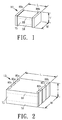
- the disclosed process for producing the chip-type SMD 10 of the present invention helps to improve accuracy of installation of a miniaturized SMD as compared to the prior art where a lead frame is used for packaging. More detailed speaking, the disclosed process is suitable for producing a miniaturized chip-type SMD 10, and more preferable for producing such a chip-type SMD 10 as shown in FIG. 1 that has a length (L) of 0.4-2.0mm, a width (W) of 0.2-1.3mm, and a thickness (T) of 0.2-0.8mm.
- the preferred specifications of the chip-type SMD 10 such made are listed in Table 1.
- Chip-Type SMD Number of outer electrodes Length (L) Width (W) Thickness (T) Model Number of Dies 01005 1-4 2 0.4 ⁇ 0.1mm 0.2 ⁇ 0.1mm Max 0.2mm 0201 1-4 2 0.6 ⁇ 0.1mm 0.3 ⁇ 0.1mm Max 0.3mm 0402 1-4 2 1.0 ⁇ 0.1mm 0.5 ⁇ 0.1mm Max 0.5mm 0603 1-4 2 1.6 ⁇ 0.1mm 0.8 ⁇ 0.1mm Max 0.7mm 0805 1-4 2 2.0 ⁇ 0.2mm 1.3 ⁇ 0.2mm Max 0.8mm
- the process for producing the chip-type SMD 10 mentioned above is also applicable to produce an array-type SMD 15 as shown in FIG. 2 of the present invention that has a length (L) of 1.0-2.4mm, a width (W) of 0.5-1.3mm, and a thickness (T) of 0.5-0.8mm.
- the preferred specifications of the array-type SMD 15 such made are listed in Table 2.
- the process for producing either the chip-type SMD 10 or the array-type SMD 15 of the present invention due to no use of lead-containing tin paste conforms to requirements for environmental protection.
- a chip-type SMD 10 is made from a single TVS diode D1.
- the SMD 10 such made has a single function of surge protection.
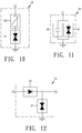
- a chip-type SMD 10 is made of two components including one TVS diode D1 of Example 1 and one PTC chip thermistor D2 that are connected in series.
- the SMD 10 such made has two functions by working as a temperature sensing switch and providing surge protection.
- a chip-type SMD 10 is made of two components including one TVS diode D1 of Example 1 and one capacitor chip D3 that are connected in parallel.
- the SMD 10 such made has two functions by providing surge protection and providing wave filtration.
- a chip-type SMD 10 is made of two components including one TVS diode D1 of Example 1 and one Schottky diode D4 that are connected in parallel.
- the SMD 10 such made has two functions by providing surge protection and providing backflow prevention.
- a chip-type SMD 10 is made of three components including one TVS diode D1 of Example 1, one PTC chip thermistor D2, and one fuse chip D5 that are connected in series.
- the SMD 10 such made has three functions by providing circuit cutout, working as temperature sensing switch, and providing surge protection.
- a chip-type SMD 10 is made of four components including one TVS diode D1 of Example 1 and one PTC chip thermistor D2 that are connected in series, as well as one capacitor chip D3 and one fuse chip D5 that are connected in series, wherein the two serial connections are further connected in parallel.
- the SMD 10 such made has four functions by working as a temperature sensing switch, providing surge protection, providing wave filtration, and providing circuit cutout.
- the SMD 10 is made of two dies of different functions that are connected either in parallel or in series.
- the SMDs such made each have two functions as listed in Table 3.
- Table 3 Example Die #1 Die #2 Package type Function 7
- the SMD 10 is made of three dies of different functions that are connected in parallel or in series.
- the SMD 10 such made each have three functions as listed in Table 4.
- Table 4 Example Die #1 Die #2 Die #3 Package type Function 15 TVS diode Resistor chip TVS diode Three dies Low-, high- and band-pass wave filtration Serial and parallel package 16 TVS diode Inductor chip TVS diode Three dies Low-, high- and band-pass wave filtration Serial and parallel package
Landscapes
- Engineering & Computer Science (AREA)
- Power Engineering (AREA)
- Microelectronics & Electronic Packaging (AREA)
- Manufacturing & Machinery (AREA)
- Lead Frames For Integrated Circuits (AREA)
- Physics & Mathematics (AREA)
- Electromagnetism (AREA)
- Thermistors And Varistors (AREA)
- Combinations Of Printed Boards (AREA)
- Casings For Electric Apparatus (AREA)
Applications Claiming Priority (1)
| Application Number | Priority Date | Filing Date | Title |
|---|---|---|---|
| TW104105626A TWI651830B (zh) | 2015-02-17 | 2015-02-17 | 多功能小型化表面黏著型電子元件及其製法 |
Publications (2)
| Publication Number | Publication Date |
|---|---|
| EP3059761A2 true EP3059761A2 (de) | 2016-08-24 |
| EP3059761A3 EP3059761A3 (de) | 2016-11-02 |
Family
ID=55405139
Family Applications (1)
| Application Number | Title | Priority Date | Filing Date |
|---|---|---|---|
| EP16155607.1A Withdrawn EP3059761A3 (de) | 2015-02-17 | 2016-02-12 | Oberflächenmontierbares bauelement mit einem oder mehreren chips zwischen zwei leiterplatten und verfahren zur herstellung davon |
Country Status (5)
| Country | Link |
|---|---|
| US (1) | US9443825B2 (de) |
| EP (1) | EP3059761A3 (de) |
| JP (1) | JP2016152416A (de) |
| KR (1) | KR101770729B1 (de) |
| TW (1) | TWI651830B (de) |
Cited By (1)
| Publication number | Priority date | Publication date | Assignee | Title |
|---|---|---|---|---|
| CN108683168A (zh) * | 2018-05-11 | 2018-10-19 | 杭州易龙防雷科技有限公司 | 一种具有阻燃功能的智能电涌保护器 |
Families Citing this family (22)
| Publication number | Priority date | Publication date | Assignee | Title |
|---|---|---|---|---|
| US9893058B2 (en) | 2015-09-17 | 2018-02-13 | Semiconductor Components Industries, Llc | Method of manufacturing a semiconductor device having reduced on-state resistance and structure |
| US11211359B2 (en) * | 2015-09-17 | 2021-12-28 | Semiconductor Components Industries, Llc | Semiconductor device and method of forming modular 3D semiconductor package with horizontal and vertical oriented substrates |
| US11373990B2 (en) * | 2016-02-29 | 2022-06-28 | Semtech Corporation | Semiconductor device and method of stacking semiconductor die for system-level ESD protection |
| CN108231699B (zh) * | 2016-12-09 | 2019-12-24 | 林慧敏 | 具有多个晶粒结构的覆晶封装二极管元件 |
| CN106783782A (zh) * | 2017-01-11 | 2017-05-31 | 广东百圳君耀电子有限公司 | 多引脚贴片元件及其制作方法 |
| KR20180094345A (ko) * | 2017-02-15 | 2018-08-23 | 주식회사 모다이노칩 | 칩 패키지 |
| TWI656612B (zh) * | 2017-03-16 | 2019-04-11 | Inpaq Technology Co., Ltd. | 半導體封裝件 |
| JP6773218B2 (ja) * | 2017-04-25 | 2020-10-21 | 株式会社村田製作所 | 電子部品 |
| KR102059442B1 (ko) * | 2017-08-22 | 2019-12-27 | 삼성전기주식회사 | 복합 전자부품, 그 실장 기판 |
| CN107565508B (zh) * | 2017-10-25 | 2019-09-27 | 四川中光防雷科技股份有限公司 | 具有失效分断功能的tvs防护器件 |
| CN108878270A (zh) * | 2017-11-09 | 2018-11-23 | 上海长园维安微电子有限公司 | 一种高功率密度tvs器件及其制造方法 |
| CN108231909A (zh) * | 2017-12-22 | 2018-06-29 | 中国振华集团永光电子有限公司(国营第八七三厂) | 一种高可靠超小型玻璃钝化复合二极管及其制备方法和应用 |
| TWI716680B (zh) * | 2018-04-16 | 2021-01-21 | 吳文湖 | 多段式雙串聯多晶組結構二極體元件 |
| KR102704159B1 (ko) * | 2018-09-07 | 2024-09-06 | 주식회사 아모텍 | 노이즈 제거용 복합소자 |
| DE102019108988B3 (de) | 2019-04-05 | 2020-08-13 | Infineon Technologies Ag | Leistungshalbleitermodul und verfahren zur herstellung desselben |
| TWI719517B (zh) * | 2019-06-27 | 2021-02-21 | 立昌先進科技股份有限公司 | 一種貼片式單顆小尺寸及陣列型之晶片半導體元件之封裝方法 |
| CN110379800A (zh) * | 2019-07-31 | 2019-10-25 | 中国振华集团永光电子有限公司(国营第八七三厂) | 一种陶瓷贴片封装双向低结电容tvs二极管 |
| CN110444537A (zh) * | 2019-08-29 | 2019-11-12 | 中国振华集团永光电子有限公司(国营第八七三厂) | 一种陶瓷贴片封装双向低结电容tvs二极管的设计方法 |
| KR102747646B1 (ko) | 2019-12-19 | 2024-12-27 | 삼성전자주식회사 | 반도체 패키지 및 그 제조방법 |
| KR102854678B1 (ko) | 2020-06-15 | 2025-09-04 | 삼성디스플레이 주식회사 | 시스템 인 패키지 및 이를 포함하는 전자 모듈 |
| US11335479B1 (en) * | 2021-01-06 | 2022-05-17 | Fuzetec Technology Co., Ltd. | Composite circuit protection device |
| CN113451233B (zh) * | 2021-05-14 | 2022-10-28 | 上海维攀微电子有限公司 | 一种tvs二极管封装结构 |
Family Cites Families (35)
| Publication number | Priority date | Publication date | Assignee | Title |
|---|---|---|---|---|
| JPS5013492Y1 (de) * | 1970-03-31 | 1975-04-24 | ||
| JP3048087B2 (ja) * | 1992-07-01 | 2000-06-05 | ローム株式会社 | 複合電子部品 |
| JPH08250645A (ja) * | 1995-03-08 | 1996-09-27 | Rohm Co Ltd | 半導体装置と増幅回路 |
| JPH08250648A (ja) * | 1995-03-08 | 1996-09-27 | Rohm Co Ltd | 半導体装置およびそれを用いた論理回路 |
| CN1155996C (zh) * | 1995-05-12 | 2004-06-30 | 皇家菲利浦电子有限公司 | 制造适于表面贴装的半导体器件的方法 |
| JP3447025B2 (ja) * | 1995-07-31 | 2003-09-16 | 日本インター株式会社 | 表面実装型電子部品及びその製造方法 |
| JP3698489B2 (ja) * | 1996-07-04 | 2005-09-21 | 株式会社ルネサステクノロジ | 電子部品 |
| JPH1079461A (ja) * | 1996-09-05 | 1998-03-24 | Hitachi Ltd | 半導体集積回路装置およびその製造方法 |
| JP3604108B2 (ja) * | 1997-02-17 | 2004-12-22 | 株式会社シチズン電子 | チップ型光半導体の製造方法 |
| US5994167A (en) * | 1997-05-21 | 1999-11-30 | Zowie Technology Corporation | Method of making a fiberglass reinforced resin plate |
| US6059173A (en) * | 1998-03-05 | 2000-05-09 | International Business Machines Corporation | Micro grid array solder interconnection structure for second level packaging joining a module and printed circuit board |
| US6236302B1 (en) * | 1998-03-05 | 2001-05-22 | Bourns, Inc. | Multilayer conductive polymer device and method of manufacturing same |
| JP4187278B2 (ja) * | 1998-07-08 | 2008-11-26 | 大日本印刷株式会社 | 非接触icカードおよびその製造方法 |
| KR100461718B1 (ko) * | 2002-03-18 | 2004-12-14 | 삼성전기주식회사 | 칩 패키지 및 그 제조방법 |
| JP2004165314A (ja) * | 2002-11-12 | 2004-06-10 | Toshiba Corp | 半導体装置およびその製造方法 |
| JP4082265B2 (ja) * | 2003-04-08 | 2008-04-30 | 松下電器産業株式会社 | 半導体装置の製造方法 |
| JP3759131B2 (ja) * | 2003-07-31 | 2006-03-22 | Necエレクトロニクス株式会社 | リードレスパッケージ型半導体装置とその製造方法 |
| JP2005260196A (ja) * | 2004-02-13 | 2005-09-22 | Origin Electric Co Ltd | 半導体装置の製造方法及び表面実装型半導体装置 |
| JP2005243685A (ja) * | 2004-02-24 | 2005-09-08 | Renesas Technology Corp | 半導体装置 |
| WO2006043388A1 (ja) * | 2004-10-21 | 2006-04-27 | Matsushita Electric Industrial Co., Ltd. | 半導体内蔵モジュール及びその製造方法 |
| KR20060103864A (ko) * | 2005-03-28 | 2006-10-04 | 타이코 일렉트로닉스 코포레이션 | Pptc 층들 사이에 능동 소자를 갖는 표면 장착식 다층전기 회로 보호 장치 |
| JP4614278B2 (ja) * | 2005-05-25 | 2011-01-19 | アルプス電気株式会社 | 電子回路ユニット、及びその製造方法 |
| JP5454834B2 (ja) * | 2007-08-30 | 2014-03-26 | 日立化成株式会社 | 粗化処理装置 |
| EP2453476A1 (de) * | 2010-11-12 | 2012-05-16 | Nxp B.V. | Verfahren zur Verkapselung eines Halbleiterbauelements und Halbleiterbauelementverkapselung |
| JP2012151406A (ja) * | 2011-01-21 | 2012-08-09 | Yazaki Corp | 半導体装置及びその製造方法 |
| US8363382B2 (en) * | 2011-02-10 | 2013-01-29 | Sfi Electronics Technology Inc. | Structure of multilayer ceramic device |
| WO2013005474A1 (ja) * | 2011-07-04 | 2013-01-10 | 本田技研工業株式会社 | 半導体装置 |
| DE102012202281A1 (de) * | 2012-02-15 | 2013-08-22 | Infineon Technologies Ag | Halbleiteranordnung für Druckkontaktierung |
| CN104603932A (zh) * | 2012-12-21 | 2015-05-06 | 松下知识产权经营株式会社 | 电子部件封装件及其制造方法 |
| EP2804209A1 (de) * | 2013-05-17 | 2014-11-19 | ABB Technology AG | Geformtes Elektronikmodul |
| KR102161173B1 (ko) * | 2013-08-29 | 2020-09-29 | 삼성전자주식회사 | 패키지 온 패키지 장치 및 이의 제조 방법 |
| TWI559576B (zh) * | 2013-11-05 | 2016-11-21 | 立昌先進科技股份有限公司 | A chip type diode package element and its manufacturing method |
| US9287240B2 (en) * | 2013-12-13 | 2016-03-15 | Micron Technology, Inc. | Stacked semiconductor die assemblies with thermal spacers and associated systems and methods |
| TWI501363B (zh) * | 2014-01-10 | 2015-09-21 | 立昌先進科技股份有限公司 | 一種小型化表面黏著型二極體封裝元件及其製法 |
| CN104637914B (zh) * | 2015-02-28 | 2018-02-13 | 立昌先进科技股份有限公司 | 多功能表面黏着型电子组件及其制法 |
-
2015
- 2015-02-17 TW TW104105626A patent/TWI651830B/zh active
-
2016
- 2016-02-04 KR KR1020160014264A patent/KR101770729B1/ko active Active
- 2016-02-08 JP JP2016021801A patent/JP2016152416A/ja active Pending
- 2016-02-09 US US15/018,896 patent/US9443825B2/en active Active
- 2016-02-12 EP EP16155607.1A patent/EP3059761A3/de not_active Withdrawn
Non-Patent Citations (1)
| Title |
|---|
| None |
Cited By (2)
| Publication number | Priority date | Publication date | Assignee | Title |
|---|---|---|---|---|
| CN108683168A (zh) * | 2018-05-11 | 2018-10-19 | 杭州易龙防雷科技有限公司 | 一种具有阻燃功能的智能电涌保护器 |
| CN108683168B (zh) * | 2018-05-11 | 2019-05-10 | 杭州易龙防雷科技有限公司 | 一种具有阻燃功能的智能电涌保护器 |
Also Published As
| Publication number | Publication date |
|---|---|
| JP2016152416A (ja) | 2016-08-22 |
| KR101770729B1 (ko) | 2017-09-05 |
| TW201631736A (zh) | 2016-09-01 |
| US20160240510A1 (en) | 2016-08-18 |
| KR20160101665A (ko) | 2016-08-25 |
| US9443825B2 (en) | 2016-09-13 |
| EP3059761A3 (de) | 2016-11-02 |
| TWI651830B (zh) | 2019-02-21 |
Similar Documents
| Publication | Publication Date | Title |
|---|---|---|
| US9443825B2 (en) | Multi-function miniaturized surface-mount device and process for producing the same | |
| KR101650896B1 (ko) | 소형화된 smd 다이오드 패키지 및 이를 생산하기 위한 공정 | |
| JP3689696B2 (ja) | チップパッケージの製造方法 | |
| CN101996766B (zh) | 电子部件及其制造方法 | |
| US20080239621A1 (en) | Clip-on leadframe | |
| JP5672678B2 (ja) | 電子部品及びその製造方法 | |
| KR19990029533A (ko) | 다중 소자 캐패시터 | |
| US8355240B2 (en) | Multilayer capacitor and method for adjusting equivalent series impedance of same | |
| US20080024998A1 (en) | Substrate structure integrated with passive components | |
| JP4233776B2 (ja) | 回路形成基板 | |
| CN104637914B (zh) | 多功能表面黏着型电子组件及其制法 | |
| US20080023821A1 (en) | Substrate structure integrated with passive components | |
| KR20150089213A (ko) | 칩 인덕터 | |
| TWI719517B (zh) | 一種貼片式單顆小尺寸及陣列型之晶片半導體元件之封裝方法 | |
| JPH05283283A (ja) | チップ型cr複合素子及びその製造方法 | |
| JP7252702B2 (ja) | 複合電子部品、複合電子部品包装体、及び回路基板 | |
| US10211157B2 (en) | Electronic component | |
| US7557425B2 (en) | Package cap with bypass capacitance | |
| JP2006019596A (ja) | 半導体装置およびその製造方法 | |
| JP2002299986A (ja) | 電子回路ユニット | |
| KR20140039653A (ko) | 와이어 본딩이 가능한 표면 실장 소자 및 반도체 패키지 | |
| JPH0613257A (ja) | チップ形コンデンサ | |
| Salisbury | Revolutionary approach in tantalum capacitor design which has made microminiature 0603 case size possible and improved electrical performance | |
| JP2005251956A (ja) | 半導体モジュール及びその製造方法 | |
| JPH07249540A (ja) | コンデンサアレー |
Legal Events
| Date | Code | Title | Description |
|---|---|---|---|
| PUAI | Public reference made under article 153(3) epc to a published international application that has entered the european phase |
Free format text: ORIGINAL CODE: 0009012 |
|
| AK | Designated contracting states |
Kind code of ref document: A2 Designated state(s): AL AT BE BG CH CY CZ DE DK EE ES FI FR GB GR HR HU IE IS IT LI LT LU LV MC MK MT NL NO PL PT RO RS SE SI SK SM TR |
|
| AX | Request for extension of the european patent |
Extension state: BA ME |
|
| PUAL | Search report despatched |
Free format text: ORIGINAL CODE: 0009013 |
|
| AK | Designated contracting states |
Kind code of ref document: A3 Designated state(s): AL AT BE BG CH CY CZ DE DK EE ES FI FR GB GR HR HU IE IS IT LI LT LU LV MC MK MT NL NO PL PT RO RS SE SI SK SM TR |
|
| AX | Request for extension of the european patent |
Extension state: BA ME |
|
| RIC1 | Information provided on ipc code assigned before grant |
Ipc: H05K 1/14 20060101ALI20160929BHEP Ipc: H05K 1/11 20060101ALI20160929BHEP Ipc: H05K 3/40 20060101ALI20160929BHEP Ipc: H01L 21/98 20060101ALI20160929BHEP Ipc: H01L 23/538 20060101ALI20160929BHEP Ipc: H01L 21/56 20060101ALI20160929BHEP Ipc: H01L 23/498 20060101AFI20160929BHEP Ipc: H01L 23/31 20060101ALI20160929BHEP Ipc: H01L 25/065 20060101ALI20160929BHEP |
|
| STAA | Information on the status of an ep patent application or granted ep patent |
Free format text: STATUS: THE APPLICATION HAS BEEN PUBLISHED |
|
| STAA | Information on the status of an ep patent application or granted ep patent |
Free format text: STATUS: THE APPLICATION IS DEEMED TO BE WITHDRAWN |
|
| 18D | Application deemed to be withdrawn |
Effective date: 20170503 |