EP3067723A1 - Methode de réglage d'un ou de plusieurs résonateurs - Google Patents
Methode de réglage d'un ou de plusieurs résonateurs Download PDFInfo
- Publication number
- EP3067723A1 EP3067723A1 EP15290070.0A EP15290070A EP3067723A1 EP 3067723 A1 EP3067723 A1 EP 3067723A1 EP 15290070 A EP15290070 A EP 15290070A EP 3067723 A1 EP3067723 A1 EP 3067723A1
- Authority
- EP
- European Patent Office
- Prior art keywords
- resonator
- wavelength
- photonic
- light
- resonance
- Prior art date
- Legal status (The legal status is an assumption and is not a legal conclusion. Google has not performed a legal analysis and makes no representation as to the accuracy of the status listed.)
- Withdrawn
Links
- 238000000034 method Methods 0.000 title claims abstract description 105
- 230000003287 optical effect Effects 0.000 claims abstract description 57
- 238000005530 etching Methods 0.000 claims abstract description 43
- 239000012530 fluid Substances 0.000 claims abstract description 32
- 230000008569 process Effects 0.000 claims abstract description 27
- 150000002500 ions Chemical class 0.000 claims abstract description 20
- 230000003247 decreasing effect Effects 0.000 claims abstract description 4
- 239000000463 material Substances 0.000 claims description 19
- 239000000758 substrate Substances 0.000 claims description 16
- 239000004065 semiconductor Substances 0.000 claims description 13
- 229910001218 Gallium arsenide Inorganic materials 0.000 claims description 11
- 238000010168 coupling process Methods 0.000 claims description 10
- 230000008878 coupling Effects 0.000 claims description 8
- 238000005859 coupling reaction Methods 0.000 claims description 8
- 239000007788 liquid Substances 0.000 claims description 8
- 230000005540 biological transmission Effects 0.000 claims description 5
- 239000004038 photonic crystal Substances 0.000 claims description 5
- 229910052710 silicon Inorganic materials 0.000 claims description 5
- 239000010703 silicon Substances 0.000 claims description 5
- 238000010408 sweeping Methods 0.000 claims description 5
- 230000007423 decrease Effects 0.000 claims description 4
- 239000003989 dielectric material Substances 0.000 claims description 3
- 238000002347 injection Methods 0.000 claims description 3
- 239000007924 injection Substances 0.000 claims description 3
- 238000002329 infrared spectrum Methods 0.000 claims description 2
- 238000001429 visible spectrum Methods 0.000 claims description 2
- JBRZTFJDHDCESZ-UHFFFAOYSA-N AsGa Chemical compound [As]#[Ga] JBRZTFJDHDCESZ-UHFFFAOYSA-N 0.000 description 11
- 238000001228 spectrum Methods 0.000 description 7
- 238000004519 manufacturing process Methods 0.000 description 6
- 230000003595 spectral effect Effects 0.000 description 5
- IJGRMHOSHXDMSA-UHFFFAOYSA-N Atomic nitrogen Chemical compound N#N IJGRMHOSHXDMSA-UHFFFAOYSA-N 0.000 description 4
- XUIMIQQOPSSXEZ-UHFFFAOYSA-N Silicon Chemical compound [Si] XUIMIQQOPSSXEZ-UHFFFAOYSA-N 0.000 description 4
- 238000002474 experimental method Methods 0.000 description 4
- 238000003491 array Methods 0.000 description 3
- 230000007246 mechanism Effects 0.000 description 3
- 238000010521 absorption reaction Methods 0.000 description 2
- 230000008901 benefit Effects 0.000 description 2
- 238000011161 development Methods 0.000 description 2
- 239000007789 gas Substances 0.000 description 2
- 229910052757 nitrogen Inorganic materials 0.000 description 2
- 238000011160 research Methods 0.000 description 2
- 239000002356 single layer Substances 0.000 description 2
- 230000001960 triggered effect Effects 0.000 description 2
- XLYOFNOQVPJJNP-UHFFFAOYSA-N water Substances O XLYOFNOQVPJJNP-UHFFFAOYSA-N 0.000 description 2
- 229910000980 Aluminium gallium arsenide Inorganic materials 0.000 description 1
- 229940095054 ammoniac Drugs 0.000 description 1
- 230000003321 amplification Effects 0.000 description 1
- 230000015572 biosynthetic process Effects 0.000 description 1
- 238000007664 blowing Methods 0.000 description 1
- 239000000969 carrier Substances 0.000 description 1
- 230000015556 catabolic process Effects 0.000 description 1
- 238000003486 chemical etching Methods 0.000 description 1
- 238000006243 chemical reaction Methods 0.000 description 1
- 239000011248 coating agent Substances 0.000 description 1
- 238000000576 coating method Methods 0.000 description 1
- 238000006731 degradation reaction Methods 0.000 description 1
- 230000000593 degrading effect Effects 0.000 description 1
- 239000008367 deionised water Substances 0.000 description 1
- 229910021641 deionized water Inorganic materials 0.000 description 1
- 230000001934 delay Effects 0.000 description 1
- 238000004090 dissolution Methods 0.000 description 1
- 230000005684 electric field Effects 0.000 description 1
- 230000005520 electrodynamics Effects 0.000 description 1
- 238000005516 engineering process Methods 0.000 description 1
- 230000002708 enhancing effect Effects 0.000 description 1
- 230000005284 excitation Effects 0.000 description 1
- 239000000835 fiber Substances 0.000 description 1
- 238000009434 installation Methods 0.000 description 1
- 239000012212 insulator Substances 0.000 description 1
- 230000003993 interaction Effects 0.000 description 1
- 150000008040 ionic compounds Chemical class 0.000 description 1
- 230000031700 light absorption Effects 0.000 description 1
- 238000012544 monitoring process Methods 0.000 description 1
- NJPPVKZQTLUDBO-UHFFFAOYSA-N novaluron Chemical compound C1=C(Cl)C(OC(F)(F)C(OC(F)(F)F)F)=CC=C1NC(=O)NC(=O)C1=C(F)C=CC=C1F NJPPVKZQTLUDBO-UHFFFAOYSA-N 0.000 description 1
- 238000003199 nucleic acid amplification method Methods 0.000 description 1
- 239000013307 optical fiber Substances 0.000 description 1
- 238000000206 photolithography Methods 0.000 description 1
- 238000001020 plasma etching Methods 0.000 description 1
- 229920000642 polymer Polymers 0.000 description 1
- 230000007425 progressive decline Effects 0.000 description 1
- 238000012827 research and development Methods 0.000 description 1
- 230000002441 reversible effect Effects 0.000 description 1
- 238000004088 simulation Methods 0.000 description 1
- 241000894007 species Species 0.000 description 1
- 238000004611 spectroscopical analysis Methods 0.000 description 1
- 239000010409 thin film Substances 0.000 description 1
- 230000007704 transition Effects 0.000 description 1
- 238000000411 transmission spectrum Methods 0.000 description 1
Images


Classifications
-
- G—PHYSICS
- G02—OPTICS
- G02B—OPTICAL ELEMENTS, SYSTEMS OR APPARATUS
- G02B27/00—Optical systems or apparatus not provided for by any of the groups G02B1/00 - G02B26/00, G02B30/00
- G02B27/0012—Optical design, e.g. procedures, algorithms, optimisation routines
-
- G—PHYSICS
- G02—OPTICS
- G02B—OPTICAL ELEMENTS, SYSTEMS OR APPARATUS
- G02B5/00—Optical elements other than lenses
- G02B5/18—Diffraction gratings
- G02B5/1847—Manufacturing methods
- G02B5/1857—Manufacturing methods using exposure or etching means, e.g. holography, photolithography, exposure to electron or ion beams
-
- G—PHYSICS
- G02—OPTICS
- G02B—OPTICAL ELEMENTS, SYSTEMS OR APPARATUS
- G02B6/00—Light guides; Structural details of arrangements comprising light guides and other optical elements, e.g. couplings
- G02B6/10—Light guides; Structural details of arrangements comprising light guides and other optical elements, e.g. couplings of the optical waveguide type
- G02B6/12—Light guides; Structural details of arrangements comprising light guides and other optical elements, e.g. couplings of the optical waveguide type of the integrated circuit kind
- G02B6/12007—Light guides; Structural details of arrangements comprising light guides and other optical elements, e.g. couplings of the optical waveguide type of the integrated circuit kind forming wavelength selective elements, e.g. multiplexer, demultiplexer
-
- G—PHYSICS
- G02—OPTICS
- G02B—OPTICAL ELEMENTS, SYSTEMS OR APPARATUS
- G02B6/00—Light guides; Structural details of arrangements comprising light guides and other optical elements, e.g. couplings
- G02B6/10—Light guides; Structural details of arrangements comprising light guides and other optical elements, e.g. couplings of the optical waveguide type
- G02B6/12—Light guides; Structural details of arrangements comprising light guides and other optical elements, e.g. couplings of the optical waveguide type of the integrated circuit kind
- G02B6/13—Integrated optical circuits characterised by the manufacturing method
- G02B6/136—Integrated optical circuits characterised by the manufacturing method by etching
-
- G—PHYSICS
- G02—OPTICS
- G02B—OPTICAL ELEMENTS, SYSTEMS OR APPARATUS
- G02B6/00—Light guides; Structural details of arrangements comprising light guides and other optical elements, e.g. couplings
- G02B6/24—Coupling light guides
- G02B6/26—Optical coupling means
- G02B6/28—Optical coupling means having data bus means, i.e. plural waveguides interconnected and providing an inherently bidirectional system by mixing and splitting signals
- G02B6/293—Optical coupling means having data bus means, i.e. plural waveguides interconnected and providing an inherently bidirectional system by mixing and splitting signals with wavelength selective means
- G02B6/29331—Optical coupling means having data bus means, i.e. plural waveguides interconnected and providing an inherently bidirectional system by mixing and splitting signals with wavelength selective means operating by evanescent wave coupling
- G02B6/29335—Evanescent coupling to a resonator cavity, i.e. between a waveguide mode and a resonant mode of the cavity
- G02B6/29338—Loop resonators
- G02B6/29341—Loop resonators operating in a whispering gallery mode evanescently coupled to a light guide, e.g. sphere or disk or cylinder
-
- G—PHYSICS
- G02—OPTICS
- G02B—OPTICAL ELEMENTS, SYSTEMS OR APPARATUS
- G02B1/00—Optical elements characterised by the material of which they are made; Optical coatings for optical elements
- G02B1/002—Optical elements characterised by the material of which they are made; Optical coatings for optical elements made of materials engineered to provide properties not available in nature, e.g. metamaterials
- G02B1/005—Optical elements characterised by the material of which they are made; Optical coatings for optical elements made of materials engineered to provide properties not available in nature, e.g. metamaterials made of photonic crystals or photonic band gap materials
-
- G—PHYSICS
- G02—OPTICS
- G02B—OPTICAL ELEMENTS, SYSTEMS OR APPARATUS
- G02B5/00—Optical elements other than lenses
- G02B5/20—Filters
- G02B5/28—Interference filters
-
- G—PHYSICS
- G02—OPTICS
- G02B—OPTICAL ELEMENTS, SYSTEMS OR APPARATUS
- G02B6/00—Light guides; Structural details of arrangements comprising light guides and other optical elements, e.g. couplings
- G02B6/24—Coupling light guides
- G02B6/26—Optical coupling means
- G02B6/28—Optical coupling means having data bus means, i.e. plural waveguides interconnected and providing an inherently bidirectional system by mixing and splitting signals
- G02B6/293—Optical coupling means having data bus means, i.e. plural waveguides interconnected and providing an inherently bidirectional system by mixing and splitting signals with wavelength selective means
- G02B6/29331—Optical coupling means having data bus means, i.e. plural waveguides interconnected and providing an inherently bidirectional system by mixing and splitting signals with wavelength selective means operating by evanescent wave coupling
- G02B6/29335—Evanescent coupling to a resonator cavity, i.e. between a waveguide mode and a resonant mode of the cavity
- G02B6/29338—Loop resonators
Definitions
- the invention relates to the field of micro- and nano-photonic resonators and in particular to the tuning of such resonators to a desired wavelength.
- Optical resonators which are part of a photonic device, generally consist in a cavity in which light can enter and resonate, hereby amplifying the signal.
- Micro- and nanoresonators are small devices, which are difficult to build with a high precision.
- Industrials have developed clean room fabrication techniques (such as photolithography and plasma etching) that typically result in a precision no better than a few nanometers. These reproducibility constraints due to the manufacturing-related imprecisions ultimately affect the ultimate resonance wavelength of the fabricated optical resonators. As a result, fabricating several high Q, wavelength-sized optical resonators sharing exactly the same resonance wavelength is not currently achievable, even through state-of-the art fabrication means.
- Those resonators have several applications, either in academic research or in industrial development for improved technology.
- Light-matter interaction (lasers, cavity electrodynamics, optomechanics, non-linear optics, ...) is a major topic of current research.
- Obtaining optical resonators with precise resonance frequencies, which can couple to given atomic transitions or molecular excitations is of interest.
- arrays of resonators and their collective behavior are also a subject of interest.
- Miniaturized optical resonators are currently the focus of important research and development, with applications in optical delays, optical routing with micro-nanoscale devices, photonic force and gas sensing, optical gyroscopes, Silicon On Insulator optical devices, semiconductor lasers, optical computers, optical metamaterials.
- Resonators can be also used as:
- the method of the invention may comprise the following features in combination or not.
- the photonic resonator has a bandgap wavelength set by its constitutive material and the wavelength of the injected light is above the resonator bandgap wavelength.
- the tuning procedure consists in lowering the resonance wavelength of the photonic resonator by consecutive sweeps, each sweep consisting in sweeping the light wavelength of the injected light between values which comprise the resonance wavelength of the photonic resonator.
- the step of injecting light is realized by far-field or near-field optical coupling technique, and where light is injected into one or several resonators.
- the step of injecting light is implemented by a waveguide which is on a substrate onto which the photonic resonator is positioned, the waveguide being in the vicinity of the photonic resonator in order to allow near-field optical coupling between the two, the light wavelength of the injected light being larger than a material bandgap wavelength.
- the light wavelength of the injected light is comprised amongst visible and infrared spectrum.
- the coupling between the photonic resonator and the waveguide is achieved by evanescent waves.
- the fluid is a liquid containing ions.
- the method presented here allows for three orders of magnitude higher precision, both in controlling the effective optical device size and in its spectral resonance, reaching picometer precision for these two aspects.
- the method is applicable to an industrial setting: it is permanent, scalable and fast, requires little equipment.
- the permanence of the tuning is a major advantage for an industrial application, and the method allows for a broad range of wavelength tuning, from picometers to hundreds of nanometers.
- the method does not require any additional component on the photonic device (polymer coating, electrical connects, thermal controls, as explained before), making it simple and non-degrading.
- the surrounding fluid can easily be removed after the tuning step without damaging the characteristics of the resonator.
- the method of the invention allows tuning several resonators, each one having a different resonance wavelength.
- this method comprises the following steps:
- This method is thus scalable to a large number of photonic devices and still requires a single tuning step and a short amount of time (order of the minute), therefore overwhelming the drawbacks of the prior art.
- the tuning step automatically etches the photonic devices of largest size, and then automatically etches all the cavities of identical size at identical speed, provides a fast tuning mechanism and does not require the one-by-one identification of the numerous resonators involved in a collective architecture.
- the invention concerns a photonic device comprising at least one micro and/or nanophotonic resonator (10) on the substrate (30), obtainable by a method according to the first aspect or the second aspect of the invention.
- the photonic device may be tuned with a physical precision of dimensions of the photonic resonator less than 10pm.
- the photonic device may be tuned at the same value with a physical precision of dimensions of the photonic resonators less than 10pm.
- the photonic device may comprise a waveguide which enables transmission of the light to each photonic resonator, by being on the substrate in the vicinity of the at least one resonator.
- Each photonic resonator is a disk, a photonic crystal resonator, a ring or racetrack resonator, a Bragg resonator, a distributed feedback grating resonator, a Fabry-Perot resonator or a plasmonic resonator.
- the photonic resonator, the substrate and the waveguide are made of GaAs, Silicon, and/or any other semi-conductor and dielectric material where photoelectrochemical etching operates.
- resonator it is meant any kind, or any shape, or any material that would enable a photonic resonance and the confinement of light in a given volume.
- the photonic device The photonic device
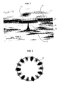
- the nano- or micro-photonic resonant cavities, or photonic resonators 10, hereby referred as the resonator 10, employed here for proof of principle experiments consist of disks 11 (see figure 1 ), made from a semi-conductor such as Gallium Arsenide (GaAs).
- GaAs Gallium Arsenide
- a disk is typically micrometer-sized in lateral dimensions and few hundreds of nanometers thick.
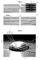
- the resonator 10 is coupled to an integrated optical waveguide 20, whose central region 21 is tapered in the vicinity of the resonator 10 to allow optical coupling. Typically, and not only in the disk case, said coupling is achieved by evanescent waves.
- the waveguide 20 enables transmission of the light from an external light source to the resonator 10. For instance, the distance between the waveguide 20 and the disk 11 is between 100 to 800 nm (hundred to eight hundred nanometers).
- An Aluminium Gallium Arsenide pedestal 12 isolates the disk 11 from a sample substrate 30 onto which the waveguide 20 is positioned.
- Resonators 10, waveguides 20 and the substrate 30 will be referred as the photonic device.
- the photonic resonator 10 has an energy bandgap set by its constitutive material.
- a bandgap wavelength lambda_B is associated to said bandgap set. Light whose energy is below the energy bandgap is generally not absorbed.
- the bandgap wavelength lambda_B is around 870 nm, and GaAs becomes transparent to wavelengths above that.
- the GaAs disk 11 supports high quality optical Whispering Gallery Modes (WGMs), which correspond to a type of wave that can travel around a concave surface (see figure 2 ). As shown in figure 3 , the resonance associated to WGMs appear as dips in an optical spectrum. Such disk resonator 10 typically presents an optical resonance doublet. For clarity reasons in the description, this doublet will sometimes be considered as a single resonance value ⁇ r.
- Q Quality factor
- ⁇ r is a resonance wavelength of the resonator and ⁇ is the mode resonance full width at half maximum (FWHM).
- FWHM full width at half maximum
- Wavelength ⁇ is variable and the laser source 40 delivers preferably monochromatic light.
- the optical spectroscopy of the resonator 10 and waveguide 20 is performed in the present case in the 1260-1350 nanometers wavelength range (infrared) using the laser source 40 which is in the present case a continuous wave external cavity diode laser.
- the beam of laser light is focused onto the coupling waveguide input facet 22 using a micro-lensed fiber 41.
- Output light at the waveguide output facet 23 is collected by a microscope objective 42 and sent on a photodetector 43 (see path on figure 4 ).
- the several dips appearing in the transmission spectrum correspond to the WGMs of the disk 11 of the resonator 10. Linewidths are about 20 to 50 pm.
- the optical quality factor Q is about 70 000 to 25000.
- On figure 5 is represented a plurality of resonators 10 and waveguides 20 on the sample substrate 30. There is only one resonator 10 per waveguide 20.
- On figure 6 is represented a collective architecture of resonators 10 and waveguides 20 on the sample substrate. As it can be observed, three resonators 10a, 10b, 10c are located in the tapered central region 21 of each waveguide 20, said three resonators 10 being thus optically fed by the same waveguide 20.
- each resonator 10 has its resonance wavelengths ⁇ r, which are to be tuned at a targeted resonance wavelength ⁇ t.
- Each resonance wavelength ⁇ r depends on the dimension of the resonator 10. In the present case, we remind that each resonator 10 has in fact two resonance wavelength ⁇ r corresponding to the doublet, but as the two values are bound, we can refer to a single one.
- the method for tuning resonator(s) relies upon photoelectrochemical (PEC) etching.
- PEC is a light activated chemical etching. To enable such an etching, the resonator 10 has to be immersed in a fluid 60 containing ions (see figure 6 ).
- the photonic device in particular the resonators 10a, 10b are immersed in the fluid 60 containing ions.
- a preliminary step E0 is thus to deposit a droplet of said fluid 60 onto the resonator 10, or more generally to immerse resonators in the said fluid.
- the resonators 10 are thus surrounded by said fluid 60.
- the method comprises a step of injecting light into the resonator 10 at the resonance, that is to say the wavelength ⁇ of the injected light is equal or sensibly equal to the resonator wavelength ⁇ r, such that the injected light ⁇ resonates within the resonator 10 and triggers a photoelectrochemical etching (PEC) process.
- PEC photoelectrochemical etching
- the resonance amplifies light intensity in the resonator 10 and in particular in the disk 11, hereby enhancing the etching process.
- the presence of surrounding fluid 60 containing ions enables such process.
- the disk is etched, its dimensions decrease, hereby lowering the resonance wavelength ⁇ r of the resonator 10.
- the etching process stops.
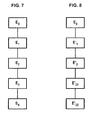
- the previous step is part of the following ones:
- the wavelength ⁇ of the injected light is above the resonator bandgap wavelength lambda_B. This means that the light energy is below the bandgap energy of the material.
- standard PEC etching technique consists in illuminating a semiconductor immersed in an electrically conductive liquid, such as the fluid 60 containing ions, with light whose energy is above the bandgap. This generates electrons and holes within the material and these photogenerated free carriers lead to the formation of ionic species at the surface of the semiconductor that are dissolved in the presence of ions provided by the fluid 60.
- an electrically conductive liquid such as the fluid 60 containing ions
- UV light that is to say light with a wavelength below 400nm
- UV light is often used because it is absorbed by the semi-conductor thanks to its energy above the energy bandgap of the resonator.
- visible light with energy above the bandgap can be used as well.
- light whose wavelength ⁇ is above the wavelength bandgap lambda B i.e. light whose energy is below the energy bandgap
- Infrared light is preferably used (light wavelength above 800 nanometers), but visible light (light wavelength between 400 and 800 nanometers) can be used as well, depending on the characteristics of the material of the resonator(s) to be etched and tuned.
- Semi-conductor resonator 10 in the present case GaAs disk 11, absorbs a residual fraction of the confined infrared light even at energy below the energy bandgap due to various mechanisms. Among those mechanisms are mid-gap levels present at the semi-conductor surface, as well as two-photon absorption at higher light intensity.
- the resonance increases the intensity of the injected light at the level of the resonator 10 and enables the etching process described above, even though the injected light wavelength ⁇ has its energy below the energy bandgap of the material. Indeed, the etching process is enabled thanks to the resonance of the resonator 10.
- a second aspect of the method is to tune several resonators 10a, 10b, 10c at a common targeted wavelength ⁇ t.
- the resonators 10a, 10b, 10c are typically coupled to a waveguide 20 (see figure 6 for instance)
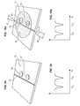
- Figures 9a to 11b show the principle of the method applied to a plurality of resonators.
- the photonic resonators 10a, 10b After micro-nanofabrication, the photonic resonators 10a, 10b have different size due to fabrication variability (see figure 9a ), and therefore express different resonance wavelength ⁇ ra and ⁇ rb (see figure 9b ), one being higher than the other one (for instance in this example resonator 10b is initially slightly larger than resonator 10a, hence ⁇ rb> ⁇ ra).
- This method is based on the first method previously described, that is to say a photoelectrical etching process triggered by optical resonance and a progressive decrease of the injected light wavelength ⁇ so as to shift the resonance wavelength ⁇ r to the targeted wavelength ⁇ t.
- the photonic device in particular the resonators 10a and 10b, are immersed in the fluid 60 containing ions (see figure 10a ).
- the same preliminary step E0 deposit a droplet of said fluid onto the resonator 10, or more generally immersing in the ionic fluid) is achieved.
- the next step consists in setting (E1') a light wavelength ⁇ of the injected light to a value larger than the resonance wavelengths ⁇ ra, ⁇ rb of the resonators 10.
- the laser source 40 is coupled to the waveguide 20.
- the light wavelength ⁇ is lowered (E2') so as to reach the first resonance wavelength ⁇ rb of the photonic resonator 10b.
- the etching process starts on this latter resonator. Due to the site-specific character of the method, the other resonator 10a, whose resonance wavelength ⁇ ra is lower, is not etched and remains intact.
- the injected light naturally enters first the resonance of resonator 10b and shifts its resonance wavelength ⁇ rb towards lower values (see arrow in figure 10b ).
- the next step consists in lowering (E31') the wavelength ⁇ of the injected light, so as to follow resonance wavelength ⁇ rb of the resonator 10b, which is decreasing because of the etching.
- the wavelength ⁇ is lowered until the resonance wavelength ⁇ rb of the resonator 10b reaches the resonance wavelength ⁇ ra of the other resonator 10a (see figures 11a , 11b ).
- both resonators 10a, 10b share a common resonance wavelength and the same dimensions, meaning that they are tuned.
- the process can be completed by lowering (E32') again the wavelength ⁇ of the injected light, which triggers the etching of both photonic resonators 10a, 10b at the same time and the same speed. It is therefore possible to reach the targeted resonance wavelength ⁇ t for both resonators 10a, 10b. Indeed, when the two resonances overlap, any further decrease of the injected light wavelength ⁇ simultaneously etches both resonators 10a, 10b and maintains them with exactly the same effective dimensions and optical resonance values.
- This method can be applied for tuning any number of resonators 10 coupled to a waveguide 20, as long as the value of the wavelength ⁇ of the injected light is above the highest resonance value ⁇ r of said resonators.
- the order in which the resonators 10 are positioned along the waveguide is not important, thanks to the wavelength selective nature of the tuning.
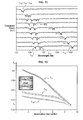
- Figures 12 shows the spectrum of resonance of resonators 10a, 10b, 10c being tuned.
- Each resonator 10 is associated to a resonant doublet.
- ⁇ ra, ⁇ rb, ⁇ rc for each resonator 10.
- Figure 13 shows the convergence of said resonant doublet wavelength towards a unique value, which is the targeted wavelength ⁇ t (again, the two close curves represent the resonant doublet).
- the first technique for tuning at a targeted wavelength ⁇ t with successive sweeps of laser ⁇ can be the following one:
- the second technique for tuning at a targeted wavelength ⁇ t can use a continuous shift of the laser source wavelength ⁇ .
- a laser source 40 must be chosen whose wavelength is continuously adjustable. The process consists in a unique and slow sweep.
- a control unit 50 can be connected to the laser source 40 so as to control the wavelength of the laser source 40 in order to precisely follow the resonance wavelength ⁇ r.
- the adjustment of the light wavelength typically consists in lowering the wavelength ⁇ , as long as the starting wavelength has been chosen above the highest resonance wavelength ⁇ r of the resonators 10.
- the fluid 60 is typically deposited as a microliter droplet of water on the sample substrate with a micro-pipette. This droplet covers several adjacent resonator and waveguides (see figure 6 , 10a ). Besides, such a fluid 60 leaves the overall optical transmission through waveguides unaltered in average power.
- the fluid 60 can be, as non-limitative example, a liquid containing a few ions, such as deionized water or ammoniac, or a gas containing ions, such as steam.
- the fluid 60 In order to be efficient, the fluid 60 must have a non-zero conductivity, that is to say an ability to conduct an electric current. As explained below, the value of said conductivity is not of a major importance.
- the fluid 60 can be easily removed after the tuning procedure by blowing air or nitrogen, without any damage to the photonic device.
- the resonant PEC tuning of optical resonators is not restricted to GaAs resonators shown above as example. Indeed the PEC process operates on all semiconductor materials in the standard configuration of light wavelength ⁇ below the material bandgap wavelength lambda B. Hence the technique presented here of PEC-assisted optical tuning applies to optical resonators fabricated out of any semiconductor material, with the specificity of now having the laser light wavelength ⁇ larger than the bandgap wavelength lambda B.
- the technique extends as well to dielectric optical resonators, even if PEC processes are less trivial to use in such materials, because of constraints due to the high bandgap energy of these materials.
- the technique also operates on different geometries of optical resonators, and not only on disk resonators sustaining WGMs like discussed above.
- optical resonators Of technological relevance are photonic crystal micro and nano-resonators, race-track and ring optical resonators, plasmonic resonators, Fabry-Perot resonators, Bragg mirror resonators and distributed feedback grating resonators. Any micro or nano-optical resonator providing optical resonance, with the associated light confinement and amplification, is suited for the technique.
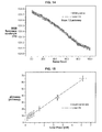
- the injected light has been injected discontinuously, by sweeping the laser source 40 several times back and forth across one optical resonance of the resonator 10. This way, at each sweep, a small and reproducible amount of energy was injected inside the resonator 10 (nano Joule range).
- the WGM resonance wavelength ⁇ r has been represented as a function of the sweep count.
- the power of the laser source 40 was low, at 0,2 mW at the display of the laser source controller. It has been estimated that a rate of 7 pm per round-trip sweep, i.e. 3.5 pm per single sweep has been achieved. This corresponds to the removal of the order of 10 -2 monolayer of material per sweep (for instance, one monolayer of GaAs is approximatively 300 pm).
- the error bar represents the 20 pm relative wavelength accuracy of the employed laser source 40 over repeated wavelength sweeps.
- the wavelength shift per sweep has been represented as a function of the laser power.
- a linear dependence can be observed; therefore the etching speed can be precisely controlled by controlling the power of the laser source 40. Several orders of magnitude in the etching speed are possible.
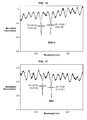
- the quality factors of the doublet of resonator 10 before the tuning are around 42 000 / 42 000 ( ⁇ r ⁇ 1334 nm and ⁇ ⁇ 32 pm for both dips of the doublet) and the quality factors afterwards are around 53 000 / 70 000 ( ⁇ r ⁇ 1330 nm and ⁇ ⁇ 25 pm and 19 pm for the dips of the doublet).
- the method does not damage the properties of the resonators 10, and would even improve their optical quality factor Q.
- the resonators are permanently tuned, even when the tuning laser is switched off and the fluid removed.
- the photonic devices, especially the resonators 10 are thus permanently tuned with a physical precision on the dimensions which is less than 10 pm, more precisely less than 4 pm. This means that, for each resonator, an absolute precision at less than 10pm can be reached. For several resonators, a relative precision of few tens of pm is demonstrated and less than 10 pm can be reached.
- the methods provide a high spatial selectivity: the resonator 10 is selectively etched while its nearby environment, such as the waveguide 20, the substrate 30, or other resonator of different resonance wavelength remain intact.
- a high quality factor resonator 10 can be tuned to resonance with a high precision.
- several resonators of high quality factor Q can be tuned to resonance as well. Thanks to the scalability of the method, hundreds of resonators can be rapidly tuned using a single sweep of laser wavelength ⁇ . Indeed, as described above, there is no need to identify and to act individually on each resonator; instead, the method automatically brings optical resonances at a common targeted wavelength ⁇ t, with a precision less that 10pm.
- the resonators 10 that can be tuned with those methods, one can cite photonic crystal resonators, Bragg resonators or plasmonic resonators.
- the resonator 10, the waveguide 20 and the substrate 30 can be also made of Silicon, or any other semi-conductor or dielectric material with a bandgap where photoelectrochemical (PEC) etching operates.
- PEC photoelectrochemical
Landscapes
- Physics & Mathematics (AREA)
- General Physics & Mathematics (AREA)
- Optics & Photonics (AREA)
- Engineering & Computer Science (AREA)
- Microelectronics & Electronic Packaging (AREA)
- Manufacturing & Machinery (AREA)
- Optical Integrated Circuits (AREA)
Priority Applications (7)
| Application Number | Priority Date | Filing Date | Title |
|---|---|---|---|
| EP15290070.0A EP3067723A1 (fr) | 2015-03-13 | 2015-03-13 | Methode de réglage d'un ou de plusieurs résonateurs |
| JP2017566198A JP6816037B2 (ja) | 2015-03-13 | 2016-03-04 | 一または複数の共振器をチューニングする方法 |
| PCT/EP2016/054704 WO2016146409A1 (fr) | 2015-03-13 | 2016-03-04 | Procédé permettant de syntoniser un ou plusieurs résonateurs |
| EP16708992.9A EP3268783B1 (fr) | 2015-03-13 | 2016-03-04 | Methode de réglage d'un ou de plusieurs résonateurs |
| KR1020177029335A KR20180019065A (ko) | 2015-03-13 | 2016-03-04 | 하나 이상의 공진기(들)를 동조하는 방법 |
| US15/557,950 US9995929B2 (en) | 2015-03-13 | 2016-03-04 | Method for tuning one or more resonator(s) |
| CN201680015616.3A CN107430244B (zh) | 2015-03-13 | 2016-03-04 | 使用一个或多个谐振器的方法 |
Applications Claiming Priority (1)
| Application Number | Priority Date | Filing Date | Title |
|---|---|---|---|
| EP15290070.0A EP3067723A1 (fr) | 2015-03-13 | 2015-03-13 | Methode de réglage d'un ou de plusieurs résonateurs |
Publications (1)
| Publication Number | Publication Date |
|---|---|
| EP3067723A1 true EP3067723A1 (fr) | 2016-09-14 |
Family
ID=53491460
Family Applications (2)
| Application Number | Title | Priority Date | Filing Date |
|---|---|---|---|
| EP15290070.0A Withdrawn EP3067723A1 (fr) | 2015-03-13 | 2015-03-13 | Methode de réglage d'un ou de plusieurs résonateurs |
| EP16708992.9A Active EP3268783B1 (fr) | 2015-03-13 | 2016-03-04 | Methode de réglage d'un ou de plusieurs résonateurs |
Family Applications After (1)
| Application Number | Title | Priority Date | Filing Date |
|---|---|---|---|
| EP16708992.9A Active EP3268783B1 (fr) | 2015-03-13 | 2016-03-04 | Methode de réglage d'un ou de plusieurs résonateurs |
Country Status (6)
| Country | Link |
|---|---|
| US (1) | US9995929B2 (fr) |
| EP (2) | EP3067723A1 (fr) |
| JP (1) | JP6816037B2 (fr) |
| KR (1) | KR20180019065A (fr) |
| CN (1) | CN107430244B (fr) |
| WO (1) | WO2016146409A1 (fr) |
Cited By (1)
| Publication number | Priority date | Publication date | Assignee | Title |
|---|---|---|---|---|
| EP3575784A1 (fr) * | 2018-05-28 | 2019-12-04 | Consejo Superior de Investigaciones Cientificas (CSIC) | Procédé et système d'analyse d'analytes par transduction de résonance mécanique |
Families Citing this family (4)
| Publication number | Priority date | Publication date | Assignee | Title |
|---|---|---|---|---|
| KR102697425B1 (ko) * | 2017-02-02 | 2024-08-21 | 삼성전자주식회사 | 분광기 및 그 분광기가 적용된 성분 측정 장치 |
| CN109343174B (zh) * | 2018-10-24 | 2020-07-10 | 中南民族大学 | 一种多通道多模式复用波导交叉及其制备方法 |
| EP3650833A1 (fr) * | 2018-11-09 | 2020-05-13 | Technische Universität München | Résonateur optique multicolore pour procédés d'imagerie |
| CN110212078B (zh) * | 2019-06-14 | 2020-10-27 | 厦门大学 | 一种电注入微盘谐振腔发光器件及其制备方法 |
Citations (3)
| Publication number | Priority date | Publication date | Assignee | Title |
|---|---|---|---|---|
| WO2002025338A2 (fr) * | 2000-09-22 | 2002-03-28 | Massachusetts Institute Of Technology | Procedes de modification de la resonance de micro-resonateurs a guide d'onde |
| EP1585087A1 (fr) | 2004-03-30 | 2005-10-12 | Canon Kabushiki Kaisha | Dispositif d 'affichage, dispositif d'observation d'image et dispositif de projection l'utilisant |
| US20140321502A1 (en) | 2013-06-11 | 2014-10-30 | National Institute Of Standards And Technology | Optical temperature sensor and use of same |
Family Cites Families (11)
| Publication number | Priority date | Publication date | Assignee | Title |
|---|---|---|---|---|
| FR2527865A1 (fr) * | 1982-06-01 | 1983-12-02 | Cepe | Resonateur piezo-electrique a haute frequence et son procede de fabrication |
| JPH07118624B2 (ja) * | 1990-11-28 | 1995-12-18 | キンセキ株式会社 | 圧電素子の周波数調整装置および周波数調整方法 |
| JPH10126186A (ja) * | 1996-10-16 | 1998-05-15 | Matsushita Electric Ind Co Ltd | 水晶振動子の周波数調整装置 |
| US6884740B2 (en) * | 2001-09-04 | 2005-04-26 | The Regents Of The University Of California | Photoelectrochemical undercut etching of semiconductor material |
| US20050148065A1 (en) * | 2003-12-30 | 2005-07-07 | Intel Corporation | Biosensor utilizing a resonator having a functionalized surface |
| US7396431B2 (en) * | 2004-09-30 | 2008-07-08 | Tokyo Electron Limited | Plasma processing system for treating a substrate |
| KR20100127376A (ko) * | 2009-05-26 | 2010-12-06 | 한국전자통신연구원 | 광 소자 및 그 형성방법 |
| EP2625556A2 (fr) * | 2010-10-08 | 2013-08-14 | Cornell University | Appareils, procédés et applications de piégeage optique utilisant des résonateurs à cristaux photoniques |
| US9690029B2 (en) | 2013-01-30 | 2017-06-27 | Cree, Inc. | Optical waveguides and luminaires incorporating same |
| CN103472129B (zh) * | 2013-09-17 | 2017-01-11 | 天津大学 | 用于流体环境检测的谐振传感器 |
| US9627199B2 (en) * | 2013-12-13 | 2017-04-18 | University Of Maryland, College Park | Methods of fabricating micro- and nanostructure arrays and structures formed therefrom |
-
2015
- 2015-03-13 EP EP15290070.0A patent/EP3067723A1/fr not_active Withdrawn
-
2016
- 2016-03-04 JP JP2017566198A patent/JP6816037B2/ja active Active
- 2016-03-04 EP EP16708992.9A patent/EP3268783B1/fr active Active
- 2016-03-04 US US15/557,950 patent/US9995929B2/en active Active
- 2016-03-04 KR KR1020177029335A patent/KR20180019065A/ko not_active Ceased
- 2016-03-04 CN CN201680015616.3A patent/CN107430244B/zh active Active
- 2016-03-04 WO PCT/EP2016/054704 patent/WO2016146409A1/fr not_active Ceased
Patent Citations (3)
| Publication number | Priority date | Publication date | Assignee | Title |
|---|---|---|---|---|
| WO2002025338A2 (fr) * | 2000-09-22 | 2002-03-28 | Massachusetts Institute Of Technology | Procedes de modification de la resonance de micro-resonateurs a guide d'onde |
| EP1585087A1 (fr) | 2004-03-30 | 2005-10-12 | Canon Kabushiki Kaisha | Dispositif d 'affichage, dispositif d'observation d'image et dispositif de projection l'utilisant |
| US20140321502A1 (en) | 2013-06-11 | 2014-10-30 | National Institute Of Standards And Technology | Optical temperature sensor and use of same |
Non-Patent Citations (12)
| Title |
|---|
| AHARONOVICH IGOR ET AL: "Controlled tuning of whispering gallery modes of GaN/InGaN microdisk cavities", APPLIED PHYSICS LETTERS, AMERICAN INSTITUTE OF PHYSICS, vol. 99, no. 11, 12 September 2011 (2011-09-12), pages 111111 - 111111, XP012151336, ISSN: 0003-6951, [retrieved on 20110915], DOI: 10.1063/1.3640211 * |
| D. SRIDHARAN; E. WAKS; G. SOLOMON; J. T. FOURKAS: "Reversible tuning of photonic crystal cavities using photochromic thin films", APPLIED PHYSICS LETTERS, vol. 96, no. 15, 2010, pages 153303 |
| HABERER E ET AL: "Removal of thick (>100nm) InGaN layers for optical devices using band-gap-selective photoelectrochemical etching", APPLIED PHYSICS LETTERS, AMERICAN INSTITUTE OF PHYSICS, vol. 85, no. 5, 1 January 2004 (2004-01-01), pages 762 - 764, XP012064099, ISSN: 0003-6951, DOI: 10.1063/1.1776615 * |
| K. PIEGDON; M. LEXOW; G. GRUNDMEIER; H.-S. KITZEROW; K. PARSCHKE; D. MERGEL; D. REUTER; A. WIECK; C. MEIER: "All-optical tenability of microdisk lasers via photo-adressable polyelectrolyte functionalization", OPTICS EXPRESS, vol. 20, no. 6, 2012, pages 6060 - 6067 |
| K. SRINIVASAN; O. PAINTER: "Optical fiber taper coupling and high resolution wavelength tuning of microdisk resonators at cryogenic temperatures", APPLIED PHYSICS LETTERS, vol. 90, no. 3, 2007, pages 031114 |
| M. SHAINLINE; G. FERNANDES; Z. LIU; J. XU: "Broad tuning of whispering-gallery modes in silicon microdisks", OPTICS EXPRESS, vol. 18, no. 14, 2010, pages 14345 - 14352 |
| M. ZHANG; G. S. WIEDERHECKER; S. MANIPATRUNI; A. BARNARD; P. MCEUEN; M. LIPSON: "Synchronization of micromechanical oscillators using light", PHYSICAL REVIEW LETTERS, vol. 109, no. 23, 2012, pages 233906 |
| N. NIU; T.-L. LIU; I. AHARONOVICH; K. J. RUSSELL; A. WOOLF; T. C. SADLER; H. A. EI-ELLA; M. J. KAPPERS; R. A. OLIVER; E. L. HU: "A full free spectral range tuning of pin doped gallium nitride microdisk cavity", APPLIED PHYSICS LETTERS, vol. 101, no. 16, 2012, pages 161105 |
| NIU NAN ET AL: "A full free spectral range tuning of p-i-n doped gallium nitride microdisk cavity", APPLIED PHYSICS LETTERS, AMERICAN INSTITUTE OF PHYSICS, vol. 101, no. 16, 15 October 2012 (2012-10-15), pages 161105 - 161105, XP012165326, ISSN: 0003-6951, [retrieved on 20121015], DOI: 10.1063/1.4744947 * |
| P. DONG; W. QIAN; H. LIANG; R. SHAFIIHA; D. FENG; G. LI; J. E. CUNNINGHAM; A. V. KRISHNAMOORTHY; M. ASGHARI: "Thermally tunable silicon racetrack resonators with ultralow tuning power", OPTICS EXPRESS, vol. 18, no. 19, 2010, pages 20298 - 20304 |
| W. VON KLITZING; R. LONG; V. S. ILCHENKO; J. HARE; V. LEFEVRE-SEGUIN: "Frequency tuning of the whispering-gallery modes of silica microspheres for cavity quantum electro- dynamics and spectroscopy", OPTICS LETTERS, vol. 26, no. 3, 2001, pages 166 - 168 |
| Y. SHEN; I. B. DIVLIANSKY; D. N. BASOV; S. MOOKHERJEA: "Electric-field-driven nano-oxidation trimming of silicon microrings and interferometers", OPTICS LETTERS, vol. 36, no. 14, 2011, pages 2668 - 2670 |
Cited By (2)
| Publication number | Priority date | Publication date | Assignee | Title |
|---|---|---|---|---|
| EP3575784A1 (fr) * | 2018-05-28 | 2019-12-04 | Consejo Superior de Investigaciones Cientificas (CSIC) | Procédé et système d'analyse d'analytes par transduction de résonance mécanique |
| WO2019229000A1 (fr) | 2018-05-28 | 2019-12-05 | Consejo Superior De Investigaciones Cientificas (Csic) | Procédé et système d'analyse d'analytes par transduction de résonance mécanique |
Also Published As
| Publication number | Publication date |
|---|---|
| JP2018511839A (ja) | 2018-04-26 |
| JP6816037B2 (ja) | 2021-01-20 |
| WO2016146409A1 (fr) | 2016-09-22 |
| EP3268783A1 (fr) | 2018-01-17 |
| US9995929B2 (en) | 2018-06-12 |
| EP3268783B1 (fr) | 2019-05-08 |
| US20180059412A1 (en) | 2018-03-01 |
| CN107430244A (zh) | 2017-12-01 |
| KR20180019065A (ko) | 2018-02-23 |
| CN107430244B (zh) | 2019-10-22 |
Similar Documents
| Publication | Publication Date | Title |
|---|---|---|
| Pavlov et al. | Narrow-linewidth lasing and soliton Kerr microcombs with ordinary laser diodes | |
| EP3268783B1 (fr) | Methode de réglage d'un ou de plusieurs résonateurs | |
| Zheng et al. | Sensing and lasing applications of whispering gallery mode microresonators | |
| US10088414B2 (en) | On-chip integrated gas sensor based on photonic sensing | |
| Lin et al. | Fabrication of high-Q lithium niobate microresonators using femtosecond laser micromachining | |
| Suebka et al. | Ultra-high-Q free-space coupling to microtoroid resonators | |
| Grieco et al. | Optical bistability in a silicon waveguide distributed Bragg reflector Fabry–Perot resonator | |
| US9915785B2 (en) | Methods and apparatus for pedestal ring resonators | |
| WO2018213410A1 (fr) | Génération photonique et orientation de faisceaux de vortex cohérents | |
| Chandrahalim et al. | Reconfigurable solid-state dye-doped polymer ring resonator lasers | |
| US20090323732A1 (en) | Optical Wave Generator | |
| Zhu et al. | Flexible manipulation of lasing modes in an erbium-doped microcavity via an add–drop configuration | |
| Su et al. | Reduced wafer-scale frequency variation in adiabatic microring resonators | |
| Cohen et al. | Fine-resolution silicon photonic wavelength-selective switch using hybrid multimode racetrack resonators | |
| Siegle et al. | Split-disk micro-lasers: Tunable whispering gallery mode cavities | |
| Amiri et al. | Silicon-based microring resonators for multi-solitons generation for THz communication | |
| Wu et al. | Harnessing optical micro-combs for microwave photonics | |
| Favero et al. | Method for tuning one or more resonator (s) | |
| Tian et al. | Fiber ring laser using optical fiber microdisk as reflection mirror | |
| CN120303549A (zh) | 用于检测扩散单粒子的方法和系统 | |
| Wang et al. | Phase-shifted Bragg grating filters in polymer waveguides | |
| Gil-Santos et al. | High-precision spectral tuning of micro and nanophotonic cavities by resonantly enhanced photoelectrochemical etching | |
| Ahmad et al. | Multi dual-wavelength generation using InGaAsP/InP passive microring resonator with two sides apodized gratings | |
| Kim et al. | All-optical delay module using cascaded polymer all-pass-filter ring resonators | |
| Moss | Exploiting Optical Microcombs for Microwave Photonics |
Legal Events
| Date | Code | Title | Description |
|---|---|---|---|
| PUAI | Public reference made under article 153(3) epc to a published international application that has entered the european phase |
Free format text: ORIGINAL CODE: 0009012 |
|
| AK | Designated contracting states |
Kind code of ref document: A1 Designated state(s): AL AT BE BG CH CY CZ DE DK EE ES FI FR GB GR HR HU IE IS IT LI LT LU LV MC MK MT NL NO PL PT RO RS SE SI SK SM TR |
|
| AX | Request for extension of the european patent |
Extension state: BA ME |
|
| STAA | Information on the status of an ep patent application or granted ep patent |
Free format text: STATUS: THE APPLICATION IS DEEMED TO BE WITHDRAWN |
|
| 18D | Application deemed to be withdrawn |
Effective date: 20170315 |