EP3072995A1 - Verfahren zur kristallenzüchtung von siliziumkarbid mittels verdampfung - Google Patents
Verfahren zur kristallenzüchtung von siliziumkarbid mittels verdampfung Download PDFInfo
- Publication number
- EP3072995A1 EP3072995A1 EP15161654.7A EP15161654A EP3072995A1 EP 3072995 A1 EP3072995 A1 EP 3072995A1 EP 15161654 A EP15161654 A EP 15161654A EP 3072995 A1 EP3072995 A1 EP 3072995A1
- Authority
- EP
- European Patent Office
- Prior art keywords
- seed
- power
- crystal
- growth
- silicon carbide
- Prior art date
- Legal status (The legal status is an assumption and is not a legal conclusion. Google has not performed a legal analysis and makes no representation as to the accuracy of the status listed.)
- Granted
Links
Images


Classifications
-
- C—CHEMISTRY; METALLURGY
- C30—CRYSTAL GROWTH
- C30B—SINGLE-CRYSTAL GROWTH; UNIDIRECTIONAL SOLIDIFICATION OF EUTECTIC MATERIAL OR UNIDIRECTIONAL DEMIXING OF EUTECTOID MATERIAL; REFINING BY ZONE-MELTING OF MATERIAL; PRODUCTION OF A HOMOGENEOUS POLYCRYSTALLINE MATERIAL WITH DEFINED STRUCTURE; SINGLE CRYSTALS OR HOMOGENEOUS POLYCRYSTALLINE MATERIAL WITH DEFINED STRUCTURE; AFTER-TREATMENT OF SINGLE CRYSTALS OR A HOMOGENEOUS POLYCRYSTALLINE MATERIAL WITH DEFINED STRUCTURE; APPARATUS THEREFOR
- C30B29/00—Single crystals or homogeneous polycrystalline material with defined structure characterised by the material or by their shape
- C30B29/10—Inorganic compounds or compositions
- C30B29/36—Carbides
-
- C—CHEMISTRY; METALLURGY
- C30—CRYSTAL GROWTH
- C30B—SINGLE-CRYSTAL GROWTH; UNIDIRECTIONAL SOLIDIFICATION OF EUTECTIC MATERIAL OR UNIDIRECTIONAL DEMIXING OF EUTECTOID MATERIAL; REFINING BY ZONE-MELTING OF MATERIAL; PRODUCTION OF A HOMOGENEOUS POLYCRYSTALLINE MATERIAL WITH DEFINED STRUCTURE; SINGLE CRYSTALS OR HOMOGENEOUS POLYCRYSTALLINE MATERIAL WITH DEFINED STRUCTURE; AFTER-TREATMENT OF SINGLE CRYSTALS OR A HOMOGENEOUS POLYCRYSTALLINE MATERIAL WITH DEFINED STRUCTURE; APPARATUS THEREFOR
- C30B23/00—Single-crystal growth by condensing evaporated or sublimed materials
- C30B23/002—Controlling or regulating
Definitions
- the object of the invention is a method of producing long crystals of silicon carbide (SiC) from vapour phase, applicable in electronics of high-powers and high frequencies and in optoelectronics as a material for substrates under epitaxial structures.
- SiC silicon carbide
- Monocrystalline silicon carbide is also an excellent substrate material for the production of graphene which has unique properties. It is predicted that it may revolutionise many areas of technology.
- Method consisting in the use of seed consists in that it is placed in a cooler area of the growth chamber, and the source material is placed in a warmer area. At high temperature, the process of intensive thermal decomposition of SiC source material into Si, Si 2 , Si 2 C, SiC 2 molecules occurs. These molecules are then transported by diffusion and convection to the surface of the seed, where the crystallization process occurs. The process of crystal growth lasts 50-250 h, and the crystal, obtained during this time, has a length of 10-40 mm.
- Some crystals of silicon carbide are also prepared by other methods, e.g. 3C-SiC crystals, because they are not stable at temperatures above 1800 °C, are obtained from Si-C solution at a temperature of 1450 - 1800 °C [ T. Ujihara, R. Maekawa, R. Tanaka, K. Sasaki, K. Kurodab, Y. Takeda, J. Cryst. Growth 310 (2008) 1438 .].
- crystals with electrical properties of semi-insulation i.e. with increased resistivity, due to impurities which are in the source material, are obtained with chemical method of epitaxy HTCVD (High Temperature Chemical Vapour Deposition) from gases, e.g.
- the temperature field which is appropriately shaped and, more importantly, is changing, during the growth of the crystal length, allows obtaining a crystal with a much greater length than it is possible in stationary conditions.
- the temperature field during the crystal growth can be changed by using two or more independent sources of heat.
- two independent graphite heaters which are heated in a resistive manner, are used.
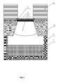
- the object of the invention is a method for the production of long monocrystals of silicon carbide with the use of a furnace for SiC monocrystallization, the furnace comprising two heaters, i.e. an upper heater which serves as a main heater and a lower heater which serves as an additional heater ( Fig. 1 ). Inside the upper heater, there is a growth chamber, and the lower heater is located under the upper heater. It heats the growth chamber from the bottom. With this method, the temperature difference between the source material and the surface of the crystal growth can be increased. Furthermore, with the additional heater, the shape of the crystallization front during the crystal growth can be controlled to a certain extent. This solution allows a high yield of the crystallization process by increasing the length of the obtained crystals.
- a method of producing silicon carbide crystals in a device comprising an upper heater, a lower heater, located beneath the upper heater, and a growth chamber, located inside the upper heater, provided with a crucible for a source material and a crucible cover allowing fixing of a monocrystalline seed thereon, wherein the monocrystalline seed is placed in an upper part of the growth chamber, and the source material is placed in the crucible, the growth chamber is filled with an inert gas, by means of the upper and lower heaters, the monocrystalline seed is heated to a temperature of at least 2150°C, and the source material to a higher temperature, preferably at least 2300°C, during the process, the source material is maintained at a higher temperature than the seed, and in these conditions, thermal decomposition of the source material and crystallization of silicon carbide on the monocrystalline seed are performed to give a silicon carbide crystal, is characterised in that during the crystallization of silicon carbide on the monocrystalline seed, power Pg supplied to the upper heater and power P d
- the rear surface of the monocrystalline seed i.e. the surface which, in the growth process, faces outward relative to the crucible, is covered preferably with a graphite plate during the crystallization of silicon carbide on the monocrystalline seed
- step b) power P g supplied to the upper heater is gradually reduced over time.
- the rear surface of the monocrystalline seed i.e. the surface which, in the growth process, faces outward relative to the crucible, is left uncovered during the crystallization of silicon carbide on the monocrystalline seed
- step e power P g supplied to the upper heater is gradually increased over time.
- step c) or f) power P d supplied to the lower heater is gradually increased over time.
- a seed in the form of a plate with only one front surface polished is used.
- a seed crystallographically oriented along a direction consistent with crystallographic axis c is used.
- a seed in the form of a plate having a thickness of 1-2 mm is used.
- a 4H-SiC plate is used, preferably the one the growth surface, i.e. the surface which in the growth process faces inward relative to the crucible, of which has carbon polarity.
- a 6H-SiC plate is used, preferably the one the growth surface, i.e. the surface which in the growth process faces inward relative to the crucible, of which has silicon polarity.
- silicon carbide possibly doped with boron, vanadium or aluminum, or silicon carbide of a non-stoichiometric composition, containing an excess of silicon or carbon, is used.
- the inert gas contains nitrogen or the inert gas is nitrogen
- the seed is heated to a temperature of 2000-2300°C on its rear surface.
- the process is carried out using a temperature field and a field of partial pressures of vapours from which a crystal is formed, adapted to the speed of the crystal growth in the range of 0.01-2 mm/h.
- the method according to the invention - in the most general terms - consists in that the temperature field in the growth chamber during the crystallization process is modified as a function of crystal length. In such a manner that the power supplied to the lower and upper heaters is modified smoothly depending on the length of the crystal being obtained.
- the invention is used for two methods of fixing the monocrystalline seed.
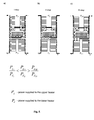
- the seed is adhered to a graphite plate, and its rear surface is completely covered ( Fig. 2 ).
- a plate is fixed on the edge of the inner opening of the crucible cover, and its rear surface is completely uncovered ( Fig. 3 ).
- the method of heating in the first phase of the crystal growth will vary depending on the method of fixing the seed. In the later part of the crystallization process, in both cases, the method of heating will be similar.
- the rear surface of the seed when the rear surface of the seed is covered e.g. with a graphite plate, it is preferable to form a substantial radial gradient on the growth surface of seed in the first phase of the crystal growth - this will allow growth of the crystal with a convex growth surface, and more importantly, will reduce the phenomenon of formation of many crystallization nuclei. It is intended to have, at the top of the convex crystallization front, just one source of crystallization degrees, from which crystallization degrees will propagate uniformly from the centre to the edge of the crystal. This allows for stabilisation of polytype, degree of doping and improves the stability of the growth surface morphology.
- Convexity of the crystallization front can not be too large because internal stresses will be created in the crystal and there will be a risk of crystallization steps being grouped.
- the crystallization front is intended to be characterised by a small convexity. Convexity is measured with an inclination angle between a tangent drawn at the growth surface to a tangent to the seed surface at the crystal edge. The optimal size of this angle is equal to ⁇ ⁇ 3.5°.
- the largest radial gradient is obtained when the largest ratio of P g P d is maintained, i.e. when the highest possible power is supplied to the upper heater, and the lowest power to the lower one.
- value P g P d is reduced in a smooth manner. While maintaining the radial gradient which allows the growth of the crystal with a convex crystallization front, where angle ⁇ ⁇ 3. 5°. With the increase in the length of the crystal, heat flow through the crystal is becoming more difficult, which causes a temperature rise on the surface of the crystal growth. In these conditions, crystallization rate decreases and the crystallization front becomes flat, and even concave.
- Possibility of growth of longer crystals preferably reduces the cost of the process. From the obtained crystals, a larger amount of plates, which are substrates for the production of electronic devices, is preferably obtained. From one seed, a larger amount of plates is preferably obtained, which lowers the cost of production of the obtained substrates.
- Crystal growth processes consist of many steps, i.e. preparation of the system, obtaining a vacuum in the furnace chamber, then heating the growth chamber to the temperature of crystallization and cooling the growth chamber and its unloading. By obtaining longer crystals, the impact of steps in which crystal growth does not take place on the process efficiency is reduced. Furthermore, in the process of obtaining plates from the crystal, it has preferably a greater length because this allows for better efficiency when it is being cut into plates.
- a monocrystalline seed in the form of a SiC plate with a polished surface on which the crystal growth will take place is preferably used.
- organic adhesives or a graphite paste are preferably used.
- the plate with an uncovered rear surface the plate is preferably fixed with its edge on an annular shoulder constituting an integral part of the crucible cover. If necessary, the seed edge is sealed preferably by means of a graphite paste and is covered with an additional graphite ring.
- Preparation of the seed in this method is preferably limited to polishing of only one front surface of the plate without the need to maintain the flatness of the rear surface of the plate, which results in a considerable time saving.
- the seed in the plane (0001) crystallographically oriented along a direction consistent with crystallographic axis c is commonly used, but is also possible to use seeds with other crystallographic orientations.
- carbon surface of the seed is preferably used, and for 6H-SiC crystal growth, silicon surface of the seed is preferably used.
- the used seed in the form of a plate preferably has a thickness of 1-2 mm.
- silicon carbide is preferably used, which, depending on the intended properties of the obtained crystal, is used without dopants or is intentionally enriched with dopants, such as boron, vanadium, cerium, aluminum, iron and/or excessive stoichiometric silicon or carbon, SiC source material has preferably the form of powder, granulate or recrystallised SiC material.
- the gas which fills the growth chamber typically argon, nitrogen, hydrogen and/or helium are used.
- silicon carbide as the source material, is placed in the growth chamber filled with nitrogen or with an inert gas containing nitrogen.
- the seed is preferably heated to a temperature of 2000-2300 °C, on its rear surface, and the source material to a temperature of 2100-2400 °C.
- the process is carried out using a temperature field and a field of partial pressures of vapours from which a crystal is formed, adapted to the speed of crystal growth preferably in the range of 0.01-2 mm/h.
- the method according to the invention provides a high reproducibility of long 4H- and 6H-SiC crystals of the same polytype.
- the invention also allows a controlled and homogeneous doping which allows production of crystals with a wide range of electrical and optical properties. This also allows the use of a nonconventional direction of crystallization.
- a growth chamber 1 is placed inside an upper heater 2 ( Fig. 1 ).
- a lower heater 3 is located below the upper heater 2 and heats its bottom from below.
- the growth chamber 1 includes a graphite crucible 9 ( Fig. 2 ) in which a source material 7 ( Fig. 2 ) and a crucible cover 10 ( Fig. 2 ) are located, a monocrystalline 4H-SiC seed 6 with orientation (000-1) ( Fig. 2 ) being fixed to the said crucible cover so that its rear surface is covered with a graphite plate 11.
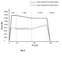
- the seed 6 is heated to a temperature of 2250 °C, and the source material 7 to a temperature of 2300 °C.
- a constant power is supplied in an amount of 16000W to the upper heater 2 and 8000W to the lower heater 3 for 30 hours.
- the amount of power supplied to the upper heater 2 is reduced by 1000W, and the power supplied to the lower heater 3 is controlled until reaching a temperature of 2200 °C measured on crystal 8, while maintaining a temperature of 2300 °C of the source material 7.
- the power supplied to the lower heater 3 is increased until reaching a temperature of 2400 °C measured for the source material 7.
- the growth chamber 1 during the crystallization is filled with argon at a pressure of 2 kPa.
- the growth chamber 1 was placed as in Example 1 except that the rear surface of the seed 6 is uncovered ( Fig. 3 ).
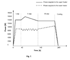
- the seed 6 is heated to a temperature of 2150 °C, and the source material 7 to a temperature of 2300 °C. Then, a constant power is supplied in an amount of 14000 W to the upper heater 2 and 9000W to the lower heater 3 for 30 hours.
- a constant power is supplied in an amount of 14000 W to the upper heater 2 and 9000W to the lower heater 3 for 30 hours.
- Fig. 5a and 7 the first phase of the process
- the source material 7 to a temperature of 2300 °C.
- a constant power is supplied in an amount of 14000 W to the upper heater 2 and 9000W to the lower heater 3 for 30 hours.
- the second phase of the process Fig.
- the heating power for the upper heater 2 is smoothly increased by 2000W for 30 hours, and the power supplied to the lower heater 3 is controlled, then for 70 hours, the power supplied to the upper heater 2 is smoothly reduced until reaching a temperature of 2200 °C measured on the crystal 8, while maintaining a temperature of 2300 °C of the source material 7.
- the heating power for the lower heater 3 is increased until reaching a temperature of 2400 °C measured for the source material 7.
- the growth chamber 1 during the crystallization is filled with argon at a pressure of 2 kPa.
- Example 3 growth on silicon polarity - 6H-SiC crystal
- the growth chamber 1 was placed as in Example 1 except that the polarity of the seed 6 was changed to silicon one (0001). Other crystallization conditions were also as in Example 1.
- the growth chamber 1 ( Fig. 1 ) and the seed 6 ( Fig. 2 ) were placed as in Example 1.
- a mixture of argon and nitrogen in a ratio of 90:10 at a pressure of 2 kPa was used as an atmosphere of growth.
- Thermal conditions were the same as in Example 1.
- Example 5 nitrogen doping, growth on silicon polarity
- the growth chamber 1 ( Fig. 1 ) was placed as in Example 1, and the seed 6 as in Example 3.
- a mixture of argon and nitrogen in a ratio of 90:10 at a pressure of 2 kPa was used as an atmosphere of growth.
- Thermal conditions were the same as in Example 1.
- the growth chamber 1 ( Fig. 1 ) was placed as in Example 1, and the seed 6 as in Example 3.
- the source material 7 in the form of silicon carbide powder doped with boron was placed.
- Other crystallization conditions were also as in Example 1.
- the growth chamber 1 ( Fig. 1 ) and the seed 6 ( Fig. 2 ) were placed as in Example 1.
- the source material 7 in the form of recrystallised silicon carbide doped with vanadium was placed.
- Other crystallization conditions were also as in Example 1.
Landscapes
- Chemical & Material Sciences (AREA)
- Engineering & Computer Science (AREA)
- Crystallography & Structural Chemistry (AREA)
- Materials Engineering (AREA)
- Metallurgy (AREA)
- Organic Chemistry (AREA)
- Inorganic Chemistry (AREA)
- Crystals, And After-Treatments Of Crystals (AREA)
Applications Claiming Priority (1)
| Application Number | Priority Date | Filing Date | Title |
|---|---|---|---|
| PL411695A PL238539B1 (pl) | 2015-03-25 | 2015-03-25 | Sposób wytwarzania kryształów węglika krzemu |
Publications (2)
| Publication Number | Publication Date |
|---|---|
| EP3072995A1 true EP3072995A1 (de) | 2016-09-28 |
| EP3072995B1 EP3072995B1 (de) | 2020-05-06 |
Family
ID=53191453
Family Applications (1)
| Application Number | Title | Priority Date | Filing Date |
|---|---|---|---|
| EP15161654.7A Not-in-force EP3072995B1 (de) | 2015-03-25 | 2015-03-30 | Verfahren zur kristallenzüchtung von siliziumkarbid mittels verdampfung |
Country Status (2)
| Country | Link |
|---|---|
| EP (1) | EP3072995B1 (de) |
| PL (1) | PL238539B1 (de) |
Cited By (3)
| Publication number | Priority date | Publication date | Assignee | Title |
|---|---|---|---|---|
| CN111621844A (zh) * | 2020-06-22 | 2020-09-04 | 哈尔滨化兴软控科技有限公司 | 一种旋转式双温区pvt法高质量单晶制备装置及方法 |
| EP3767014A4 (de) * | 2018-03-15 | 2021-12-01 | Shin-Etsu Handotai Co., Ltd. | Verfahren zur herstellung eines siliciumcarbideinkristalls |
| CN113862789A (zh) * | 2021-12-01 | 2021-12-31 | 浙江大学杭州国际科创中心 | 一种制备p型4H-SiC单晶的坩埚结构与装置与方法 |
Citations (5)
| Publication number | Priority date | Publication date | Assignee | Title |
|---|---|---|---|---|
| EP1354987A1 (de) * | 2000-12-28 | 2003-10-22 | Bridgestone Corporation | Siliciumcarbid-einkristall und verfahren und vorrichtung zu seiner herstellung |
| WO2007135965A1 (en) * | 2006-05-18 | 2007-11-29 | Showa Denko K.K. | Method for producing silicon carbide single crystal |
| JP2007314358A (ja) * | 2006-05-23 | 2007-12-06 | Bridgestone Corp | 炭化ケイ素単結晶の製造装置及びその製造方法 |
| US20100139552A1 (en) * | 2008-12-08 | 2010-06-10 | Ii-Iv Incorporated | Axial Gradient Transport Growth Process and Apparatus Utilizing Resistive Heating |
| EP2371997A1 (de) * | 2010-04-01 | 2011-10-05 | Instytut Technologii Materialów Elektronicznych | Verfahren zur Herstellung von Kristallen, insbesondere Siliciumcarbid, aus der gasförmigen Phase |
-
2015
- 2015-03-25 PL PL411695A patent/PL238539B1/pl unknown
- 2015-03-30 EP EP15161654.7A patent/EP3072995B1/de not_active Not-in-force
Patent Citations (5)
| Publication number | Priority date | Publication date | Assignee | Title |
|---|---|---|---|---|
| EP1354987A1 (de) * | 2000-12-28 | 2003-10-22 | Bridgestone Corporation | Siliciumcarbid-einkristall und verfahren und vorrichtung zu seiner herstellung |
| WO2007135965A1 (en) * | 2006-05-18 | 2007-11-29 | Showa Denko K.K. | Method for producing silicon carbide single crystal |
| JP2007314358A (ja) * | 2006-05-23 | 2007-12-06 | Bridgestone Corp | 炭化ケイ素単結晶の製造装置及びその製造方法 |
| US20100139552A1 (en) * | 2008-12-08 | 2010-06-10 | Ii-Iv Incorporated | Axial Gradient Transport Growth Process and Apparatus Utilizing Resistive Heating |
| EP2371997A1 (de) * | 2010-04-01 | 2011-10-05 | Instytut Technologii Materialów Elektronicznych | Verfahren zur Herstellung von Kristallen, insbesondere Siliciumcarbid, aus der gasförmigen Phase |
Non-Patent Citations (6)
| Title |
|---|
| 0. KORDINA; C. HALLIN; A. ELLISON; A. S. BAKIN; I. G. IVANOV; A. HENRY; R. YAKIMOVA; M. TOUMINEN; A. VEHANEN; E. JANZEN, APPL. PHYS. LETT., vol. 69, 1996, pages 1456 |
| A. J. LELY, BER. DEUT. KERAM. GES., vol. 32, 1955, pages 229 |
| KRZYSZTOF GRASZA ET AL: "Experimental Verification of a Novel System for the Growth of SiC Single Crystals", MATERIALS SCIENCE FORUM, vol. 679-680, 28 March 2011 (2011-03-28), CH, pages 16 - 19, XP055295132, ISSN: 0255-5476, DOI: 10.4028/www.scientific.net/MSF.679-680.16 * |
| T. UJIHARA; R. MAEKAWA; R. TANAKA; K. SASAKI; K. KURODAB; Y. TAKEDA, J. CRYST. GROWTH, vol. 310, 2008, pages 1438 |
| T.S SUDARSHAN; S. I. MAXIMENKO, MICROELECTRONIC ENGINEERING, vol. 83, 2006, pages 155 - 159 |
| Y.M.TAIROV; V.F.TSVETKOW, J.CRYSTAL GROWTH, vol. 43, 1978, pages 209 |
Cited By (4)
| Publication number | Priority date | Publication date | Assignee | Title |
|---|---|---|---|---|
| EP3767014A4 (de) * | 2018-03-15 | 2021-12-01 | Shin-Etsu Handotai Co., Ltd. | Verfahren zur herstellung eines siliciumcarbideinkristalls |
| CN111621844A (zh) * | 2020-06-22 | 2020-09-04 | 哈尔滨化兴软控科技有限公司 | 一种旋转式双温区pvt法高质量单晶制备装置及方法 |
| CN113862789A (zh) * | 2021-12-01 | 2021-12-31 | 浙江大学杭州国际科创中心 | 一种制备p型4H-SiC单晶的坩埚结构与装置与方法 |
| CN113862789B (zh) * | 2021-12-01 | 2022-03-11 | 浙江大学杭州国际科创中心 | 一种制备p型4H-SiC单晶的坩埚结构与装置与方法 |
Also Published As
| Publication number | Publication date |
|---|---|
| PL411695A1 (pl) | 2016-09-26 |
| PL238539B1 (pl) | 2021-09-06 |
| EP3072995B1 (de) | 2020-05-06 |
Similar Documents
| Publication | Publication Date | Title |
|---|---|---|
| US9893152B2 (en) | Semi-insulating silicon carbide monocrystal and method of growing the same | |
| US9068277B2 (en) | Apparatus for manufacturing single-crystal silicon carbide | |
| JP5483216B2 (ja) | SiC単結晶およびその製造方法 | |
| KR100773624B1 (ko) | 탄화 규소 단결정으로 이루어지는 종결정 및 그를 이용한잉곳의 제조 방법 | |
| CN101724893B (zh) | 一种制备高纯半绝缘碳化硅晶体的方法 | |
| JP2008504203A (ja) | 100ミリメートル高純度半絶縁単結晶炭化珪素ウエハ | |
| CN103696012B (zh) | 一种高均匀性、高产率半绝缘碳化硅衬底的制备方法 | |
| PL234396B1 (pl) | Sposób wytwarzania kryształów, zwłaszcza węglika krzemu, z fazy gazowej | |
| CN108118394B (zh) | 一种降低碳化硅单晶中氮杂质含量的方法 | |
| JP2008001532A (ja) | 炭化珪素単結晶インゴット及びその製造方法 | |
| JP2004099340A (ja) | 炭化珪素単結晶育成用種結晶と炭化珪素単結晶インゴット及びその製造方法 | |
| Chaussende et al. | Status of SiC bulk growth processes | |
| EP3072995B1 (de) | Verfahren zur kristallenzüchtung von siliziumkarbid mittels verdampfung | |
| CN105568385A (zh) | 一种掺锗SiC体单晶材料的生长方法 | |
| KR101767295B1 (ko) | 단결정 탄화규소 액상 에피택셜 성장용 시드재 및 단결정 탄화규소의 액상 에피택셜 성장 방법 | |
| JP3508519B2 (ja) | エピタキシャル成長装置およびエピタキシャル成長法 | |
| JP3590464B2 (ja) | 4h型単結晶炭化珪素の製造方法 | |
| JP5761264B2 (ja) | SiC基板の製造方法 | |
| JP2018168052A (ja) | 炭化珪素単結晶インゴットの製造方法 | |
| JP2002293694A (ja) | 炭化珪素単結晶インゴット及びその製造方法 | |
| JP2017154953A (ja) | 炭化珪素単結晶製造装置 | |
| JP2003137694A (ja) | 炭化珪素単結晶育成用種結晶と炭化珪素単結晶インゴット及びその製造方法 | |
| JP2011201756A (ja) | 単結晶炭化珪素の製造方法 | |
| JP4446464B2 (ja) | 炭化珪素単結晶のエピタキシャル成長方法 | |
| JPH09142995A (ja) | P型単結晶炭化珪素の製造方法 |
Legal Events
| Date | Code | Title | Description |
|---|---|---|---|
| PUAI | Public reference made under article 153(3) epc to a published international application that has entered the european phase |
Free format text: ORIGINAL CODE: 0009012 |
|
| AK | Designated contracting states |
Kind code of ref document: A1 Designated state(s): AL AT BE BG CH CY CZ DE DK EE ES FI FR GB GR HR HU IE IS IT LI LT LU LV MC MK MT NL NO PL PT RO RS SE SI SK SM TR |
|
| AX | Request for extension of the european patent |
Extension state: BA ME |
|
| STAA | Information on the status of an ep patent application or granted ep patent |
Free format text: STATUS: REQUEST FOR EXAMINATION WAS MADE |
|
| 17P | Request for examination filed |
Effective date: 20170327 |
|
| RBV | Designated contracting states (corrected) |
Designated state(s): AL AT BE BG CH CY CZ DE DK EE ES FI FR GB GR HR HU IE IS IT LI LT LU LV MC MK MT NL NO PL PT RO RS SE SI SK SM TR |
|
| STAA | Information on the status of an ep patent application or granted ep patent |
Free format text: STATUS: EXAMINATION IS IN PROGRESS |
|
| 17Q | First examination report despatched |
Effective date: 20190415 |
|
| GRAP | Despatch of communication of intention to grant a patent |
Free format text: ORIGINAL CODE: EPIDOSNIGR1 |
|
| STAA | Information on the status of an ep patent application or granted ep patent |
Free format text: STATUS: GRANT OF PATENT IS INTENDED |
|
| INTG | Intention to grant announced |
Effective date: 20190920 |
|
| GRAS | Grant fee paid |
Free format text: ORIGINAL CODE: EPIDOSNIGR3 |
|
| RAP1 | Party data changed (applicant data changed or rights of an application transferred) |
Owner name: SIEC BADAWCZA LUKASIEWICZ- INSTYTUT TECHNOLOGII MATERIALOW ELEKTRONICZNYCH |
|
| GRAA | (expected) grant |
Free format text: ORIGINAL CODE: 0009210 |
|
| STAA | Information on the status of an ep patent application or granted ep patent |
Free format text: STATUS: THE PATENT HAS BEEN GRANTED |
|
| AK | Designated contracting states |
Kind code of ref document: B1 Designated state(s): AL AT BE BG CH CY CZ DE DK EE ES FI FR GB GR HR HU IE IS IT LI LT LU LV MC MK MT NL NO PL PT RO RS SE SI SK SM TR |
|
| REG | Reference to a national code |
Ref country code: GB Ref legal event code: FG4D |
|
| REG | Reference to a national code |
Ref country code: CH Ref legal event code: EP Ref country code: AT Ref legal event code: REF Ref document number: 1266874 Country of ref document: AT Kind code of ref document: T Effective date: 20200515 |
|
| REG | Reference to a national code |
Ref country code: IE Ref legal event code: FG4D |
|
| REG | Reference to a national code |
Ref country code: DE Ref legal event code: R096 Ref document number: 602015051997 Country of ref document: DE |
|
| REG | Reference to a national code |
Ref country code: LT Ref legal event code: MG4D |
|
| REG | Reference to a national code |
Ref country code: NL Ref legal event code: MP Effective date: 20200506 |
|
| PG25 | Lapsed in a contracting state [announced via postgrant information from national office to epo] |
Ref country code: SE Free format text: LAPSE BECAUSE OF FAILURE TO SUBMIT A TRANSLATION OF THE DESCRIPTION OR TO PAY THE FEE WITHIN THE PRESCRIBED TIME-LIMIT Effective date: 20200506 Ref country code: PT Free format text: LAPSE BECAUSE OF FAILURE TO SUBMIT A TRANSLATION OF THE DESCRIPTION OR TO PAY THE FEE WITHIN THE PRESCRIBED TIME-LIMIT Effective date: 20200907 Ref country code: FI Free format text: LAPSE BECAUSE OF FAILURE TO SUBMIT A TRANSLATION OF THE DESCRIPTION OR TO PAY THE FEE WITHIN THE PRESCRIBED TIME-LIMIT Effective date: 20200506 Ref country code: IS Free format text: LAPSE BECAUSE OF FAILURE TO SUBMIT A TRANSLATION OF THE DESCRIPTION OR TO PAY THE FEE WITHIN THE PRESCRIBED TIME-LIMIT Effective date: 20200906 Ref country code: NO Free format text: LAPSE BECAUSE OF FAILURE TO SUBMIT A TRANSLATION OF THE DESCRIPTION OR TO PAY THE FEE WITHIN THE PRESCRIBED TIME-LIMIT Effective date: 20200806 Ref country code: GR Free format text: LAPSE BECAUSE OF FAILURE TO SUBMIT A TRANSLATION OF THE DESCRIPTION OR TO PAY THE FEE WITHIN THE PRESCRIBED TIME-LIMIT Effective date: 20200807 Ref country code: LT Free format text: LAPSE BECAUSE OF FAILURE TO SUBMIT A TRANSLATION OF THE DESCRIPTION OR TO PAY THE FEE WITHIN THE PRESCRIBED TIME-LIMIT Effective date: 20200506 |
|
| PG25 | Lapsed in a contracting state [announced via postgrant information from national office to epo] |
Ref country code: LV Free format text: LAPSE BECAUSE OF FAILURE TO SUBMIT A TRANSLATION OF THE DESCRIPTION OR TO PAY THE FEE WITHIN THE PRESCRIBED TIME-LIMIT Effective date: 20200506 Ref country code: BG Free format text: LAPSE BECAUSE OF FAILURE TO SUBMIT A TRANSLATION OF THE DESCRIPTION OR TO PAY THE FEE WITHIN THE PRESCRIBED TIME-LIMIT Effective date: 20200806 Ref country code: RS Free format text: LAPSE BECAUSE OF FAILURE TO SUBMIT A TRANSLATION OF THE DESCRIPTION OR TO PAY THE FEE WITHIN THE PRESCRIBED TIME-LIMIT Effective date: 20200506 Ref country code: HR Free format text: LAPSE BECAUSE OF FAILURE TO SUBMIT A TRANSLATION OF THE DESCRIPTION OR TO PAY THE FEE WITHIN THE PRESCRIBED TIME-LIMIT Effective date: 20200506 |
|
| REG | Reference to a national code |
Ref country code: AT Ref legal event code: MK05 Ref document number: 1266874 Country of ref document: AT Kind code of ref document: T Effective date: 20200506 |
|
| PG25 | Lapsed in a contracting state [announced via postgrant information from national office to epo] |
Ref country code: NL Free format text: LAPSE BECAUSE OF FAILURE TO SUBMIT A TRANSLATION OF THE DESCRIPTION OR TO PAY THE FEE WITHIN THE PRESCRIBED TIME-LIMIT Effective date: 20200506 Ref country code: AL Free format text: LAPSE BECAUSE OF FAILURE TO SUBMIT A TRANSLATION OF THE DESCRIPTION OR TO PAY THE FEE WITHIN THE PRESCRIBED TIME-LIMIT Effective date: 20200506 |
|
| PG25 | Lapsed in a contracting state [announced via postgrant information from national office to epo] |
Ref country code: RO Free format text: LAPSE BECAUSE OF FAILURE TO SUBMIT A TRANSLATION OF THE DESCRIPTION OR TO PAY THE FEE WITHIN THE PRESCRIBED TIME-LIMIT Effective date: 20200506 Ref country code: EE Free format text: LAPSE BECAUSE OF FAILURE TO SUBMIT A TRANSLATION OF THE DESCRIPTION OR TO PAY THE FEE WITHIN THE PRESCRIBED TIME-LIMIT Effective date: 20200506 Ref country code: AT Free format text: LAPSE BECAUSE OF FAILURE TO SUBMIT A TRANSLATION OF THE DESCRIPTION OR TO PAY THE FEE WITHIN THE PRESCRIBED TIME-LIMIT Effective date: 20200506 Ref country code: IT Free format text: LAPSE BECAUSE OF FAILURE TO SUBMIT A TRANSLATION OF THE DESCRIPTION OR TO PAY THE FEE WITHIN THE PRESCRIBED TIME-LIMIT Effective date: 20200506 Ref country code: SM Free format text: LAPSE BECAUSE OF FAILURE TO SUBMIT A TRANSLATION OF THE DESCRIPTION OR TO PAY THE FEE WITHIN THE PRESCRIBED TIME-LIMIT Effective date: 20200506 Ref country code: DK Free format text: LAPSE BECAUSE OF FAILURE TO SUBMIT A TRANSLATION OF THE DESCRIPTION OR TO PAY THE FEE WITHIN THE PRESCRIBED TIME-LIMIT Effective date: 20200506 Ref country code: ES Free format text: LAPSE BECAUSE OF FAILURE TO SUBMIT A TRANSLATION OF THE DESCRIPTION OR TO PAY THE FEE WITHIN THE PRESCRIBED TIME-LIMIT Effective date: 20200506 Ref country code: CZ Free format text: LAPSE BECAUSE OF FAILURE TO SUBMIT A TRANSLATION OF THE DESCRIPTION OR TO PAY THE FEE WITHIN THE PRESCRIBED TIME-LIMIT Effective date: 20200506 |
|
| REG | Reference to a national code |
Ref country code: DE Ref legal event code: R097 Ref document number: 602015051997 Country of ref document: DE |
|
| PG25 | Lapsed in a contracting state [announced via postgrant information from national office to epo] |
Ref country code: SK Free format text: LAPSE BECAUSE OF FAILURE TO SUBMIT A TRANSLATION OF THE DESCRIPTION OR TO PAY THE FEE WITHIN THE PRESCRIBED TIME-LIMIT Effective date: 20200506 Ref country code: PL Free format text: LAPSE BECAUSE OF FAILURE TO SUBMIT A TRANSLATION OF THE DESCRIPTION OR TO PAY THE FEE WITHIN THE PRESCRIBED TIME-LIMIT Effective date: 20200506 |
|
| PLBE | No opposition filed within time limit |
Free format text: ORIGINAL CODE: 0009261 |
|
| STAA | Information on the status of an ep patent application or granted ep patent |
Free format text: STATUS: NO OPPOSITION FILED WITHIN TIME LIMIT |
|
| 26N | No opposition filed |
Effective date: 20210209 |
|
| PG25 | Lapsed in a contracting state [announced via postgrant information from national office to epo] |
Ref country code: SI Free format text: LAPSE BECAUSE OF FAILURE TO SUBMIT A TRANSLATION OF THE DESCRIPTION OR TO PAY THE FEE WITHIN THE PRESCRIBED TIME-LIMIT Effective date: 20200506 |
|
| PG25 | Lapsed in a contracting state [announced via postgrant information from national office to epo] |
Ref country code: MC Free format text: LAPSE BECAUSE OF FAILURE TO SUBMIT A TRANSLATION OF THE DESCRIPTION OR TO PAY THE FEE WITHIN THE PRESCRIBED TIME-LIMIT Effective date: 20200506 |
|
| REG | Reference to a national code |
Ref country code: CH Ref legal event code: PL |
|
| GBPC | Gb: european patent ceased through non-payment of renewal fee |
Effective date: 20210330 |
|
| REG | Reference to a national code |
Ref country code: BE Ref legal event code: MM Effective date: 20210331 |
|
| PG25 | Lapsed in a contracting state [announced via postgrant information from national office to epo] |
Ref country code: GB Free format text: LAPSE BECAUSE OF NON-PAYMENT OF DUE FEES Effective date: 20210330 Ref country code: IE Free format text: LAPSE BECAUSE OF NON-PAYMENT OF DUE FEES Effective date: 20210330 Ref country code: FR Free format text: LAPSE BECAUSE OF NON-PAYMENT OF DUE FEES Effective date: 20210331 Ref country code: CH Free format text: LAPSE BECAUSE OF NON-PAYMENT OF DUE FEES Effective date: 20210331 Ref country code: LU Free format text: LAPSE BECAUSE OF NON-PAYMENT OF DUE FEES Effective date: 20210330 Ref country code: LI Free format text: LAPSE BECAUSE OF NON-PAYMENT OF DUE FEES Effective date: 20210331 |
|
| PG25 | Lapsed in a contracting state [announced via postgrant information from national office to epo] |
Ref country code: BE Free format text: LAPSE BECAUSE OF NON-PAYMENT OF DUE FEES Effective date: 20210331 |
|
| PG25 | Lapsed in a contracting state [announced via postgrant information from national office to epo] |
Ref country code: HU Free format text: LAPSE BECAUSE OF FAILURE TO SUBMIT A TRANSLATION OF THE DESCRIPTION OR TO PAY THE FEE WITHIN THE PRESCRIBED TIME-LIMIT; INVALID AB INITIO Effective date: 20150330 |
|
| PGFP | Annual fee paid to national office [announced via postgrant information from national office to epo] |
Ref country code: DE Payment date: 20230327 Year of fee payment: 9 |
|
| PG25 | Lapsed in a contracting state [announced via postgrant information from national office to epo] |
Ref country code: CY Free format text: LAPSE BECAUSE OF FAILURE TO SUBMIT A TRANSLATION OF THE DESCRIPTION OR TO PAY THE FEE WITHIN THE PRESCRIBED TIME-LIMIT Effective date: 20200506 |
|
| PG25 | Lapsed in a contracting state [announced via postgrant information from national office to epo] |
Ref country code: MK Free format text: LAPSE BECAUSE OF FAILURE TO SUBMIT A TRANSLATION OF THE DESCRIPTION OR TO PAY THE FEE WITHIN THE PRESCRIBED TIME-LIMIT Effective date: 20200506 |
|
| PG25 | Lapsed in a contracting state [announced via postgrant information from national office to epo] |
Ref country code: MT Free format text: LAPSE BECAUSE OF FAILURE TO SUBMIT A TRANSLATION OF THE DESCRIPTION OR TO PAY THE FEE WITHIN THE PRESCRIBED TIME-LIMIT Effective date: 20200506 |
|
| REG | Reference to a national code |
Ref country code: DE Ref legal event code: R119 Ref document number: 602015051997 Country of ref document: DE |
|
| PG25 | Lapsed in a contracting state [announced via postgrant information from national office to epo] |
Ref country code: DE Free format text: LAPSE BECAUSE OF NON-PAYMENT OF DUE FEES Effective date: 20241001 |
|
| PG25 | Lapsed in a contracting state [announced via postgrant information from national office to epo] |
Ref country code: DE Free format text: LAPSE BECAUSE OF NON-PAYMENT OF DUE FEES Effective date: 20241001 |
|
| PG25 | Lapsed in a contracting state [announced via postgrant information from national office to epo] |
Ref country code: TR Free format text: LAPSE BECAUSE OF FAILURE TO SUBMIT A TRANSLATION OF THE DESCRIPTION OR TO PAY THE FEE WITHIN THE PRESCRIBED TIME-LIMIT Effective date: 20200506 |