EP3073636A2 - Solarzellenmodul und verfahren zur herstellung davon - Google Patents
Solarzellenmodul und verfahren zur herstellung davon Download PDFInfo
- Publication number
- EP3073636A2 EP3073636A2 EP15165204.7A EP15165204A EP3073636A2 EP 3073636 A2 EP3073636 A2 EP 3073636A2 EP 15165204 A EP15165204 A EP 15165204A EP 3073636 A2 EP3073636 A2 EP 3073636A2
- Authority
- EP
- European Patent Office
- Prior art keywords
- solar panel
- solar
- solar panels
- back sheet
- encapsulant
- Prior art date
- Legal status (The legal status is an assumption and is not a legal conclusion. Google has not performed a legal analysis and makes no representation as to the accuracy of the status listed.)
- Withdrawn
Links
- 238000000034 method Methods 0.000 title claims description 17
- 239000008393 encapsulating agent Substances 0.000 claims description 45
- 239000000565 sealant Substances 0.000 claims description 23
- XLYOFNOQVPJJNP-UHFFFAOYSA-N water Substances O XLYOFNOQVPJJNP-UHFFFAOYSA-N 0.000 claims description 18
- 238000006243 chemical reaction Methods 0.000 claims description 14
- 229920000098 polyolefin Polymers 0.000 claims description 11
- 229920002037 poly(vinyl butyral) polymer Polymers 0.000 claims description 8
- 239000011521 glass Substances 0.000 claims description 6
- 239000005038 ethylene vinyl acetate Substances 0.000 claims description 4
- 238000010030 laminating Methods 0.000 claims description 3
- NIXOWILDQLNWCW-UHFFFAOYSA-N acrylic acid group Chemical group C(C=C)(=O)O NIXOWILDQLNWCW-UHFFFAOYSA-N 0.000 claims description 2
- 229920005549 butyl rubber Polymers 0.000 claims description 2
- 239000000463 material Substances 0.000 description 7
- 239000010949 copper Substances 0.000 description 5
- RYGMFSIKBFXOCR-UHFFFAOYSA-N Copper Chemical compound [Cu] RYGMFSIKBFXOCR-UHFFFAOYSA-N 0.000 description 4
- 239000011669 selenium Substances 0.000 description 4
- 238000000926 separation method Methods 0.000 description 4
- 229910052802 copper Inorganic materials 0.000 description 3
- 229920005989 resin Polymers 0.000 description 3
- 239000011347 resin Substances 0.000 description 3
- GYHNNYVSQQEPJS-UHFFFAOYSA-N Gallium Chemical compound [Ga] GYHNNYVSQQEPJS-UHFFFAOYSA-N 0.000 description 2
- 239000004952 Polyamide Substances 0.000 description 2
- 239000004698 Polyethylene Substances 0.000 description 2
- BUGBHKTXTAQXES-UHFFFAOYSA-N Selenium Chemical compound [Se] BUGBHKTXTAQXES-UHFFFAOYSA-N 0.000 description 2
- 239000000853 adhesive Substances 0.000 description 2
- 230000001070 adhesive effect Effects 0.000 description 2
- 229910045601 alloy Inorganic materials 0.000 description 2
- 239000000956 alloy Substances 0.000 description 2
- 239000003989 dielectric material Substances 0.000 description 2
- 230000005611 electricity Effects 0.000 description 2
- 239000011888 foil Substances 0.000 description 2
- 229910052733 gallium Inorganic materials 0.000 description 2
- 229910052738 indium Inorganic materials 0.000 description 2
- APFVFJFRJDLVQX-UHFFFAOYSA-N indium atom Chemical compound [In] APFVFJFRJDLVQX-UHFFFAOYSA-N 0.000 description 2
- 229910052751 metal Inorganic materials 0.000 description 2
- 239000002184 metal Substances 0.000 description 2
- 150000002739 metals Chemical class 0.000 description 2
- 238000012986 modification Methods 0.000 description 2
- 230000004048 modification Effects 0.000 description 2
- 229920002647 polyamide Polymers 0.000 description 2
- -1 polyethylene Polymers 0.000 description 2
- 229920000573 polyethylene Polymers 0.000 description 2
- 229920000139 polyethylene terephthalate Polymers 0.000 description 2
- 239000005020 polyethylene terephthalate Substances 0.000 description 2
- 229910052711 selenium Inorganic materials 0.000 description 2
- 239000004065 semiconductor Substances 0.000 description 2
- ZOKXTWBITQBERF-UHFFFAOYSA-N Molybdenum Chemical compound [Mo] ZOKXTWBITQBERF-UHFFFAOYSA-N 0.000 description 1
- BQCADISMDOOEFD-UHFFFAOYSA-N Silver Chemical compound [Ag] BQCADISMDOOEFD-UHFFFAOYSA-N 0.000 description 1
- NINIDFKCEFEMDL-UHFFFAOYSA-N Sulfur Chemical compound [S] NINIDFKCEFEMDL-UHFFFAOYSA-N 0.000 description 1
- XLOMVQKBTHCTTD-UHFFFAOYSA-N Zinc monoxide Chemical compound [Zn]=O XLOMVQKBTHCTTD-UHFFFAOYSA-N 0.000 description 1
- 229910052782 aluminium Inorganic materials 0.000 description 1
- XAGFODPZIPBFFR-UHFFFAOYSA-N aluminium Chemical compound [Al] XAGFODPZIPBFFR-UHFFFAOYSA-N 0.000 description 1
- 239000005345 chemically strengthened glass Substances 0.000 description 1
- 150000001875 compounds Chemical class 0.000 description 1
- 239000011889 copper foil Substances 0.000 description 1
- 230000000694 effects Effects 0.000 description 1
- AMGQUBHHOARCQH-UHFFFAOYSA-N indium;oxotin Chemical compound [In].[Sn]=O AMGQUBHHOARCQH-UHFFFAOYSA-N 0.000 description 1
- 229910052750 molybdenum Inorganic materials 0.000 description 1
- 239000011733 molybdenum Substances 0.000 description 1
- 230000000149 penetrating effect Effects 0.000 description 1
- 239000002985 plastic film Substances 0.000 description 1
- 239000002952 polymeric resin Substances 0.000 description 1
- 230000001737 promoting effect Effects 0.000 description 1
- 230000003252 repetitive effect Effects 0.000 description 1
- 229910052709 silver Inorganic materials 0.000 description 1
- 239000004332 silver Substances 0.000 description 1
- 229910052717 sulfur Inorganic materials 0.000 description 1
- 239000011593 sulfur Substances 0.000 description 1
- 229920003002 synthetic resin Polymers 0.000 description 1
- 229910052714 tellurium Inorganic materials 0.000 description 1
- PORWMNRCUJJQNO-UHFFFAOYSA-N tellurium atom Chemical compound [Te] PORWMNRCUJJQNO-UHFFFAOYSA-N 0.000 description 1
- 239000005341 toughened glass Substances 0.000 description 1
Images


Classifications
-
- H—ELECTRICITY
- H10—SEMICONDUCTOR DEVICES; ELECTRIC SOLID-STATE DEVICES NOT OTHERWISE PROVIDED FOR
- H10F—INORGANIC SEMICONDUCTOR DEVICES SENSITIVE TO INFRARED RADIATION, LIGHT, ELECTROMAGNETIC RADIATION OF SHORTER WAVELENGTH OR CORPUSCULAR RADIATION
- H10F77/00—Constructional details of devices covered by this subclass
- H10F77/93—Interconnections
- H10F77/933—Interconnections for devices having potential barriers
- H10F77/935—Interconnections for devices having potential barriers for photovoltaic devices or modules
-
- B—PERFORMING OPERATIONS; TRANSPORTING
- B32—LAYERED PRODUCTS
- B32B—LAYERED PRODUCTS, i.e. PRODUCTS BUILT-UP OF STRATA OF FLAT OR NON-FLAT, e.g. CELLULAR OR HONEYCOMB, FORM
- B32B17/00—Layered products essentially comprising sheet glass, or glass, slag, or like fibres
- B32B17/06—Layered products essentially comprising sheet glass, or glass, slag, or like fibres comprising glass as the main or only constituent of a layer, next to another layer of a specific material
- B32B17/10—Layered products essentially comprising sheet glass, or glass, slag, or like fibres comprising glass as the main or only constituent of a layer, next to another layer of a specific material of synthetic resin
- B32B17/10005—Layered products essentially comprising sheet glass, or glass, slag, or like fibres comprising glass as the main or only constituent of a layer, next to another layer of a specific material of synthetic resin laminated safety glass or glazing
- B32B17/1055—Layered products essentially comprising sheet glass, or glass, slag, or like fibres comprising glass as the main or only constituent of a layer, next to another layer of a specific material of synthetic resin laminated safety glass or glazing characterized by the resin layer, i.e. interlayer
- B32B17/10706—Layered products essentially comprising sheet glass, or glass, slag, or like fibres comprising glass as the main or only constituent of a layer, next to another layer of a specific material of synthetic resin laminated safety glass or glazing characterized by the resin layer, i.e. interlayer being photo-polymerized
-
- B—PERFORMING OPERATIONS; TRANSPORTING
- B32—LAYERED PRODUCTS
- B32B—LAYERED PRODUCTS, i.e. PRODUCTS BUILT-UP OF STRATA OF FLAT OR NON-FLAT, e.g. CELLULAR OR HONEYCOMB, FORM
- B32B17/00—Layered products essentially comprising sheet glass, or glass, slag, or like fibres
- B32B17/06—Layered products essentially comprising sheet glass, or glass, slag, or like fibres comprising glass as the main or only constituent of a layer, next to another layer of a specific material
- B32B17/10—Layered products essentially comprising sheet glass, or glass, slag, or like fibres comprising glass as the main or only constituent of a layer, next to another layer of a specific material of synthetic resin
- B32B17/10005—Layered products essentially comprising sheet glass, or glass, slag, or like fibres comprising glass as the main or only constituent of a layer, next to another layer of a specific material of synthetic resin laminated safety glass or glazing
- B32B17/1055—Layered products essentially comprising sheet glass, or glass, slag, or like fibres comprising glass as the main or only constituent of a layer, next to another layer of a specific material of synthetic resin laminated safety glass or glazing characterized by the resin layer, i.e. interlayer
- B32B17/10761—Layered products essentially comprising sheet glass, or glass, slag, or like fibres comprising glass as the main or only constituent of a layer, next to another layer of a specific material of synthetic resin laminated safety glass or glazing characterized by the resin layer, i.e. interlayer containing vinyl acetal
-
- B—PERFORMING OPERATIONS; TRANSPORTING
- B32—LAYERED PRODUCTS
- B32B—LAYERED PRODUCTS, i.e. PRODUCTS BUILT-UP OF STRATA OF FLAT OR NON-FLAT, e.g. CELLULAR OR HONEYCOMB, FORM
- B32B17/00—Layered products essentially comprising sheet glass, or glass, slag, or like fibres
- B32B17/06—Layered products essentially comprising sheet glass, or glass, slag, or like fibres comprising glass as the main or only constituent of a layer, next to another layer of a specific material
- B32B17/10—Layered products essentially comprising sheet glass, or glass, slag, or like fibres comprising glass as the main or only constituent of a layer, next to another layer of a specific material of synthetic resin
- B32B17/10005—Layered products essentially comprising sheet glass, or glass, slag, or like fibres comprising glass as the main or only constituent of a layer, next to another layer of a specific material of synthetic resin laminated safety glass or glazing
- B32B17/1055—Layered products essentially comprising sheet glass, or glass, slag, or like fibres comprising glass as the main or only constituent of a layer, next to another layer of a specific material of synthetic resin laminated safety glass or glazing characterized by the resin layer, i.e. interlayer
- B32B17/10788—Layered products essentially comprising sheet glass, or glass, slag, or like fibres comprising glass as the main or only constituent of a layer, next to another layer of a specific material of synthetic resin laminated safety glass or glazing characterized by the resin layer, i.e. interlayer containing ethylene vinylacetate
-
- H—ELECTRICITY
- H02—GENERATION; CONVERSION OR DISTRIBUTION OF ELECTRIC POWER
- H02S—GENERATION OF ELECTRIC POWER BY CONVERSION OF INFRARED RADIATION, VISIBLE LIGHT OR ULTRAVIOLET LIGHT, e.g. USING PHOTOVOLTAIC [PV] MODULES
- H02S20/00—Supporting structures for PV modules
- H02S20/20—Supporting structures directly fixed to an immovable object
- H02S20/22—Supporting structures directly fixed to an immovable object specially adapted for buildings
- H02S20/23—Supporting structures directly fixed to an immovable object specially adapted for buildings specially adapted for roof structures
-
- H—ELECTRICITY
- H02—GENERATION; CONVERSION OR DISTRIBUTION OF ELECTRIC POWER
- H02S—GENERATION OF ELECTRIC POWER BY CONVERSION OF INFRARED RADIATION, VISIBLE LIGHT OR ULTRAVIOLET LIGHT, e.g. USING PHOTOVOLTAIC [PV] MODULES
- H02S30/00—Structural details of PV modules other than those related to light conversion
- H02S30/10—Frame structures
-
- H—ELECTRICITY
- H02—GENERATION; CONVERSION OR DISTRIBUTION OF ELECTRIC POWER
- H02S—GENERATION OF ELECTRIC POWER BY CONVERSION OF INFRARED RADIATION, VISIBLE LIGHT OR ULTRAVIOLET LIGHT, e.g. USING PHOTOVOLTAIC [PV] MODULES
- H02S30/00—Structural details of PV modules other than those related to light conversion
- H02S30/20—Collapsible or foldable PV modules
-
- H—ELECTRICITY
- H02—GENERATION; CONVERSION OR DISTRIBUTION OF ELECTRIC POWER
- H02S—GENERATION OF ELECTRIC POWER BY CONVERSION OF INFRARED RADIATION, VISIBLE LIGHT OR ULTRAVIOLET LIGHT, e.g. USING PHOTOVOLTAIC [PV] MODULES
- H02S40/00—Components or accessories in combination with PV modules, not provided for in groups H02S10/00 - H02S30/00
- H02S40/30—Electrical components
- H02S40/34—Electrical components comprising specially adapted electrical connection means to be structurally associated with the PV module, e.g. junction boxes
-
- H—ELECTRICITY
- H02—GENERATION; CONVERSION OR DISTRIBUTION OF ELECTRIC POWER
- H02S—GENERATION OF ELECTRIC POWER BY CONVERSION OF INFRARED RADIATION, VISIBLE LIGHT OR ULTRAVIOLET LIGHT, e.g. USING PHOTOVOLTAIC [PV] MODULES
- H02S40/00—Components or accessories in combination with PV modules, not provided for in groups H02S10/00 - H02S30/00
- H02S40/30—Electrical components
- H02S40/36—Electrical components characterised by special electrical interconnection means between two or more PV modules, e.g. electrical module-to-module connection
-
- H—ELECTRICITY
- H10—SEMICONDUCTOR DEVICES; ELECTRIC SOLID-STATE DEVICES NOT OTHERWISE PROVIDED FOR
- H10F—INORGANIC SEMICONDUCTOR DEVICES SENSITIVE TO INFRARED RADIATION, LIGHT, ELECTROMAGNETIC RADIATION OF SHORTER WAVELENGTH OR CORPUSCULAR RADIATION
- H10F19/00—Integrated devices, or assemblies of multiple devices, comprising at least one photovoltaic cell covered by group H10F10/00, e.g. photovoltaic modules
- H10F19/80—Encapsulations or containers for integrated devices, or assemblies of multiple devices, having photovoltaic cells
-
- H—ELECTRICITY
- H10—SEMICONDUCTOR DEVICES; ELECTRIC SOLID-STATE DEVICES NOT OTHERWISE PROVIDED FOR
- H10F—INORGANIC SEMICONDUCTOR DEVICES SENSITIVE TO INFRARED RADIATION, LIGHT, ELECTROMAGNETIC RADIATION OF SHORTER WAVELENGTH OR CORPUSCULAR RADIATION
- H10F19/00—Integrated devices, or assemblies of multiple devices, comprising at least one photovoltaic cell covered by group H10F10/00, e.g. photovoltaic modules
- H10F19/80—Encapsulations or containers for integrated devices, or assemblies of multiple devices, having photovoltaic cells
- H10F19/804—Materials of encapsulations
-
- H—ELECTRICITY
- H10—SEMICONDUCTOR DEVICES; ELECTRIC SOLID-STATE DEVICES NOT OTHERWISE PROVIDED FOR
- H10F—INORGANIC SEMICONDUCTOR DEVICES SENSITIVE TO INFRARED RADIATION, LIGHT, ELECTROMAGNETIC RADIATION OF SHORTER WAVELENGTH OR CORPUSCULAR RADIATION
- H10F19/00—Integrated devices, or assemblies of multiple devices, comprising at least one photovoltaic cell covered by group H10F10/00, e.g. photovoltaic modules
- H10F19/80—Encapsulations or containers for integrated devices, or assemblies of multiple devices, having photovoltaic cells
- H10F19/807—Double-glass encapsulation, e.g. photovoltaic cells arranged between front and rear glass sheets
-
- H—ELECTRICITY
- H10—SEMICONDUCTOR DEVICES; ELECTRIC SOLID-STATE DEVICES NOT OTHERWISE PROVIDED FOR
- H10F—INORGANIC SEMICONDUCTOR DEVICES SENSITIVE TO INFRARED RADIATION, LIGHT, ELECTROMAGNETIC RADIATION OF SHORTER WAVELENGTH OR CORPUSCULAR RADIATION
- H10F19/00—Integrated devices, or assemblies of multiple devices, comprising at least one photovoltaic cell covered by group H10F10/00, e.g. photovoltaic modules
- H10F19/80—Encapsulations or containers for integrated devices, or assemblies of multiple devices, having photovoltaic cells
- H10F19/85—Protective back sheets
-
- H—ELECTRICITY
- H10—SEMICONDUCTOR DEVICES; ELECTRIC SOLID-STATE DEVICES NOT OTHERWISE PROVIDED FOR
- H10F—INORGANIC SEMICONDUCTOR DEVICES SENSITIVE TO INFRARED RADIATION, LIGHT, ELECTROMAGNETIC RADIATION OF SHORTER WAVELENGTH OR CORPUSCULAR RADIATION
- H10F19/00—Integrated devices, or assemblies of multiple devices, comprising at least one photovoltaic cell covered by group H10F10/00, e.g. photovoltaic modules
- H10F19/90—Structures for connecting between photovoltaic cells, e.g. interconnections or insulating spacers
- H10F19/902—Structures for connecting between photovoltaic cells, e.g. interconnections or insulating spacers for series or parallel connection of photovoltaic cells
-
- B—PERFORMING OPERATIONS; TRANSPORTING
- B32—LAYERED PRODUCTS
- B32B—LAYERED PRODUCTS, i.e. PRODUCTS BUILT-UP OF STRATA OF FLAT OR NON-FLAT, e.g. CELLULAR OR HONEYCOMB, FORM
- B32B2250/00—Layers arrangement
- B32B2250/02—2 layers
-
- B—PERFORMING OPERATIONS; TRANSPORTING
- B32—LAYERED PRODUCTS
- B32B—LAYERED PRODUCTS, i.e. PRODUCTS BUILT-UP OF STRATA OF FLAT OR NON-FLAT, e.g. CELLULAR OR HONEYCOMB, FORM
- B32B2457/00—Electrical equipment
- B32B2457/12—Photovoltaic modules
-
- Y—GENERAL TAGGING OF NEW TECHNOLOGICAL DEVELOPMENTS; GENERAL TAGGING OF CROSS-SECTIONAL TECHNOLOGIES SPANNING OVER SEVERAL SECTIONS OF THE IPC; TECHNICAL SUBJECTS COVERED BY FORMER USPC CROSS-REFERENCE ART COLLECTIONS [XRACs] AND DIGESTS
- Y02—TECHNOLOGIES OR APPLICATIONS FOR MITIGATION OR ADAPTATION AGAINST CLIMATE CHANGE
- Y02B—CLIMATE CHANGE MITIGATION TECHNOLOGIES RELATED TO BUILDINGS, e.g. HOUSING, HOUSE APPLIANCES OR RELATED END-USER APPLICATIONS
- Y02B10/00—Integration of renewable energy sources in buildings
- Y02B10/10—Photovoltaic [PV]
-
- Y—GENERAL TAGGING OF NEW TECHNOLOGICAL DEVELOPMENTS; GENERAL TAGGING OF CROSS-SECTIONAL TECHNOLOGIES SPANNING OVER SEVERAL SECTIONS OF THE IPC; TECHNICAL SUBJECTS COVERED BY FORMER USPC CROSS-REFERENCE ART COLLECTIONS [XRACs] AND DIGESTS
- Y02—TECHNOLOGIES OR APPLICATIONS FOR MITIGATION OR ADAPTATION AGAINST CLIMATE CHANGE
- Y02E—REDUCTION OF GREENHOUSE GAS [GHG] EMISSIONS, RELATED TO ENERGY GENERATION, TRANSMISSION OR DISTRIBUTION
- Y02E10/00—Energy generation through renewable energy sources
- Y02E10/50—Photovoltaic [PV] energy
Definitions
- the present invention relates to a solar panel module and a method for fabricating such a solar panel module.
- One object of the present invention is to provide a method for fabricating a high-efficiency solar panel module comprising the following steps.
- a plurality of solar panels is provided.
- a positive ribbon is formed at one side of a front surface of said each solar panel and a negative ribbon is formed at the other side opposite to said one side of the front surface of said each solar panel.
- the positive ribbon and the negative ribbon are folded back to a back surface of said each solar panel to become a backside positive ribbon and a backside negative ribbon respectively.
- the plurality of solar panels are sandwiched between a back sheet and a cover panel and laminated with the back sheet and the cover panel.
- the two adjacent ribbons of two adjacent solar panels are both positive ribbons or both negative ribbons.
- Another object of the present invention is to provide a high-efficiency solar panel module comprising a plurality of solar panels disposed in juxtaposed relation.
- Each solar panel of the plurality of solar panels has a positive ribbon at one side of said each solar panel and a negative ribbon at the other side opposite to said one side.
- Two adjacent ribbons of two adjacent solar panels are either both positive ribbons or both negative ribbons.
- Another object of the present invention is to provide a solar panel module comprising a cover panel, a back sheet, at least one solar panel, a first encapsulant. a second encapsulant and a first water-resistant sealant.
- the first encapsulant is disposed between the back sheet and the at least one solar panel.
- the second encapsulant is disposed between the cover panel and the at least one solar panel.
- the first water-resistant sealant is disposed between the cover panel and the back sheet in a periphery region projecting from the plurality of solar panels.
- the first water-resistant sealant is in physical contact with a sidewall of the at least one solar panel.
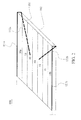
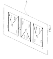
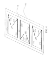
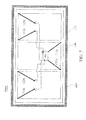
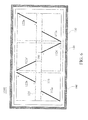
- Figures 1-5 show a method for fabricating a solar panel module according to the first embodiment of the present invention.
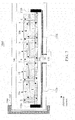
- Fig. 7 shows a schematic cross-sectional view of a solar panel module according to an embodiment of the present invention.
- Fig. 8 shows a schematic enlarged cross-sectional view detailing encapsulants and sealant used in a solar panel module according to an embodiment of the present invention.
- First prepare a plurality of solar panels 100 as shown in Fig. 1 .
- Each solar panel 100 comprises a front surface 101 and a back surface 102 and comprises a plurality of solar cell units 10a, 10b and 10 electrically connected in serial.
- Solar cell units 10a and 10b represent solar cell units at two ends of the solar panel 100 while solar cell unit 10 represents one of the solar cell units between the solar cell units 10a and 10b. Then, please refer to Fig. 2 .
- the solar panel 100 preferably has a rectangle shape with two long sides and two short sides. Dispose a front side positive ribbon 121b and a front side negative ribbon 111a at two long sides opposite to each other of the front surface 101 of the solar panel 100 and fold the front side positive ribbon 121b and the front side negative ribbon 111a back to the back surface 102 of solar panel 100 to become a backside positive ribbon 122b and a backside negative ribbon 112a respectively.
- the backside positive ribbon 122b and the backside negative ribbon 112a are shown by dashed lines to be different from the front side positive ribbon 121b and the front side negative ribbon 111a shown by solid lines.
- the front side positive ribbon 121b and the front side negative ribbon 111a are used as a positive electrode and a negative electrode of the solar panel respectively.
- the ribbons for example can be made from copper foil, copper ribbon, foils of other metals or alloy or ribbons of other metals or alloys.
- each solar panel 100 has a stacked structure from bottom to top comprising a back glass 103, a patterned lower electrode layer 2, a patterned photoelectric conversion layer 1, an optional patterned buffer layer 5 and a patterned transparent upper electrode layer 4.
- Fig. 7 focuses on the detailed structure of the solar panel 100 and the relative relations between the solar panel 100 and a back sheet 130 and a cover panel 140, so adhesives such as encapsulants and sealants are omitted in Fig. 7 . Such adhesives are shown in Fig. 8 .
- the patterned lower electrode layer 2 and the patterned transparent upper electrode layer 4 are configured to conduct electrical current generated by the patterned photoelectric conversion layer 1.
- the patterned photoelectric conversion layer 1 is configured to receive light penetrating the patterned transparent upper electrode layer 4 and the optional patterned buffer layer 5 and convert the light into electricity.
- the photoelectric conversion layer may be formed from a semiconductor material composed of copper (Cu), indium (In), gallium (Ga) and selenium (Se).
- the photoelectric conversion layer may be formed from a semiconductor compound material comprising Ib group element such as copper (Cu) or silver (Ag), IIIb group element such as aluminum (Al), gallium (Ga) or indium (In) and VIb group element such as sulfur (S), selenium (Se) or tellurium (Te).
- the transparent upper electrode layer may use indium tin oxide (ITO) and/or zinc oxide (ZnO).
- the lower electrode layer may use molybdenum (Mo).
- the back glass 103 is an unpatterned bulk dielectric structure.
- the patterned lower electrode layer 2 is formed on the back glass 103.
- the patterned photoelectric conversion layer 1 and the optional patterned buffer 5 are formed on the patterned lower electrode layer 2.
- a pattern of the lower electrode layer 2 may be used to electrically connect two solar cell units in serial such as solar cell units 10 and 10 or solar cell units 10 and 10a or solar cell units 10 and 10b.
- a pattern of the lower electrode layer 2 may also be used to electrically connect a solar cell unit 10a (or 10b) and a electrode ribbon 111a (or 121b).
- one solar cell unit 10 there is a gap (not numbered) between two adjacent patterns of the photoelectric conversion layer 1 and between two adjacent patterns of the optional buffer layer 5 and such a gap is filled with the upper transparent electrode layer 4 so the upper transparent electrode layer 4 can be electrically connected to the lower electrode 2 (physically connected in this case).
- a separation gap 6 Such a separation gap 6 would be filled with resin or other dielectric materials in a subsequent process.
- each solar cell unit 10 when light penetrates the upper transparent electrode layer 4 and the optional buffer layer 5 and reaches the photoelectric conversion layer 1, a potential of electricity would be generated in the photoelectric conversion layer 1 and results in an electrical current flowing for example from the upper transparent electrode layer 4 to the lower electrode layer 2 (shown as the dashed line arrow in Fig. 7 ).
- the electrical current would flow from the front side negative ribbon 111a through a pattern of the lower electrode layer 2, a pattern of the transparent upper electrode layer 4, a pattern of the photoelectric conversion layer 1, another pattern of the lower electrode layer 2, another pattern of the transparent upper electrode layer 4, another pattern of the photoelectric conversion layer 1 acrossto the front side positive ribbon 121b.
- the back sheet 130 is the back sheet shown in Fig. 8 and may be a rigid back sheet or a flexible back sheet.
- the size of the back sheet 130 is so chosen that its length should extend beyond the solar panels 100 (100') at two ends and its width is larger than the width of one solar panel 100(100').
- Flexible back sheet may be a high-tensile plastic sheet such as polyethylene (PE) sheet, polyamide (PA) sheet, polyethylene terephthalate (PET) sheet or a combination thereof.
- Rigid back sheet may be a tempered glass, a chemically strengthened glass or a polymeric resin sheet.
- the back sheet may also be a combination of a material from above and a metallic foil attached thereto.
- more than three solar panels 100 (100') are disposed in juxtaposed relation on a back sheet 130.
- the solar panel 100' is the same as the solar panel 100 in view of their structures but has different orientation, so the details of the solar panel 100' is omitted here.
- a method for fabricating a solar panel module of the present invention when disposing the plurality of solar panels 100 (100') one should make sure that two adjacent electrodes of two adjacent solar panels 100 and 100' are electrodes of the same electrical polarity.
- the positive electrode of a solar panel 100 is adjacent to the positive electrode of an adjacent solar panel 100' at one side while the negative electrode of the solar panel 100 is adjacent to the negative electrode of another adjacent solar panel 100' at another side opposite to said one side.
- Two adjacent electrodes of opposite polarities too close to each other may result in electrical leakage problems.
- adjacent electrodes of two adjacent solar panels 100 and 100' have the same polarity (both positive or both negative), so the shortest distance d between the adjacent electrodes of two adjacent solar panels 100 and 100' may be 2 mm or less.
- the shortest distance d between the adjacent electrodes of two adjacent solar panels 100 and 100' may be not more than 5 mm and not less than 1 mm.
- the solar panel module of the present invention can dispose more solar panel within a fixed area, thereby providing higher power per unit area.
- the back sheet 130 has a plurality of openings (not shown) and each solar panel 100 (100') corresponds to at least one opening in a central region (or other region) of said each solar panel 100 (100').
- the backside positive ribbon 122b (122b') and the backside negative ribbon 112a (112a') of each solar panel 100 (100') extend through the first encapsulant 135 and at least one of plurality of openings (not shown) and electrically connect outward (to other solar panels and to a connection box 150 which will be discussed later).
- the first encapsulant 135 for example is a thermal encapsulant such as ethylene Vinyl Acetate (EVA), polyolefin (PO) and polyvinyl butyral (PVB), or an UV curable encapsulant, or a combination thereof.
- a cover panel 140 Dispose a cover panel 140 on the plurality of solar panels 100 (100') and dispose a second encapsulant 145 between the plurality of solar panels 100 (100') and the cover panel 140 as shown in Fig. 8 .
- the cover panel 140 for example is a rigid glass panel and the size of the cover panel 140 is preferably equivalent to or smaller than the size of the back sheet 130.
- the material used for the second encapsulant 145 is similar to the material used for the first encapsulant 135 and the materials for the second encapsulant 145 and the first encapsulant 135 may be the same or different.
- the cover panel 140, the second encapsulant 145, the plurality of solar panels 100 (100'), the first encapsulant 135 and the back sheet 130 are laminated together by at least one vacuum laminating process. Since the back sheet 140 and the cover panel 130 are so sized that the lengths thereof both extend beyond solar panels 100 (100') at two ends of the plurality of solar panels and the widths thereof are both larger than a length of one solar panel 100 (100'), a first water-resistant sealant 165 can be disposed between the cover panel 130 and the back sheet 140 in a periphery region projecting from the plurality of solar panels and optionally in multiple gap regions between adjacent solar panels 100 and 100'.
- the periphery region may have a shape similar to the shape of a frame 160 shown in Figs. 5 and 6 which will be discussed later.
- the first water-resistant sealant 165 is for example thermalplastic polyolefin (TPO) or butyl rubber and is in physical contact with at least one sidewall of each solar panel 100 (100') of the plurality of the plurality of solar panels 100 (100') to protect the plurality of solar panels 100 (100') from moisture and mechanical force.
- TPO thermalplastic polyolefin
- connection box 150 Install a connection box 150 in a back surface of the back sheet as shown in Fig. 5 .
- the connection box 150 can be disposed in a central region of the back sheet 130 (corresponding to the middle solar panel) as shown in Fig. 5 or disposed in the end of the back sheet 130 (corresponding to a solar panel at the end) as shown in Fig. 7 .
- the connection box 150 can be disposed in any region of the back sheet 130. As shown in Fig.
- the backside positive ribbon 122b (122b') extending through at least one opening (not shown) of the back sheet 130 should be connected to the anode of the connection box 150 while the backside negative ribbon 112a (112a') extending through at least one opening (not shown) of the back sheet 130 should be connected to the cathode of the connection box 150.
- the solar panel module 1000 of the present invention can be fabricated according to the steps described above.
- the third encapsulant 161 is for example acrylic tape.
- the connection box 150 may further comprise a positive conductive line and a negative conductive line connecting outward (not shown) in order to electrically connect the solar panel module 1000 to an external device.
- An additional water-resistant resin layer such as a polyolefin layer may be optionally disposed on a back surface of the back sheet 130 in order to protect the connection box 150 and the back sheet 130 from moisture and mechanical force.
- FIG. 8 focuses on the distribution of the first encapsulant 135, the second encapsulant 145 and the first water-resistant sealant 165 in a case where a flexible back sheet 130 is used, so the solar panels 100 and 100' are relatively small compared to their actual sizes while the encapsulants, sealant, gaps between solar panels and distances between the back sheet and the cover panel are exaggerated.
- the flexible back sheet 130 would be closer to the cover panel 140 in an area without solar panels such as the periphery area surrounding the plurality of solar panels 100 (100') and the gap region between adjacent solar panels 100 and 100'.
- the back sheet 130 could be a rigid back sheet (not shown in Fig. 8 ) and the distance between the back sheet 130 and the cover panel 140 would be approximately the same throughout the whole solar panel module.
- Fig. 6 shows a solar panel module 1100 according to another embodiment of the present invention.
- the solar panel module 1100 is similar to the solar panel module 1000 in view of their structures.
- the differences between the solar panel modules 1100 and 1000 are the arrangement of the backside positive ribbon 122b (122b') and the backside negative ribbon 112a (112a') and the positive and negative conductive lines on the back surface of the back sheet 130.
- the backside positive ribbon 122b (122b') and the backside negative ribbon 112a (112a') of a solar panel 100 (100') are both folded from the same short side of said solar panel 100 (100') and extend therefrom.
- the backside positive ribbon 122b (122b') and the backside negative ribbon 112a (112a') of a solar panel 100 (100') are folded from different short sides of said solar panel 100 (100') and extend therefrom; the different short sides are opposite to each other.
- the positive conductive line 125 is connected to the anode of the connection box 150 and all the backside positive ribbon 122b (122b') of all the solar panels 100 (100') while the negative conductive line 115 is connected to the cathode of the connection box 150 and all the backside negative ribbon 112a (112a').
- Figs. 1-5 dispose the solar panel 100 and the solar panel 100' alternatively but the concept of disposing adjacent electrodes with the same polarity of the present invention can be applied to cases where all the solar panels have the same orientation.
- the embodiments of Figs. 1-6 have a plurality of solar panels electrically connected in parallel but the concept of disposing adjacent electrodes with the same polarity of the present invention can be applied to cases where a plurality of solar panels are electrically connected in serial.
- adjacent electrodes of two adjacent solar panels have the same polarity (both positive or both negative), so the shortest distance between the adjacent electrodes of two adjacent solar panels may be 2 mm or less.
- the solar panel module of the present invention can dispose more solar panel within a fixed area, thereby providing higher power per unit area.
- the detailed structure of solar panels shown in Fig. 7 and the distribution of encapsulants and sealant shown in Fig. 8 can be applied to the embodiment of Figs. 1-5 and the embodiment of Figs. 1-6 .
- the distribution of encapsulants and sealant shown in Fig. 8 can also be applied to a case where a solar panel module comprises only one solar panel.
Landscapes
- Engineering & Computer Science (AREA)
- Architecture (AREA)
- Civil Engineering (AREA)
- Structural Engineering (AREA)
- Photovoltaic Devices (AREA)
- Life Sciences & Earth Sciences (AREA)
- Sustainable Development (AREA)
- Sustainable Energy (AREA)
Applications Claiming Priority (1)
| Application Number | Priority Date | Filing Date | Title |
|---|---|---|---|
| TW104109142A TWI612684B (zh) | 2015-03-23 | 2015-03-23 | 太陽能板模組及其製造方法 |
Publications (2)
| Publication Number | Publication Date |
|---|---|
| EP3073636A2 true EP3073636A2 (de) | 2016-09-28 |
| EP3073636A3 EP3073636A3 (de) | 2016-10-26 |
Family
ID=53039269
Family Applications (1)
| Application Number | Title | Priority Date | Filing Date |
|---|---|---|---|
| EP15165204.7A Withdrawn EP3073636A3 (de) | 2015-03-23 | 2015-04-27 | Solarzellenmodul und verfahren zur herstellung davon |
Country Status (4)
| Country | Link |
|---|---|
| US (3) | US20160284903A1 (de) |
| EP (1) | EP3073636A3 (de) |
| CN (1) | CN106206820A (de) |
| TW (1) | TWI612684B (de) |
Cited By (1)
| Publication number | Priority date | Publication date | Assignee | Title |
|---|---|---|---|---|
| EP3496121A4 (de) * | 2016-08-02 | 2020-04-22 | Zeon Corporation | Solarzellenmodul |
Families Citing this family (3)
| Publication number | Priority date | Publication date | Assignee | Title |
|---|---|---|---|---|
| TWI769951B (zh) * | 2021-10-28 | 2022-07-01 | 曜能科技有限公司 | 太陽光電板封裝結構 |
| US20240039462A1 (en) * | 2022-07-31 | 2024-02-01 | Aptera Motors Corp. | Damper system and junction box for laminated solar panel and method of manufacture |
| TWI827509B (zh) | 2023-04-25 | 2023-12-21 | 龍佳欣實業股份有限公司 | 光電面板封裝結構及其方法 |
Citations (2)
| Publication number | Priority date | Publication date | Assignee | Title |
|---|---|---|---|---|
| US20110017279A1 (en) * | 2008-03-11 | 2011-01-27 | Joerg Baumbach | Solar module |
| EP2498297A2 (de) * | 2011-03-11 | 2012-09-12 | Auria Solar Co., Ltd. | Niederspannungs-Dünnfilm-Photovoltaikmodul |
Family Cites Families (19)
| Publication number | Priority date | Publication date | Assignee | Title |
|---|---|---|---|---|
| EP0112856A1 (de) * | 1982-07-05 | 1984-07-11 | Hartag Ag | Einrichtung mit mehreren, photoelektrische elemente enthaltenden tafeln zur erzeugung elektrischen stromes |
| WO2008150558A1 (en) * | 2007-06-08 | 2008-12-11 | Robert Stancel | Edge mountable electrical connection assembly |
| US20110239450A1 (en) * | 2008-08-11 | 2011-10-06 | Basol Bulent M | Roll-to-roll manufacturing of flexible thin film photovoltaic modules |
| AU2009292594B2 (en) * | 2008-09-10 | 2015-09-03 | Kaneka Corporation | Solar cell module, installation structure for solar cell module, and installation method for solar cell module |
| US20110214716A1 (en) * | 2009-05-12 | 2011-09-08 | Miasole | Isolated metallic flexible back sheet for solar module encapsulation |
| US20110061711A1 (en) * | 2009-09-12 | 2011-03-17 | Yuhao Luo | Building-integrated solar photovoltaic panel |
| CN102280517A (zh) * | 2010-06-11 | 2011-12-14 | 杜邦太阳能有限公司 | 太阳能电池模块及其边缘封闭的方法 |
| CN102646740B (zh) * | 2011-02-18 | 2015-06-10 | 3M创新有限公司 | 胶带及由其制成的太阳能组件和制品 |
| KR20120108723A (ko) * | 2011-03-25 | 2012-10-05 | 삼성전기주식회사 | 태양전지모듈 및 그 제조방법 |
| TWM416878U (en) * | 2011-05-06 | 2011-11-21 | Auria Solar Co Ltd | Solar cell module |
| US8497153B2 (en) * | 2011-10-31 | 2013-07-30 | E I Du Pont De Nemours And Company | Integrated back-sheet for back contact photovoltaic module |
| KR101338610B1 (ko) * | 2011-12-19 | 2013-12-06 | 엘지이노텍 주식회사 | 태양광 발전장치 및 이의 제조방법 |
| JP5780209B2 (ja) * | 2012-05-29 | 2015-09-16 | 信越化学工業株式会社 | 太陽電池モジュールの製造方法 |
| JP5958701B2 (ja) * | 2012-07-17 | 2016-08-02 | デクセリアルズ株式会社 | 配線材、太陽電池モジュール及び太陽電池モジュールの製造方法 |
| CN103280476A (zh) * | 2013-05-07 | 2013-09-04 | 友达光电股份有限公司 | 太阳能模块 |
| TWM461152U (zh) * | 2013-05-13 | 2013-09-01 | Win Win Prec Technology Co Ltd | 太陽能電池模組 |
| CN203813724U (zh) * | 2013-12-27 | 2014-09-03 | 比亚迪股份有限公司 | 双玻光伏电池组件及其边框 |
| TWM490116U (en) * | 2014-06-26 | 2014-11-11 | Gintung Energy Corp | Solar cell module |
| TWM508797U (zh) * | 2015-03-23 | 2015-09-11 | Hulk Energy Technology Co Ltd | 太陽能板模組 |
-
2015
- 2015-03-23 TW TW104109142A patent/TWI612684B/zh not_active IP Right Cessation
- 2015-04-27 EP EP15165204.7A patent/EP3073636A3/de not_active Withdrawn
- 2015-05-13 CN CN201510242432.8A patent/CN106206820A/zh active Pending
- 2015-05-14 US US14/711,826 patent/US20160284903A1/en not_active Abandoned
-
2017
- 2017-01-04 US US15/397,735 patent/US20170117427A1/en not_active Abandoned
- 2017-01-04 US US15/397,731 patent/US20170117420A1/en not_active Abandoned
Patent Citations (2)
| Publication number | Priority date | Publication date | Assignee | Title |
|---|---|---|---|---|
| US20110017279A1 (en) * | 2008-03-11 | 2011-01-27 | Joerg Baumbach | Solar module |
| EP2498297A2 (de) * | 2011-03-11 | 2012-09-12 | Auria Solar Co., Ltd. | Niederspannungs-Dünnfilm-Photovoltaikmodul |
Cited By (1)
| Publication number | Priority date | Publication date | Assignee | Title |
|---|---|---|---|---|
| EP3496121A4 (de) * | 2016-08-02 | 2020-04-22 | Zeon Corporation | Solarzellenmodul |
Also Published As
| Publication number | Publication date |
|---|---|
| TWI612684B (zh) | 2018-01-21 |
| CN106206820A (zh) | 2016-12-07 |
| US20170117420A1 (en) | 2017-04-27 |
| EP3073636A3 (de) | 2016-10-26 |
| TW201543707A (zh) | 2015-11-16 |
| US20160284903A1 (en) | 2016-09-29 |
| US20170117427A1 (en) | 2017-04-27 |
Similar Documents
| Publication | Publication Date | Title |
|---|---|---|
| US9948232B2 (en) | Method for fabricating flexible solar panel module | |
| CN106449818B (zh) | 一种带有旁路二极管的光伏叠片组件 | |
| CN101517747B (zh) | 太阳电池模块 | |
| JP7521121B2 (ja) | タンデム太陽電池 | |
| EP2043164A2 (de) | Solarzellenmodul | |
| EP3159937A1 (de) | Flexibles solarpaneelmodul | |
| US20170117420A1 (en) | Method for fabricating solar panel module | |
| WO2010010821A1 (ja) | 太陽電池モジュール及びその作成方法 | |
| CN104348408A (zh) | 接线盒及包括该接线盒的光伏模块 | |
| CN111200031B (zh) | 具有集成电子器件的薄膜光伏模块及其制造方法 | |
| CN102714231A (zh) | 太阳能电池装置和薄层太阳能模块及其制造方法 | |
| CN205336211U (zh) | 可挠式太阳能板模块 | |
| CN204680676U (zh) | 太阳能板模块 | |
| JP3204967U (ja) | 組立式のソーラーパネル設備 | |
| EP3160041B1 (de) | Solarpaneelmodul und solarpaneelvorrichtung | |
| US9252312B2 (en) | Solar cell module and manufacturing method therefor | |
| JP6134918B2 (ja) | 太陽電池モジュール | |
| US20190229674A1 (en) | Solar Panel Module and Solar Panel Apparatus | |
| JP5919494B2 (ja) | 太陽電池モジュール | |
| JP2013089751A (ja) | 太陽電池モジュール | |
| JP2013069898A (ja) | 太陽電池モジュール及びその製造方法 | |
| JP2013219233A (ja) | 太陽電池モジュール | |
| US20170207359A1 (en) | Solar cell module including wiring layer overlappingly disposed on solar cell | |
| JP2012146772A (ja) | 太陽電池モジュール及びその製造方法 |
Legal Events
| Date | Code | Title | Description |
|---|---|---|---|
| PUAI | Public reference made under article 153(3) epc to a published international application that has entered the european phase |
Free format text: ORIGINAL CODE: 0009012 |
|
| PUAL | Search report despatched |
Free format text: ORIGINAL CODE: 0009013 |
|
| 17P | Request for examination filed |
Effective date: 20150428 |
|
| AK | Designated contracting states |
Kind code of ref document: A2 Designated state(s): AL AT BE BG CH CY CZ DE DK EE ES FI FR GB GR HR HU IE IS IT LI LT LU LV MC MK MT NL NO PL PT RO RS SE SI SK SM TR |
|
| AX | Request for extension of the european patent |
Extension state: BA ME |
|
| AK | Designated contracting states |
Kind code of ref document: A3 Designated state(s): AL AT BE BG CH CY CZ DE DK EE ES FI FR GB GR HR HU IE IS IT LI LT LU LV MC MK MT NL NO PL PT RO RS SE SI SK SM TR |
|
| AX | Request for extension of the european patent |
Extension state: BA ME |
|
| RIC1 | Information provided on ipc code assigned before grant |
Ipc: H02S 40/36 20140101AFI20160922BHEP Ipc: B32B 17/10 20060101ALI20160922BHEP Ipc: H01L 31/05 20060101ALI20160922BHEP Ipc: H02S 30/20 20140101ALI20160922BHEP Ipc: H01L 31/02 20060101ALI20160922BHEP Ipc: H02S 20/23 20140101ALI20160922BHEP Ipc: H01L 31/048 20060101ALI20160922BHEP |
|
| RAP1 | Party data changed (applicant data changed or rights of an application transferred) |
Owner name: ETERBRIGHT SOLAR CORPORATION |
|
| 17Q | First examination report despatched |
Effective date: 20170822 |
|
| STAA | Information on the status of an ep patent application or granted ep patent |
Free format text: STATUS: THE APPLICATION IS DEEMED TO BE WITHDRAWN |
|
| 18D | Application deemed to be withdrawn |
Effective date: 20180103 |