EP3076211B1 - Kupplungsverfahren und kupplungsvorrichtung für lichtwellenleiter und einfachmodus-glasfaser - Google Patents
Kupplungsverfahren und kupplungsvorrichtung für lichtwellenleiter und einfachmodus-glasfaser Download PDFInfo
- Publication number
- EP3076211B1 EP3076211B1 EP13899434.8A EP13899434A EP3076211B1 EP 3076211 B1 EP3076211 B1 EP 3076211B1 EP 13899434 A EP13899434 A EP 13899434A EP 3076211 B1 EP3076211 B1 EP 3076211B1
- Authority
- EP
- European Patent Office
- Prior art keywords
- optical waveguide
- mode fiber
- fiber
- taper structure
- optical
- Prior art date
- Legal status (The legal status is an assumption and is not a legal conclusion. Google has not performed a legal analysis and makes no representation as to the accuracy of the status listed.)
- Active
Links
Images


Classifications
-
- G—PHYSICS
- G02—OPTICS
- G02B—OPTICAL ELEMENTS, SYSTEMS OR APPARATUS
- G02B6/00—Light guides; Structural details of arrangements comprising light guides and other optical elements, e.g. couplings
- G02B6/24—Coupling light guides
- G02B6/26—Optical coupling means
- G02B6/30—Optical coupling means for use between fibre and thin-film device
- G02B6/305—Optical coupling means for use between fibre and thin-film device and having an integrated mode-size expanding section, e.g. tapered waveguide
-
- G—PHYSICS
- G02—OPTICS
- G02B—OPTICAL ELEMENTS, SYSTEMS OR APPARATUS
- G02B6/00—Light guides; Structural details of arrangements comprising light guides and other optical elements, e.g. couplings
- G02B6/10—Light guides; Structural details of arrangements comprising light guides and other optical elements, e.g. couplings of the optical waveguide type
- G02B6/12—Light guides; Structural details of arrangements comprising light guides and other optical elements, e.g. couplings of the optical waveguide type of the integrated circuit kind
- G02B6/122—Basic optical elements, e.g. light-guiding paths
- G02B6/1221—Basic optical elements, e.g. light-guiding paths made from organic materials
-
- G—PHYSICS
- G02—OPTICS
- G02B—OPTICAL ELEMENTS, SYSTEMS OR APPARATUS
- G02B6/00—Light guides; Structural details of arrangements comprising light guides and other optical elements, e.g. couplings
- G02B6/10—Light guides; Structural details of arrangements comprising light guides and other optical elements, e.g. couplings of the optical waveguide type
- G02B6/12—Light guides; Structural details of arrangements comprising light guides and other optical elements, e.g. couplings of the optical waveguide type of the integrated circuit kind
- G02B6/13—Integrated optical circuits characterised by the manufacturing method
- G02B6/132—Integrated optical circuits characterised by the manufacturing method by deposition of thin films
-
- G—PHYSICS
- G02—OPTICS
- G02B—OPTICAL ELEMENTS, SYSTEMS OR APPARATUS
- G02B6/00—Light guides; Structural details of arrangements comprising light guides and other optical elements, e.g. couplings
- G02B6/10—Light guides; Structural details of arrangements comprising light guides and other optical elements, e.g. couplings of the optical waveguide type
- G02B6/12—Light guides; Structural details of arrangements comprising light guides and other optical elements, e.g. couplings of the optical waveguide type of the integrated circuit kind
- G02B6/13—Integrated optical circuits characterised by the manufacturing method
- G02B6/138—Integrated optical circuits characterised by the manufacturing method by using polymerisation
Definitions
- Embodiments of the present invention relate to the communications field, and specifically, to a method and an apparatus for coupling an optical waveguide to a single-mode fiber.
- a silicon waveguide Silicon Waveguide
- SOI silicon on insulator
- an SOI manufacturing process has advantages of being compatible with a traditional complementary metal-oxide-semiconductor (Complementary Metal-Oxide-Semiconductor, CMOS) process and being able to implement integration between a photonic device and an electronic device. Therefore, the SOI material has become a main material for preparing an integrated optical waveguide device and has a wide application prospect.
- CMOS complementary Metal-oxide-semiconductor
- a critical issue is that when an optical signal is input and output to implement communication between the device and an off-chip optical system, especially when current luminous efficiency of silicon does not meet a practical requirement, an optical fiber needs to be used to introduce a light source from the outside of an optical waveguide.
- the integrated optical waveguide has a strong binding capability for a light field
- a spot size of the integrated optical waveguide is approximately on an order of hundreds of nanometers and a mode field shape of the integrated optical waveguide is generally an ellipse
- a common single-mode fiber has a weaker binding capability for the light field
- a spot size of the common single-mode fiber is generally about 10 ⁇ m and a mode field shape of the common single-mode fiber is a circle.
- An inverted taper-based spot-size converter method (Inverted Taper-Based Spot-Size Converter Method) is a commonly-used transverse coupling method.
- a principle of the coupling method is: using an inverted taper structure 121 whose width is gradually decreased and that is disposed at an end of a silicon waveguide 120 to enlarge a small-size spot of the silicon waveguide 120, and disposing, at the inverted taper structure 121 of the silicon waveguide 120, a low refractive index optical waveguide 130 wrapping the inverted taper structure 121, so that a mode field in the silicon waveguide 120 gradually separates from the silicon waveguide 120 and is transferred into the low refractive index optical waveguide 130, thereby enlarging a size of a mode field that transmits light to enable the size to be close to a size of a mode field of a single-mode fiber; and then forming a locating slot (for example, V-shaped slot) 150 at one side, opposite to the silicon waveguide 120,
- the inverted taper-based spot-size converter method has relatively high coupling efficiency and a broadband coupling feature, and the coupling efficiency is insensitive to polarization that is for transmitting light.
- the coupling method has the following disadvantages: First, because a mode field diameter of the silicon waveguide that is enlarged by using the inverted taper structure is still relatively small (about 3 ⁇ m), the single-mode fiber still needs to be perfectly aligned with the low refractive index optical waveguide. For example, if the single-mode fiber uses a lensed fiber whose terminal diameter is 3 ⁇ m, 1 dB alignment tolerance between the single-mode fiber and the low refractive index optical waveguide is about ⁇ 0.3 ⁇ m.
- the coupling method has a very high precision requirement on a packaging device.
- the coupling method usually requires active coupling to ensure coupling efficiency, which increases coupling complexity.
- polishing processing generally needs to be performed on an end face of the low refractive index optical waveguide, and an anti-reflection film (Anti-Reflection Film) needs to be coated on the end face of the low refractive index optical waveguide, or refractive index matching liquids (Refractive Index Matching Liquids) are added between the end face of the low refractive index optical waveguide and a terminal of the single-mode fiber to reduce Fresnel reflection on the end face.
- Anti-Reflection Film Anti-Reflection Film
- refractive index matching liquids Refractive Index Matching Liquids
- the coupling method requires very high alignment precision, the method is relatively difficult to implement coupling between an optical waveguide and a fiber array and is not applicable to coupling and packaging for an optical chip having high-density input and output interfaces.
- it is a problem that urgently needs to be resolved in the art as how to reduce a requirement on alignment precision on the basis of ensuring coupling efficiency between an optical waveguide and a single-mode fiber, so as to lower a requirement of coupling on a device, reduce packaging costs, and implement coupling between an optical waveguide array and a single-mode fiber array.
- CN 101533128 A relates to a silicon nanometer optical waveguide and optical fiber coupling and encapsulation method in the technical field of optical integrated chip coupling and encapsulation.
- US 2009/0087144 A1 relates to an optical coupling device for coupling an optical signal propagating in an optical fiber or space to an optical waveguide.
- JP 2013-64852 A relates to a spot size converter comprises: a BOX layer 5 to be an under cladding; a first silicon core 6; a tapered part 7; a second silicon core 8; and an over cladding 9.
- US 7,664,352 B1 relates to a spot size converter has a first core, a larger second core, and a clad disposed on a substrate.
- WO 03/044580 A2 relates to a high efficiency optical mode transformer for matching an optical single or multimode fiber with a high-index contrast planar waveguide on a semiconductor or dielectric microchip.
- JP S56-55086 A relates to a semiconductor laser device with coupling circuit.
- JPH09159865 relates to a waveguide evanecsently coupled to a tapered fibre end.
- US 2012/0224820 A1 relates to a spot-size converter.
- JP 05209331 relates to a waveguide type beam spot conversion element and production thereof.
- the present invention provides a method for coupling an optical waveguide to a single-mode fibre according to claim 1 and an apparatus for coupling an optical waveguide to a single-mode fibre according to claim 7 which can lower an alignment precision requirement on a coupling device and reduce production costs.
- a method for coupling an optical waveguide to a single-mode fiber including: forming a locating slot on a substrate, where a first optical waveguide is further disposed on the substrate, one end of the first optical waveguide has an inverted taper structure whose width is gradually decreased along a direction of the locating slot, and a center line, passing through a taper tip, of the inverted taper structure is parallel to a center line of the locating slot; fastening, into the locating slot, a single-mode fiber with one end having an optical fiber taper structure whose diameter is gradually decreased along a direction of the locating slot, where the end, having the optical fiber taper structure, of the single-mode fiber is disposed opposite to the end, having the inverted taper structure, of the first optical waveguide; and disposing a second optical waveguide on the substrate according to a location of the first optical waveguide and a location of the single-mode fiber, so that the second optical waveguide is located between the first optical waveguide and the
- the disposing a second optical waveguide on the substrate according to a location of the first optical waveguide and a location of the single-mode fiber includes: determining a location of a terminal of the end, having the optical fiber taper structure, of the single-mode fiber and a location of a terminal of the end, having the inverted taper structure, of the first optical waveguide; determining a path of the second optical waveguide on the substrate according to the location of the terminal of the end, having the optical fiber taper structure, of the single-mode fiber and the location of the terminal of the end, having the inverted taper structure, of the first optical waveguide; and disposing the second optical waveguide on the substrate according to the path of the second optical waveguide on the substrate.
- the determining a path of the second optical waveguide on the substrate according to the location of the terminal of the end, having the optical fiber taper structure, of the single-mode fiber and the location of the terminal of the end, having the inverted taper structure, of the first optical waveguide includes: determining a path with a smallest loss among all possible paths according to the location of the terminal of the end, having the optical fiber taper structure, of the single-mode fiber and the location of the terminal of the end, having the inverted taper structure, of the first optical waveguide, wherein the path with the smallest loss is a path of a smallest length; and using the path with a smallest loss as the path of the second optical waveguide on the substrate.
- the disposing the second optical waveguide on the substrate according to the path of the second optical waveguide on the substrate includes: spin-coating a layer of ultraviolet-sensitive polymer material on the substrate; and performing direct writing on the ultraviolet-sensitive polymer material along the path of the second optical waveguide on the substrate by using an ultraviolet laser, so as to form the second optical waveguide.
- the forming a locating slot on a substrate includes: setting a section size of the locating slot, so that when the single-mode fiber is horizontally fastened into the locating slot, the terminal of the end, having the optical fiber taper structure, of the single-mode fiber is above an upper surface of the substrate.
- a diameter of a taper tip of the optical fiber taper structure is less than 3 ⁇ m.
- an apparatus for coupling an optical waveguide to a single-mode fiber including at least one optical waveguide-fiber coupling unit, where a first optical waveguide-fiber coupling unit of the at least one optical waveguide-fiber coupling unit includes: a substrate, where a locating slot is formed on the substrate; a first optical waveguide disposed on the substrate, where one end of the first optical waveguide has an inverted taper structure whose width is gradually decreased along a direction of the locating slot, and a center line, passing through a taper tip, of the inverted taper structure is parallel to a center line of the locating slot; a single-mode fiber disposed in the locating slot, where one end of the single-mode fiber has an optical fiber taper structure whose diameter is gradually decreased along a direction of the first optical waveguide, and the end, having the optical fiber taper structure, of the single-mode fiber is disposed opposite to the end, having the inverted taper structure, of the first optical waveguide; and a second optical waveguide
- a path of the second optical waveguide on the substrate is a path with a smallest loss among all possible paths determined according to a location of a terminal of the end, having the inverted taper structure, of the first optical waveguide and a location of a terminal of the end, having the optical fiber taper structure, of the single-mode fiber, and wherein the path with a smallest loss is a path of a smallest length of all paths.
- a diameter of a taper tip of the optical fiber taper structure is less than 3 ⁇ m.
- one end of a first optical waveguide is set to have an inverted taper structure, to enlarge a spot size of the first optical waveguide
- one end of a single-mode fiber is set to have an optical fiber taper structure, to diminish a spot size of the single-mode fiber
- a second optical waveguide is disposed according to locations of the first optical waveguide and the single-mode fiber, so as to implement alignment and coupling between the first optical waveguide and the single-mode fiber by using the second optical waveguide.
- the first optical waveguide and the single-mode fiber do not need to be precisely aligned, as long as center lines of the first optical waveguide and the single-mode fiber are parallel, thereby improving an alignment tolerance between the first optical waveguide and the single-mode fiber, lowering an alignment precision requirement on a coupling device and reducing production costs, and increasing a possibility of industrializing an integrated optical waveguide chip.
- FIG. 2 is a schematic flowchart of a method 200 for coupling an optical waveguide to a single-mode fibre.
- the method may be executed by an apparatus for coupling an optical waveguide to a single-mode fiber.
- the method 200 includes: S210: Form a locating slot on a substrate, where a first optical waveguide is further disposed on the substrate, one end of the first optical waveguide has an inverted taper structure whose width is gradually decreased, and a center line, passing through a taper tip, of the inverted taper structure is parallel to a center line of the locating slot.
- the first optical waveguide is any integrated optical waveguide.
- the first optical waveguide may be a silicon waveguide, that is, a silicon-based optical waveguide, and correspondingly, the substrate may be an SOI substrate; the first optical waveguide may also be a polymer optical waveguide, for example, an optical waveguide in an opto-electric hybrid printed circuit board (Opto-Electric Hybrid Printed Circuit Board, OE-PCB).
- OE-PCB opto-electric hybrid printed circuit board
- the first optical waveguide is disposed at one side on an upper surface of the substrate, and one end of the first optical waveguide is processed to have the inverted taper structure, where the width of the inverted taper structure is gradually decreased along a direction of the locating slot, so that a size of a mode field that is transmitted in the first optical waveguide is gradually enlarged and a light field that is limited to being transmitted in the first optical waveguide gradually separates from the first optical waveguide and is transferred to the outside of the first optical waveguide.
- the inverted taper structure may be processed by using a photolithography process, an electron-beam lithography process, or the like, which is not limited in this example.
- a width of the taper tip of the inverted taper structure is less than 100 nm, and a length of a taper area of the inverted taper structure has an order of hundreds of micrometers.
- a slope of the inverted taper structure may be set according to an actual requirement. Generally, a smaller slope indicates a larger length of the inverted taper structure.
- the inverted taper structure can meet an adiabatic transition condition, so that the first optical waveguide has a smallest structural loss, but this example is not limited thereto.
- the locating slot may be generated by using any anisotropic etching method.
- a locating slot 23 may be formed on one side, opposite to a first optical waveguide 22, on the upper surface of a substrate 21, and the center line of the locating slot 23 is parallel to the center line, passing through the taper tip, of an inverted taper structure 22a of the first optical waveguide 22, where a transverse distance between the taper tip of the inverted taper structure 22a and the center line of the locating slot 23 may be less than a preset threshold (100 ⁇ m), and the preset threshold may depend on processing precision of the locating slot 23 and layouts of coupling units of the apparatus for coupling an optical waveguide to a single-mode fiber.
- a preset threshold 100 ⁇ m
- the taper tip of the inverted taper structure 22a may be basically aligned with the center line of the locating slot 23, that is, the center line, passing through the taper tip, of the inverted taper structure 22a basically coincides with the center line of the locating slot 23.
- the first optical waveguide 22 is basically aligned with a single-mode fiber that is subsequently fastened into the locating slot 23, but this example is not limited thereto.
- S220 Fasten, into the locating slot, a single-mode fiber with one end having an optical fiber taper structure whose diameter is gradually decreased, where the end, having the optical fiber taper structure, of the single-mode fiber is disposed opposite to the end, having the inverted taper structure, of the first optical waveguide.
- One end of the single-mode fiber is processed to have the optical fiber taper structure, where the diameter of the optical fiber taper structure is gradually decreased along a direction of the first optical waveguide, so that a spot size of the single-mode fiber is decreased.
- the spot size of the single-mode fiber may be decreased from 10 ⁇ m to an order of a submicrometer by using the optical fiber taper structure.
- a diameter of a taper tip of the optical fiber taper structure of the single-mode fiber may be less than 3 ⁇ m, and the optical fiber taper structure may be prepared by using a heating method, a chemical etching method, or the like, where the heating method may be flame heating, laser heating, electric heating, or the like, and this example is not limited thereto.
- the single-mode fiber may be horizontally fastened and packaged in the locating slot by using an ultraviolet curing adhesive, and the end, having the optical fiber taper structure, of the single-mode fiber may extend out of the locating slot along the direction of the first optical waveguide.
- the end, having the optical fiber taper structure 24a, of the single-mode fiber 24 may extend out of the locating slot 23 by an appropriate length, and the extended length may be dozens of micrometers.
- a line in which a terminal of the end, having the optical fiber taper structure 24a, of the single-mode fiber 24 is located may be parallel to a line in which a terminal of the end, having the inverted taper structure 22a, of the first optical waveguide 22 is located.
- the terminal of the single-mode fiber 24 may be basically aligned with the terminal of the first optical waveguide 22, but this example is not limited thereto.
- S230 Dispose a second optical waveguide on the substrate according to a location of the first optical waveguide and a location of the single-mode fiber, so that the second optical waveguide is located between the first optical waveguide and the single-mode fiber, the second optical waveguide is optically coupled to the first optical waveguide by using the end, having the inverted taper structure, of the first optical waveguide, and the second optical waveguide is optically coupled to the single-mode fiber by using the end, having the optical fiber taper structure, of the single-mode fiber.
- the second optical waveguide 25 is located between the first optical waveguide 22 and the single-mode fiber 24, and the second optical waveguide 25 is optically coupled to the first optical waveguide 22 and the single-mode fiber 24, so as to implement optical coupling between the first optical waveguide 22 and the single-mode fiber 24.
- a path of the second optical waveguide 25 on the substrate 21 may be set according to the location of the first optical waveguide 22, a location of the single-mode fiber 24, and a manner of optical coupling between the second optical waveguide 25 and the first optical waveguide 22 and a manner of optical coupling between the second optical waveguide 25 and the single-mode fiber 24.
- the second optical waveguide 25 may be optically coupled to the first optical waveguide 22 and the single-mode fiber 24 in various manners.
- one end of a first optical waveguide is set to have an inverted taper structure, to enlarge a spot size of the first optical waveguide
- one end of a single-mode fiber is set to have an optical fiber taper structure, to diminish a spot size of the single-mode fiber
- a second optical waveguide is disposed according to locations of the first optical waveguide and the single-mode fiber, so as to implement alignment and coupling between the first optical waveguide and the single-mode fiber by using the second optical waveguide.
- the first optical waveguide and the single-mode fiber do not need to be precisely aligned, as long as center lines of the first optical waveguide and the single-mode fiber are parallel, thereby improving an alignment tolerance between the first optical waveguide and the single-mode fiber, lowering an alignment precision requirement on a coupling device and reducing production costs, and increasing a possibility of industrializing an integrated optical waveguide chip.
- the locating slot may have multiple different shapes.
- the locating slot may be a U-shaped slot, a V-shaped slot, or a rectangular slot.
- the locating slot shown in FIG. 3 to FIG 5 is a V-shaped slot.
- S210 of forming a locating slot on a substrate includes: S211: Set a section size of the locating slot, so that when the single-mode fiber is horizontally fastened into the locating slot, the terminal of the end, having the optical fiber taper structure, of the single-mode fiber is above an upper surface of the substrate.
- the section size of the locating slot 23 is set so that the terminal of the end, having the optical fiber taper structure 24a, of the single-mode fiber 24 is above the upper surface of the substrate 21, where a distance between the terminal and the upper surface may be 1 ⁇ m to 5 ⁇ m.
- a height between the terminal of the end, having the optical fiber taper structure 24a, of the single-mode fiber 24 and the upper surface of the substrate 21 may be a half of a height of the second optical waveguide 25.
- the second optical waveguide is optically coupled to the first optical waveguide by using the end, having the inverted taper structure, of the first optical waveguide
- the second optical waveguide is optically coupled to the single-mode fiber by using the end, having the optical fiber taper structure, of the single-mode fiber
- S230a Dispose the second optical waveguide on the substrate, so that the end, having the inverted taper structure, of the first optical waveguide and the end, having the optical fiber taper structure, of the single-mode fiber are both embedded in the second optical waveguide.
- both the end, having the inverted taper structure, of the first optical waveguide and the end, having the optical fiber taper structure, of the single-mode fiber may be wrapped in the second optical waveguide; in this way, a partial structure of the first optical waveguide and a partial structure of the single-mode fiber are both located in the second optical waveguide, thereby implementing that the second optical waveguide is optically coupled to the first optical waveguide and the single-mode fiber.
- both the end, having the inverted taper structure 22a, of the first optical waveguide 22 and the end, having the optical fiber taper structure 24a, of the single-mode fiber 24 may be embedded near a central axis of the second optical waveguide 25, so as to implement optical coupling between the second optical waveguide 25 the first optical waveguide 22 and between the second optical waveguide 25 and the single-mode fiber 24.
- S230 of disposing a second optical waveguide on the substrate, so that the second optical waveguide is located between the first optical waveguide and the single-mode fiber, the second optical waveguide is optically coupled to the first optical waveguide by using the end, having the inverted taper structure, of the first optical waveguide, and the second optical waveguide is optically coupled to the single-mode fiber by using the end, having the optical fiber taper structure, of the single-mode fiber includes: S230b: Dispose the second optical waveguide on the substrate, so that the end, having the inverted taper structure, of the first optical waveguide is embedded in the second optical waveguide, and the end, having the optical fiber taper structure, of the single-mode fiber is optically coupled to the second optical waveguide by using an evanescent field.
- the evanescent field herein refers to an electromagnetic wave field that is generated through total reflection and transmitted on a surface of a waveguide and whose strength exponentially decays as a vertical depth increases.
- the end, having the optical fiber taper structure 24a, of the single-mode fiber 24 may be close to the second optical waveguide 25 within a particular distance, for example, within about 100 nm.
- a side face of the terminal of the end, having the optical fiber taper structure 24a, of the single-mode fiber 24 may also be partially overlapped with the second optical waveguide 25, that is, a part of the end, having the optical fiber taper structure 24a, of the single-mode fiber 24 is embedded in the second optical waveguide 25, but this embodiment of the present invention is not limited thereto.
- the path of the second optical waveguide on the substrate may be set by depending on the location of the first optical waveguide, the location of the single-mode fiber, and a manner of coupling between the second optical waveguide and the first optical waveguide and between the second optical waveguide and the single-mode fiber.
- disposing the second optical waveguide on the substrate in S230 or S230a or S230b includes:
- the location of the terminal of the end, having the optical fiber taper structure, of the single-mode fiber and the location of the terminal of the end, having the inverted taper structure, of the first optical waveguide may be determined by means of machine visual aids, so that accurate locations of the terminals of the first optical waveguide and the single-mode fiber are determined more precisely, and the path of the second optical waveguide on the substrate may be determined according to a location of the taper tip of the inverted taper structure, a location of the taper tip of the optical fiber taper structure, and the manner of coupling between the second optical waveguide and the first optical waveguide and between the second optical waveguide and the single-mode fiber.
- a part of the inverted taper structure may be embedded in the second optical waveguide and a part of the optical fiber taper structure be embedded in the second optical waveguide, or according to the path of the second optical waveguide, a part of the inverted taper structure may be embedded at one side of the second optical waveguide, and the other side of the second optical waveguide may be close to the optical fiber taper structure within a particular distance, but this embodiment of the present invention is not limited thereto.
- the transverse distance between the taper tip of the inverted taper structure and the center line of the locating slot may not be zero, and the path of the second optical waveguide on the substrate may be bended; in this case, the path of the second optical waveguide is also set by depending on a transmission loss of the second optical waveguide, and specifically, the path of the second optical waveguide on the substrate may also be a path with a relatively small transmission loss among all possible paths.
- the path of the second optical waveguide may be set to be slightly bended, so that the second optical waveguide has a relatively small transmission loss, but this example is not limited thereto.
- S232 of determining a path of the second optical waveguide on the substrate according to the location of the terminal of the end, having the optical fiber taper structure, of the single-mode fiber and the location of the terminal of the end, having the inverted taper structure, of the first optical waveguide includes:
- the "loss" herein may refer to total losses of each path, where a total loss of a path may include a transmission loss and a bending loss; the transmission loss depends on a length of the path, and generally, a longer path indicates a larger transmission loss; the bending loss depends on a bending radius of a bending part of the path, and generally, a smaller bending radius indicates a larger bending loss. Therefore, generally, the path with a smallest loss may be a path of a small length and on which no obvious bending exists. Optionally, if all paths have no obvious bending, a path of a smallest length may serve as the path with a smallest loss, but this example is not limited thereto.
- the second optical waveguide may be disposed on the foregoing determined path of the second optical waveguide in multiple manners.
- S233 of disposing the second optical waveguide on the substrate according to the path of the second optical waveguide on the substrate includes:
- spin-coat herein refers to a process in which a polymer solution is homogeneously coated on SOI by means of high-speed rotation of an SOI chip
- direct writing refers to implementing the second optical waveguide by using a laser direct writing process, that is, manufacturing the second optical waveguide by controlling direct exposure of a motion path, of a laser beam focus, on a light sensitive polymer material by using an ultraviolet laser.
- the second optical waveguide is a polymer optical waveguide.
- a thickness of the ultraviolet-sensitive polymer material may be about 3 ⁇ m.
- the second optical waveguide may also be prepared by using another method.
- quantities of locating slots, first optical waveguides, second optical waveguides, and single-mode fibers are the same and may be one or more.
- the method for coupling an optical waveguide to a single-mode fiber in this embodiment of the present invention can implement coupling between a single-mode fiber array and an integrated optical waveguide array. Specifically, as shown in FIG.
- the method for coupling an optical waveguide to a single-mode fiber includes the following steps:
- the i th single-mode fiber 24 (i) of the N single-mode fibers is fastened into the i th locating slot 23 (i) , and one end, having an optical fiber taper structure 24a (i) , of the i th single-mode fiber 24 (i) is disposed near the i th first optical waveguide 22 (i) , and a terminal of the end, having the optical fiber taper structure 24a (i) , of the i th single-mode fiber 24 (i) is above the upper surface of the substrate 21.
- Both a terminal of the i th first optical waveguide 22 (i) and the terminal of the i th single-mode fiber 24 (i) may be embedded in the i th second optical waveguide 25 (i) , or, according to the invention, a terminal of the i th first optical waveguide 22 (i) is embedded in the i th second optical waveguide 25 (i) and the terminal of the i th single-mode fiber 24 (i) is optically coupled to the i th second optical waveguide 25 (i) by using an evanescent field.
- one end of a first optical waveguide is set to have an inverted taper structure, to enlarge a spot size of the first optical waveguide
- one end of a single-mode fiber is set to have an optical fiber taper structure, to diminish a spot size of the single-mode fiber
- a second optical waveguide is disposed according to locations of the first optical waveguide and the single-mode fiber, so as to implement alignment and coupling between the first optical waveguide and the single-mode fiber by using the second optical waveguide.
- the first optical waveguide and the single-mode fiber do not need to be precisely aligned, as long as center lines of the first optical waveguide and the single-mode fiber are parallel, thereby improving an alignment tolerance between the first optical waveguide and the single-mode fiber, lowering an alignment precision requirement on a coupling device and reducing production costs, and increasing a possibility of industrializing an integrated optical waveguide chip.
- sequence numbers of the foregoing processes do not mean execution sequences, and the execution sequences of the processes shall be determined according to functions and internal logic of the processes, and shall not be construed as any limitation to the implementation processes of the embodiments of the present invention.
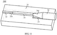
- FIG. 11 is a schematic block diagram of an apparatus 300 for coupling an optical waveguide to a single-mode fiber
- the apparatus 300 includes at least one optical waveguide-fiber coupling unit, and a first optical waveguide-fiber coupling unit of the at least one optical waveguide-fiber coupling unit includes:
- the locating slot 33 and the first optical waveguide 32 are respectively located at two opposite sides on an upper surface of the substrate 31, and the center line, passing through the taper tip, of the inverted taper structure 32a is parallel to the center line of the locating slot 33.
- a distance between the center line, passing through the taper tip, of the inverted taper structure 32a and the center line of the locating slot 33 may be less than a preset threshold (100 ⁇ m), and the preset threshold may depend on processing precision of the locating slot 33 and layouts of the optical waveguide-fiber coupling unit.
- the taper tip of the inverted taper structure 32a may be basically aligned with the center line of the locating slot 33, that is, the center line, passing through the taper tip, of the inverted taper structure 32a may basically coincide with the center line of the locating slot 33, so that the first optical waveguide 32 is basically aligned with the single-mode fiber 34 that is fastened into the locating slot 33, thereby reducing complexity of a path of the second optical waveguide 35 on the substrate.
- other optical waveguide-fiber coupling units in the apparatus for coupling an optical waveguide to a single-mode fiber than the first optical waveguide-fiber coupling unit may have structures that are the same as a structure of the first optical waveguide-fiber coupling unit; in this case, the apparatus for coupling an optical waveguide to a single-mode fiber implements coupling between an optical waveguide array and a single-mode fiber array.
- the other optical waveguide-fiber coupling units in the apparatus for coupling an optical waveguide to a single-mode fiber may also have structures that are different from the structure of the first optical waveguide-fiber coupling unit.
- one end of a first optical waveguide is set to have an inverted taper structure, to enlarge a spot size of the first optical waveguide
- one end of a single-mode fiber is set to have an optical fiber taper structure, to diminish a spot size of the single-mode fiber
- a second optical waveguide is disposed according to locations of the first optical waveguide and the single-mode fiber, so as to implement alignment and coupling between the first optical waveguide and the single-mode fiber by using the second optical waveguide.
- the first optical waveguide and the single-mode fiber do not need to be precisely aligned, as long as center lines of the first optical waveguide and the single-mode fiber are parallel, thereby improving an alignment tolerance between the first optical waveguide and the single-mode fiber, lowering an alignment precision requirement on a coupling device and reducing production costs, and increasing a possibility of industrializing an integrated optical waveguide chip.
- the first optical waveguide may be any integrated optical waveguide.
- the first optical waveguide is a silicon waveguide, that is, a silicon-based optical waveguide, and correspondingly, the substrate may be an SOI substrate; the first optical waveguide may also be a polymer optical waveguide, for example, an optical waveguide in an opto-electric hybrid printed circuit board (Opto-Electric Hybrid Printed Circuit Board, OE-PCB).
- OE-PCB opto-electric hybrid printed circuit board
- One end of the first optical waveguide is set to have the inverted taper structure, where the width of the inverted taper structure is gradually decreased along a direction of the single-mode fiber, so that a size of a mode field that is transmitted in the first optical waveguide is gradually enlarged and a light field that is limited to being transmitted in the first optical waveguide gradually separates from a limitation of the first optical waveguide and is transferred to the outside of the first optical waveguide.
- a width of the taper tip of the inverted taper structure is less than 100 nm, and a length of a taper area of the inverted taper structure has an order of hundreds of micrometers.
- a slope of the inverted taper structure may be set according to an actual requirement. Generally, a smaller slope indicates a larger length of the inverted taper structure.
- the inverted taper structure can meet an adiabatic transition condition, so that the first optical waveguide has a smallest structural loss, but this embodiment of the present invention is not limited thereto.
- One end of the single-mode fiber has the optical fiber taper structure, where the diameter of the optical fiber taper structure is gradually decreased along a direction of the first optical waveguide, so that a spot size of the single-mode fiber is decreased.
- the spot size of the single-mode fiber may be decreased from 10 ⁇ m to an order of a submicrometer by using the optical fiber taper structure.
- a diameter of a taper tip of the optical fiber taper structure of the single-mode fiber is less than 3 microns.
- the apparatus for coupling an optical waveguide to a single-mode fiber in the present invention implements coupling and alignment between the first optical waveguide and the single-mode fiber mainly by using the second optical waveguide; therefore, the locating slot may have multiple different shapes.
- the locating slot may be a U-shaped slot, a V-shaped slot, or a rectangular slot.
- a section size of the locating slot is set so that a terminal of the end, having the optical fiber taper structure, of the single-mode fiber is above an upper surface of the substrate, where a distance between the terminal and the upper surface may be 1 ⁇ m to 5 ⁇ m.
- a height between the terminal of the end, having the optical fiber taper structure, of the single-mode fiber and the upper surface of the substrate may be a half of a height of the second optical waveguide.
- the single-mode fiber is horizontally fastened into the locating slot, and the end, having the optical fiber taper structure, of the single-mode fiber may extend out of the locating slot along the direction of the first optical waveguide.
- the single-mode fiber may be fastened and packaged in the locating slot by using an ultraviolet curing adhesive, a length by which the end, having the optical fiber taper structure, of the single-mode fiber extends out of the locating slot may be dozens of micrometers, and the terminal of the end, having the optical fiber taper structure, of the single-mode fiber may be basically aligned with a terminal of the end, having the inverted taper structure, of the first optical waveguide.
- the end, having the inverted taper structure, of the first optical waveguide is embedded in the second optical waveguide, and the end, having the optical fiber taper structure, of the single-mode fiber is optically coupled to the second optical waveguide by using an evanescent field.
- the end, having the optical fiber taper structure, of the single-mode fiber may be close to the second optical waveguide within a particular distance, for example, within about 100 nm, and a side face of the terminal of the end, having the optical fiber taper structure, of the single-mode fiber may also be partially overlapped with the second optical waveguide, that is, a part of the end, having the optical fiber taper structure, of the single-mode fiber is embedded in the second optical waveguide
- the path of the second optical waveguide on the substrate is set by depending on the location of the first optical waveguide, the location of the single-mode fiber, and a manner of coupling between the second optical waveguide and the first optical waveguide and coupling between the second optical waveguide and the single-mode fiber.
- accurate locations of the terminals of the first optical waveguide and the single-mode fiber may also be determined by using a machine visual aid system, and the path of the second optical waveguide is calculated according to the location of the first optical waveguide, the location of the single-mode fiber, and a mathematical calculation method.
- the second optical waveguide needs to be optically coupled to the first optical waveguide and the single-mode fiber, and the second optical waveguide also needs to have a relatively small loss, that is, have a relatively small transmission loss and bending loss.
- the path of the second optical waveguide may have a relatively small path length and have no obvious bending, so as to reduce the transmission loss and the bending loss.
- the path of the second optical waveguide on the substrate is a path with a smallest loss among all possible paths determined according to the location of the terminal of the end, having the inverted taper structure, of the first optical waveguide and the location of the terminal of the end, having the optical fiber taper structure, of the single-mode fiber, that is, a path of which the sum of a transmission loss and a bending loss is the smallest among all the possible paths
- the second optical waveguide may be prepared along the determined path in multiple manners.
- the second optical waveguide may be prepared by using an ultraviolet laser direct writing method.
- the second optical waveguide is obtained by performing direct writing, along the path with a smallest loss by using an ultraviolet laser, on an ultraviolet-sensitive polymer material spin-coated on the substrate.
- a layer of ultraviolet-sensitive polymer material may be spin-coated on the substrate first, where a thickness of the ultraviolet-sensitive polymer material may be about 3 ⁇ m, and then direct writing is performed on the ultraviolet-sensitive polymer material along the determined path of the second optical waveguide by using the ultraviolet laser to obtain the second optical waveguide.
- the apparatus 300 for coupling an optical waveguide to a single-mode fiber may be coupled and packaged by using the method for coupling an optical waveguide to a single-mode fiber shown in FIG. 2 to FIG. 10 .
- FIG. 2 to FIG. 10 for a structure of the apparatus 300 for coupling an optical waveguide to a single-mode fiber, reference may be made to FIG. 2 to FIG. 10 and corresponding descriptions, and details are not described herein again for brevity.
- one end of a first optical waveguide is set to have an inverted taper structure, to enlarge a spot size of the first optical waveguide
- one end of a single-mode fiber is set to have an optical fiber taper structure, to diminish a spot size of the single-mode fiber
- a second optical waveguide is disposed according to locations of the first optical waveguide and the single-mode fiber, so as to implement alignment and coupling between the first optical waveguide and the single-mode fiber by using the second optical waveguide.
- the first optical waveguide and the single-mode fiber do not need to be precisely aligned, as long as center lines of the first optical waveguide and the single-mode fiber are parallel, thereby improving an alignment tolerance between the first optical waveguide and the single-mode fiber, lowering an alignment precision requirement on a coupling device and reducing production costs, and increasing a possibility of industrializing an integrated optical waveguide chip.
- the units described as separate parts may or may not be physically separate, and parts displayed as units may or may not be physical units, may be located in one position, or may be distributed on a plurality of network units. A part or all of the units may be selected according to actual needs to achieve the objectives of the solutions of the embodiments of the present invention.
- functional units in the embodiments of the present invention may be integrated into one processing unit, or each of the units may exist alone physically, or two or more units are integrated into one unit.
Landscapes
- Physics & Mathematics (AREA)
- General Physics & Mathematics (AREA)
- Optics & Photonics (AREA)
- Engineering & Computer Science (AREA)
- Microelectronics & Electronic Packaging (AREA)
- Optical Couplings Of Light Guides (AREA)
- Optical Integrated Circuits (AREA)
Claims (10)
- Verfahren zum Koppeln eines optischen Wellenleiters an eine Einmodenfaser, umfassend:Bilden (210) eines Positionierschlitzes auf einem Substrat, wobei ein erster optischer Wellenleiter ferner auf dem Substrat angeordnet ist, ein Ende des ersten optischen Wellenleiters eine invertierte Konusstruktur aufweist, deren Weite entlang einer Richtung des Positionierschlitzes graduell abnimmt, und eine Achse, die durch eine Konusspitze der invertierten Konusstruktur hindurchgeht, parallel zu einer Achse des Positionierschlitzes verläuft;Befestigen (220), in dem Positionierschlitz, einer Einmodenfaser, wobei ein Ende eine Optofaser-Konusstruktur aufweist, deren Durchmesser entlang einer Richtung des ersten optischen Wellenleiters graduell abnimmt, wobei das Ende mit der Optofaser-Konusstruktur der Einmodenfaser gegenüber dem Ende mit der invertierten Konusstruktur des ersten optischen Wellenleiters angeordnet ist; undAnordnen (230) eines zweiten optischen Wellenleiters auf dem Substrat gemäß einer Position des ersten optischen Wellenleiters und einer Position der Einmodenfaser, wobei sich der zweite optische Wellenleiter zwischen dem ersten optischen Wellenleiter und der Einmodenfaser befindet und wobei das Ende mit der invertierten Konusstruktur des ersten optischen Wellenleiters in den zweiten optischen Wellenleiter eingebettet ist und das Ende mit der Optofaser-Konusstruktur der ersten Einmodenfaser optisch an den zweiten optischen Wellenleiter gekoppelt ist, wobei das Verfahren dadurch gekennzeichnet ist, dass es sich bei dem Koppeln von der Optofaser-Konusstruktur und dem Ende des zweiten optischen Wellenleiters um ein Koppeln durch ein abklingendes Feld handelt.
- Verfahren gemäß Anspruch 1, wobei das Anordnen eines zweiten optischen Wellenleiters auf dem Substrat gemäß einer Position des ersten optischen Wellenleiters und einer Position der Einmodenfaser umfasst:Bestimmen einer Position eines Anschlusses von dem Ende mit der Optofaser-Konusstruktur der Einmodenfaser und einer Position eines Anschlusses von dem Ende mit der invertierten Konusstruktur des ersten optischen Wellenleiters;Bestimmen eines Pfades des zweiten optischen Wellenleiters auf dem Substrat gemäß der Position des Anschlusses von dem Ende mit der Optofaser-Konusstruktur der Einmodenfaser und der Position des Anschlusses von dem Ende mit der invertierten Konusstruktur des ersten optischen Wellenleiters; undAnordnen des zweiten optischen Wellenleiters auf dem Substrat gemäß dem Pfad des zweiten optischen Wellenleiters auf dem Substrat.
- Verfahren gemäß Anspruch 2, wobei das Bestimmen eines Pfades des zweiten optischen Wellenleiters auf dem Substrat gemäß der Position des Anschlusses von dem Ende mit der Optofaser-Konusstruktur der Einmodenfaser und der Position des Anschlusses von dem Ende mit der invertierten Konusstruktur des ersten optischen Wellenleiters umfasst:Bestimmen eines Pfades mit einem kleinsten Verlust unter allen möglichen Pfaden gemäß der Position des Anschlusses von dem Ende mit der Optofaser-Konusstruktur der Einmodenfaser und der Position des Anschlusses von dem Ende mit der invertierten Konusstruktur des ersten optischen Wellenleiters, wobei der Pfad mit dem kleinsten Verlust ein Pfad mit einer kleinsten Länge ist; undVerwenden des Pfades mit einem kleinsten Verlust als Pfad des zweiten optischen Wellenleiters auf dem Substrat.
- Verfahren gemäß Anspruch 2 oder 3, wobei das Anordnen des zweiten optischen Wellenleiters auf dem Substrat gemäß dem Pfad des zweiten optischen Wellenleiters auf dem Substrat umfasst:Aufschleudern einer Schicht von ultraviolettempfindlichem Polymermaterial auf das Substrat; undDurchführen eines Direktschreibens auf dem ultraviolettempfindlichen Polymermaterial entlang des Pfades des zweiten optischen Wellenleiters auf dem Substrat unter Verwendung eines Ultraviolett-Lasers, damit der zweite optische Wellenleiter gebildet wird.
- Verfahren gemäß einem der Ansprüche 1 bis 4, wobei sich, wenn die Einmodenfaser horizontal in dem Positionierschlitz befestigt ist, der Anschluss des Endes mit der Optofaser-Konusstruktur der Einmodenfaser über einer oberen Fläche des Substrats befindet.
- Verfahren gemäß einem der Ansprüche 1 bis 5, wobei ein Durchmesser einer Konusspitze der Optofaser-Konusstruktur kleiner als 3 µm ist.
- Vorrichtung zum Koppeln einer optischen Wellenleiterfaser an eine Einmodenfaser, umfassend wenigstens eine Kopplungseinheit für optische Wellenleiterfasern, wobei eine erste Kopplungseinheit für optische Wellenleiterfasern in der wenigstens einen Kopplungseinheit für optische Wellenleiterfasern umfasst:ein Substrat (21), wobei ein Positionierschlitz (23) auf dem Substrat gebildet ist;ein erster optischer Wellenleiter (22), der auf dem Substrat angeordnet ist, wobei ein Ende des ersten optischen Wellenleiters eine invertierte Konusstruktur (22a) aufweist, deren Weite entlang einer Richtung des Positionierschlitzes graduell abnimmt, und eine Achse, die durch eine Konusspitze der invertierten Konusstruktur hindurchgeht, parallel zu einer Achse des Positionierschlitzes (23) verläuft;eine Einmodenfaser (24), die in dem Positionierschlitz angeordnet ist, wobei ein Ende der Einmodenfaser eine Optofaser-Konusstruktur (24a) aufweist, deren Durchmesser entlang einer Richtung des ersten optischen Wellenleiters graduell abnimmt, und das Ende mit der Optofaser-Konusstruktur (24a) der Einmodenfaser (24) gegenüber dem Ende mit der invertierten Konusstruktur des ersten optischen Wellenleiters angeordnet ist; undeinen zweiten optischen Wellenleiter (25), der auf dem Substrat angeordnet ist, wobei sich der zweite optische Wellenleiter zwischen dem ersten optischen Wellenleiter (22) und der Einmodenfaser (24) befindet und wobei das Ende mit der invertierten Konusstruktur (22a) des ersten optischen Wellenleiters (22) in den zweiten optischen Wellenleiter (25) eingebettet ist und das Ende mit der Optofaser-Konusstruktur (24a) der Einmodenfaser (24) optisch an den zweiten optischen Wellenleiter gekoppelt ist, wobei die Vorrichtung dadurch gekennzeichnet ist, dass es sich bei dem Koppeln zwischen der Optofaser-Konusstruktur und dem zweiten optischen Wellenleiter um ein Koppeln durch ein abklingendes Feld handelt.
- Vorrichtung zum Koppeln eines optischen Wellenleiters an eine Einmodenfaser gemäß Anspruch 7, wobei ein Pfad des zweiten optischen Wellenleiters auf dem Substrat ein Pfad mit einem kleinsten Verlust unter allen möglichen Pfaden ist, bestimmt gemäß einer Position eines Anschlusses von dem Ende mit der invertierten Konusstruktur des ersten optischen Wellenleiters und einer Position eines Anschlusses von dem Ende mit der Optofaser-Konusstruktur der Einmodenfaser, und wobei der Pfad mit einem kleinsten Verlust ein Pfad mit einer kleinsten Länge von allen Pfaden ist.
- Vorrichtung zum Koppeln eines optischen Wellenleiters an eine Einmodenfaser gemäß Anspruch 7 oder 8, wobei sich, wenn die Einmodenfaser horizontal in dem Positionierschlitz befestigt ist, der Anschluss des Endes mit der Optofaser-Konusstruktur der Einmodenfaser über einer oberen Fläche des Substrats befindet.
- Vorrichtung zum Koppeln eines optischen Wellenleiters an eine Einmodenfaser gemäß einem der Ansprüche 7 bis 9, wobei ein Durchmesser einer Konusspitze der Optofaser-Konusstruktur kleiner als 3 µm ist.
Applications Claiming Priority (1)
| Application Number | Priority Date | Filing Date | Title |
|---|---|---|---|
| PCT/CN2013/090123 WO2015089830A1 (zh) | 2013-12-20 | 2013-12-20 | 光波导与单模光纤的耦合方法和耦合装置 |
Publications (3)
| Publication Number | Publication Date |
|---|---|
| EP3076211A1 EP3076211A1 (de) | 2016-10-05 |
| EP3076211A4 EP3076211A4 (de) | 2017-04-26 |
| EP3076211B1 true EP3076211B1 (de) | 2020-12-02 |
Family
ID=53401998
Family Applications (1)
| Application Number | Title | Priority Date | Filing Date |
|---|---|---|---|
| EP13899434.8A Active EP3076211B1 (de) | 2013-12-20 | 2013-12-20 | Kupplungsverfahren und kupplungsvorrichtung für lichtwellenleiter und einfachmodus-glasfaser |
Country Status (5)
| Country | Link |
|---|---|
| US (1) | US10018789B2 (de) |
| EP (1) | EP3076211B1 (de) |
| JP (1) | JP6328770B2 (de) |
| CN (1) | CN105209947B (de) |
| WO (1) | WO2015089830A1 (de) |
Families Citing this family (31)
| Publication number | Priority date | Publication date | Assignee | Title |
|---|---|---|---|---|
| US20170097470A1 (en) * | 2015-10-02 | 2017-04-06 | Jia Jiang | Optical Coupling Adaptor for Optical Signal Coupling Between Photonic Integrated Circuit and Optical Fiber |
| JP2017173710A (ja) * | 2016-03-25 | 2017-09-28 | 富士通株式会社 | 光ファイバ搭載光集積回路装置 |
| JP6706859B2 (ja) | 2016-04-13 | 2020-06-10 | 古河電気工業株式会社 | 光学モジュール |
| WO2018014365A1 (en) * | 2016-07-21 | 2018-01-25 | Huawei Technologies Co., Ltd. | Multi-material waveguide for photonic integrated circuit |
| WO2018022319A1 (en) | 2016-07-29 | 2018-02-01 | Corning Optical Communications LLC | Waveguide connector elements and optical assemblies incorporating the same |
| JP2018097012A (ja) * | 2016-12-07 | 2018-06-21 | 学校法人慶應義塾 | スポットサイズ変換器、及びその製造方法 |
| CN108345065B (zh) * | 2017-01-24 | 2020-04-14 | 华为技术有限公司 | 光信号处理装置以及制备方法 |
| KR20200060718A (ko) * | 2017-09-15 | 2020-06-01 | 케이브이에이치 인더스트리즈, 인코포레이티드 | 광자 집적 회로의 도파관에 광섬유의 자기 정렬 연결을 위한 방법 및 장치 |
| CN107727911A (zh) * | 2017-11-15 | 2018-02-23 | 中国电力科学研究院有限公司 | 一种光纤电流互感器装置及其电流测量方法 |
| CA3115836A1 (en) | 2018-10-31 | 2020-05-07 | Kvh Industries, Inc. | Method and apparatus for control and suppression of stray light in a photonic integrated circuit |
| TWI670537B (zh) * | 2018-12-04 | 2019-09-01 | 財團法人工業技術研究院 | 光波導結構 |
| US10962713B2 (en) * | 2018-12-04 | 2021-03-30 | Industrial Technology Research Institute | Optical waveguide structure |
| CN109633828B (zh) * | 2019-02-21 | 2024-05-14 | 浙江富春江光电科技有限公司 | 一种多芯光纤阵列的安装结构 |
| US10921518B2 (en) * | 2019-05-23 | 2021-02-16 | International Business Machines Corporation | Skewed adiabatic transition |
| JP7376279B2 (ja) * | 2019-08-19 | 2023-11-08 | ニデックインスツルメンツ株式会社 | 振れ補正機能付き光学ユニット |
| CN110729630B (zh) * | 2019-10-11 | 2020-12-11 | 浙江大学 | 一种采用铌酸锂材料制成的波长高速调谐的激光器 |
| CN114730047A (zh) * | 2019-12-02 | 2022-07-08 | 华为技术有限公司 | 模斑转换器及其制备方法、硅光器件和光通信设备 |
| WO2021178727A1 (en) * | 2020-03-04 | 2021-09-10 | The Regents Of The University Of California | Evanescent coupler mode converters |
| WO2021208100A1 (zh) * | 2020-04-17 | 2021-10-21 | 华为技术有限公司 | 光发射组件及光通信系统 |
| CN111694102A (zh) * | 2020-05-26 | 2020-09-22 | 苏州先米科技有限公司 | 一种用于光纤与各向异性波导的偏振无关耦合的装置 |
| CN112033931B (zh) * | 2020-09-07 | 2024-04-12 | 科竟达生物科技有限公司 | 一种光波导、其制造方法、包含其的生物传感系统及其应用 |
| CN114442221B (zh) * | 2020-10-30 | 2024-01-30 | 华为技术有限公司 | 制备三维波导的控制参数确定方法、制备方法和相关产品 |
| WO2022102053A1 (ja) * | 2020-11-12 | 2022-05-19 | 日本電信電話株式会社 | 光接続構造、光モジュールおよび光接続構造の製造方法 |
| US11860421B2 (en) | 2020-11-13 | 2024-01-02 | Taiwan Semiconductor Manufacturing Co., Ltd. | Multi-tip optical coupling devices |
| CN114545551B (zh) * | 2020-11-27 | 2024-09-20 | 深南电路股份有限公司 | 一种聚合物波导和电子设备 |
| US12352571B2 (en) | 2021-08-11 | 2025-07-08 | Emcore Corporation | In-situ residual intensity noise measurement method and system |
| WO2023211518A2 (en) | 2021-11-30 | 2023-11-02 | Emcore Corporation | Multi-axis fiber optic gyroscope photonic integrated circuit for inertial measurement units and inertial navigation systems |
| US11705529B2 (en) * | 2021-12-15 | 2023-07-18 | Globalfoundries U.S. Inc. | Photodetectors integrated with an inverse taper including a curved tip |
| US11880066B2 (en) * | 2022-06-23 | 2024-01-23 | Globalfoundries U.S. Inc. | Photonics chips with reticle stitching by back-to-back tapered sections |
| CN115185047A (zh) * | 2022-07-27 | 2022-10-14 | 上海交通大学 | 光纤连接器及光芯片连接装置 |
| CN115718346B (zh) * | 2022-11-29 | 2025-12-30 | 雄安创新研究院 | 模斑转换器及其制备方法 |
Citations (2)
| Publication number | Priority date | Publication date | Assignee | Title |
|---|---|---|---|---|
| JPH05249331A (ja) * | 1992-01-09 | 1993-09-28 | Nippon Telegr & Teleph Corp <Ntt> | 導波路形ビームスポット変換素子およびその製造方法 |
| JPH09159865A (ja) * | 1995-12-08 | 1997-06-20 | Nippon Telegr & Teleph Corp <Ntt> | 光導波路の接続構造 |
Family Cites Families (25)
| Publication number | Priority date | Publication date | Assignee | Title |
|---|---|---|---|---|
| JPS5655086A (en) * | 1979-10-12 | 1981-05-15 | Nec Corp | Semiconductor laser device with coupling circuit |
| US4474429A (en) * | 1982-03-04 | 1984-10-02 | Westinghouse Electric Corp. | Affixing an optical fiber to an optical device |
| JPH0579505U (ja) * | 1992-03-25 | 1993-10-29 | 京セラ株式会社 | 光導波路と光ファイバの接続構造 |
| DE4344179C1 (de) | 1993-12-23 | 1994-10-27 | Krone Ag | Koppelvorrichtung zwischen einer Glasfaser und einem auf einem Substrat integrierten dielektrischen Wellenleiter |
| AU2002364688A1 (en) * | 2001-04-03 | 2003-06-10 | Little Optics, Inc. | Optical waveguide mode transformer |
| US6898343B2 (en) | 2001-08-17 | 2005-05-24 | Fujitsu Limited | Optical switching apparatus and method for fabricating |
| JP2004004756A (ja) * | 2002-04-15 | 2004-01-08 | Fujitsu Ltd | 光スイッチモジュール及び光スイッチモジュールを製造する方法 |
| US8285092B2 (en) * | 2007-03-20 | 2012-10-09 | Nec Corporation | Optical waveguide and spot size converter using the same |
| JP4886627B2 (ja) * | 2007-07-31 | 2012-02-29 | 株式会社東芝 | 光結合デバイス |
| CN201133993Y (zh) * | 2007-09-14 | 2008-10-15 | 中国科学院上海光学精密机械研究所 | 基于倏逝波的亚波长直径光纤放大器 |
| US7693373B2 (en) * | 2007-12-18 | 2010-04-06 | Analog Devices, Inc. | Bidirectional optical link over a single multimode fiber or waveguide |
| WO2009106140A1 (en) | 2008-02-29 | 2009-09-03 | Pirelli & C. S.P.A. | Optical mode transformer, in particular for coupling an optical fiber and a high-index contrast waveguide |
| JP2009300688A (ja) * | 2008-06-12 | 2009-12-24 | Hitachi Chem Co Ltd | クラッド層形成用樹脂組成物およびこれを用いたクラッド層形成用樹脂フィルム、これらを用いた光導波路ならびに光モジュール |
| JP5104665B2 (ja) * | 2008-08-29 | 2012-12-19 | 沖電気工業株式会社 | スポットサイズ変換器 |
| US7643710B1 (en) | 2008-09-17 | 2010-01-05 | Intel Corporation | Method and apparatus for efficient coupling between silicon photonic chip and optical fiber |
| CN101533128B (zh) * | 2008-12-19 | 2010-11-10 | 中国科学院微电子研究所 | 一种硅纳米光波导与光纤的耦合封装方法 |
| US8791405B2 (en) * | 2009-12-03 | 2014-07-29 | Samsung Electronics Co., Ltd. | Optical waveguide and coupler apparatus and method of manufacturing the same |
| CN102116901A (zh) * | 2009-12-30 | 2011-07-06 | 中国科学院微电子研究所 | 具有阶梯状v型槽结构的硅基光学基板及其制作方法 |
| US8781276B2 (en) | 2010-01-29 | 2014-07-15 | Hewlett-Packard Development Company, L.P. | Grating-based optical fiber-to-waveguide interconnects |
| JP5659866B2 (ja) * | 2011-03-02 | 2015-01-28 | 住友電気工業株式会社 | スポットサイズ変換器 |
| JP5438080B2 (ja) * | 2011-09-16 | 2014-03-12 | 日本電信電話株式会社 | スポットサイズ変換器 |
| CN102540349A (zh) | 2012-01-18 | 2012-07-04 | 中北大学 | 光纤与光波导芯片高效垂直耦合互连的封装方法 |
| US8903205B2 (en) * | 2012-02-23 | 2014-12-02 | Karlsruhe Institute of Technology (KIT) | Three-dimensional freeform waveguides for chip-chip connections |
| CN102866461A (zh) | 2012-09-29 | 2013-01-09 | 武汉光迅科技股份有限公司 | 光子芯片与光纤的耦合方法 |
| KR102037759B1 (ko) * | 2013-03-25 | 2019-10-30 | 한국전자통신연구원 | 광 결합기 및 그를 구비한 광학 장치 |
-
2013
- 2013-12-20 EP EP13899434.8A patent/EP3076211B1/de active Active
- 2013-12-20 JP JP2016541230A patent/JP6328770B2/ja active Active
- 2013-12-20 WO PCT/CN2013/090123 patent/WO2015089830A1/zh not_active Ceased
- 2013-12-20 CN CN201380076265.3A patent/CN105209947B/zh active Active
-
2016
- 2016-06-20 US US15/187,613 patent/US10018789B2/en active Active
Patent Citations (2)
| Publication number | Priority date | Publication date | Assignee | Title |
|---|---|---|---|---|
| JPH05249331A (ja) * | 1992-01-09 | 1993-09-28 | Nippon Telegr & Teleph Corp <Ntt> | 導波路形ビームスポット変換素子およびその製造方法 |
| JPH09159865A (ja) * | 1995-12-08 | 1997-06-20 | Nippon Telegr & Teleph Corp <Ntt> | 光導波路の接続構造 |
Also Published As
| Publication number | Publication date |
|---|---|
| US10018789B2 (en) | 2018-07-10 |
| EP3076211A1 (de) | 2016-10-05 |
| JP2017504059A (ja) | 2017-02-02 |
| EP3076211A4 (de) | 2017-04-26 |
| CN105209947A (zh) | 2015-12-30 |
| US20160299294A1 (en) | 2016-10-13 |
| CN105209947B (zh) | 2018-12-25 |
| JP6328770B2 (ja) | 2018-05-23 |
| WO2015089830A1 (zh) | 2015-06-25 |
Similar Documents
| Publication | Publication Date | Title |
|---|---|---|
| EP3076211B1 (de) | Kupplungsverfahren und kupplungsvorrichtung für lichtwellenleiter und einfachmodus-glasfaser | |
| CN108885307B (zh) | 用于光子芯片的具有可控模场的光学边缘耦合器 | |
| US8326100B2 (en) | Low loss broadband fiber coupler to optical waveguide | |
| US20060115215A1 (en) | Dual "cheese wedge" silicon taper waveguide | |
| TW200406599A (en) | Optical backplane array connector | |
| CN106461864A (zh) | 用于光子集成电路系统的具有小模场直径的光栅耦合器组件 | |
| CN113359234A (zh) | 一种模斑变换器及硅光集成芯片 | |
| US9971098B2 (en) | Coupler and optical waveguide chip applying the coupler | |
| US12265259B2 (en) | Waveguide mode coupling | |
| US20100092132A1 (en) | Waveguide connecting structure | |
| US10746935B2 (en) | Fiber-to-waveguide coupling with high alignment tolerance | |
| CN106461866A (zh) | 模斑转换器以及用于光传导的装置 | |
| Zheng et al. | Optical proximity communication using reflective mirrors | |
| KR20140146661A (ko) | 도파로 및 소산장 결합 광자 감지기를 제공하는 방법 및 장치 | |
| US11480732B2 (en) | Optical connection structure | |
| WO2002091051A2 (en) | Vertically and laterally confined 3d optical coupler | |
| Taira et al. | Improved connectorization of compliant polymer waveguide ribbon for silicon nanophotonics chip interfacing to optical fibers | |
| JP5438080B2 (ja) | スポットサイズ変換器 | |
| US20260003126A1 (en) | Optical coupler and fabrication method thereof | |
| CN114545551B (zh) | 一种聚合物波导和电子设备 | |
| EP1496378A1 (de) | Optische Kopplungsvorrichtung | |
| Gao et al. | Low-loss and polarization-insensitive suspended fibre-to-waveguide mode size converter with a vertical multi-tip structure | |
| Noriki et al. | Development of optical coupling technologies for Si-photonics-die embedded package substrate | |
| WO2026033721A1 (ja) | 光接続構造およびその製造方法 | |
| KR20210083844A (ko) | 3d 나노 프린팅을 이용한 실리콘 포토닉스 칩의 광결합 모듈 및 그 제조방법 |
Legal Events
| Date | Code | Title | Description |
|---|---|---|---|
| PUAI | Public reference made under article 153(3) epc to a published international application that has entered the european phase |
Free format text: ORIGINAL CODE: 0009012 |
|
| 17P | Request for examination filed |
Effective date: 20160628 |
|
| AK | Designated contracting states |
Kind code of ref document: A1 Designated state(s): AL AT BE BG CH CY CZ DE DK EE ES FI FR GB GR HR HU IE IS IT LI LT LU LV MC MK MT NL NO PL PT RO RS SE SI SK SM TR |
|
| AX | Request for extension of the european patent |
Extension state: BA ME |
|
| RIC1 | Information provided on ipc code assigned before grant |
Ipc: G02B 6/30 20060101AFI20161111BHEP |
|
| REG | Reference to a national code |
Ref country code: DE Ref legal event code: R079 Ref document number: 602013074540 Country of ref document: DE Free format text: PREVIOUS MAIN CLASS: G02B0006260000 Ipc: G02B0006300000 |
|
| DAX | Request for extension of the european patent (deleted) | ||
| A4 | Supplementary search report drawn up and despatched |
Effective date: 20170327 |
|
| RIC1 | Information provided on ipc code assigned before grant |
Ipc: G02B 6/30 20060101AFI20170320BHEP |
|
| STAA | Information on the status of an ep patent application or granted ep patent |
Free format text: STATUS: EXAMINATION IS IN PROGRESS |
|
| 17Q | First examination report despatched |
Effective date: 20180326 |
|
| GRAP | Despatch of communication of intention to grant a patent |
Free format text: ORIGINAL CODE: EPIDOSNIGR1 |
|
| STAA | Information on the status of an ep patent application or granted ep patent |
Free format text: STATUS: GRANT OF PATENT IS INTENDED |
|
| INTG | Intention to grant announced |
Effective date: 20200630 |
|
| GRAS | Grant fee paid |
Free format text: ORIGINAL CODE: EPIDOSNIGR3 |
|
| GRAA | (expected) grant |
Free format text: ORIGINAL CODE: 0009210 |
|
| STAA | Information on the status of an ep patent application or granted ep patent |
Free format text: STATUS: THE PATENT HAS BEEN GRANTED |
|
| AK | Designated contracting states |
Kind code of ref document: B1 Designated state(s): AL AT BE BG CH CY CZ DE DK EE ES FI FR GB GR HR HU IE IS IT LI LT LU LV MC MK MT NL NO PL PT RO RS SE SI SK SM TR |
|
| REG | Reference to a national code |
Ref country code: GB Ref legal event code: FG4D |
|
| REG | Reference to a national code |
Ref country code: AT Ref legal event code: REF Ref document number: 1341565 Country of ref document: AT Kind code of ref document: T Effective date: 20201215 Ref country code: CH Ref legal event code: EP |
|
| REG | Reference to a national code |
Ref country code: IE Ref legal event code: FG4D |
|
| REG | Reference to a national code |
Ref country code: DE Ref legal event code: R096 Ref document number: 602013074540 Country of ref document: DE |
|
| PG25 | Lapsed in a contracting state [announced via postgrant information from national office to epo] |
Ref country code: GR Free format text: LAPSE BECAUSE OF FAILURE TO SUBMIT A TRANSLATION OF THE DESCRIPTION OR TO PAY THE FEE WITHIN THE PRESCRIBED TIME-LIMIT Effective date: 20210303 Ref country code: NO Free format text: LAPSE BECAUSE OF FAILURE TO SUBMIT A TRANSLATION OF THE DESCRIPTION OR TO PAY THE FEE WITHIN THE PRESCRIBED TIME-LIMIT Effective date: 20210302 Ref country code: FI Free format text: LAPSE BECAUSE OF FAILURE TO SUBMIT A TRANSLATION OF THE DESCRIPTION OR TO PAY THE FEE WITHIN THE PRESCRIBED TIME-LIMIT Effective date: 20201202 Ref country code: RS Free format text: LAPSE BECAUSE OF FAILURE TO SUBMIT A TRANSLATION OF THE DESCRIPTION OR TO PAY THE FEE WITHIN THE PRESCRIBED TIME-LIMIT Effective date: 20201202 |
|
| REG | Reference to a national code |
Ref country code: NL Ref legal event code: MP Effective date: 20201202 |
|
| REG | Reference to a national code |
Ref country code: AT Ref legal event code: MK05 Ref document number: 1341565 Country of ref document: AT Kind code of ref document: T Effective date: 20201202 |
|
| PG25 | Lapsed in a contracting state [announced via postgrant information from national office to epo] |
Ref country code: LV Free format text: LAPSE BECAUSE OF FAILURE TO SUBMIT A TRANSLATION OF THE DESCRIPTION OR TO PAY THE FEE WITHIN THE PRESCRIBED TIME-LIMIT Effective date: 20201202 Ref country code: PL Free format text: LAPSE BECAUSE OF FAILURE TO SUBMIT A TRANSLATION OF THE DESCRIPTION OR TO PAY THE FEE WITHIN THE PRESCRIBED TIME-LIMIT Effective date: 20201202 Ref country code: SE Free format text: LAPSE BECAUSE OF FAILURE TO SUBMIT A TRANSLATION OF THE DESCRIPTION OR TO PAY THE FEE WITHIN THE PRESCRIBED TIME-LIMIT Effective date: 20201202 Ref country code: BG Free format text: LAPSE BECAUSE OF FAILURE TO SUBMIT A TRANSLATION OF THE DESCRIPTION OR TO PAY THE FEE WITHIN THE PRESCRIBED TIME-LIMIT Effective date: 20210302 |
|
| PG25 | Lapsed in a contracting state [announced via postgrant information from national office to epo] |
Ref country code: NL Free format text: LAPSE BECAUSE OF FAILURE TO SUBMIT A TRANSLATION OF THE DESCRIPTION OR TO PAY THE FEE WITHIN THE PRESCRIBED TIME-LIMIT Effective date: 20201202 Ref country code: HR Free format text: LAPSE BECAUSE OF FAILURE TO SUBMIT A TRANSLATION OF THE DESCRIPTION OR TO PAY THE FEE WITHIN THE PRESCRIBED TIME-LIMIT Effective date: 20201202 |
|
| REG | Reference to a national code |
Ref country code: LT Ref legal event code: MG9D |
|
| PG25 | Lapsed in a contracting state [announced via postgrant information from national office to epo] |
Ref country code: PT Free format text: LAPSE BECAUSE OF FAILURE TO SUBMIT A TRANSLATION OF THE DESCRIPTION OR TO PAY THE FEE WITHIN THE PRESCRIBED TIME-LIMIT Effective date: 20210405 Ref country code: SK Free format text: LAPSE BECAUSE OF FAILURE TO SUBMIT A TRANSLATION OF THE DESCRIPTION OR TO PAY THE FEE WITHIN THE PRESCRIBED TIME-LIMIT Effective date: 20201202 Ref country code: RO Free format text: LAPSE BECAUSE OF FAILURE TO SUBMIT A TRANSLATION OF THE DESCRIPTION OR TO PAY THE FEE WITHIN THE PRESCRIBED TIME-LIMIT Effective date: 20201202 Ref country code: LT Free format text: LAPSE BECAUSE OF FAILURE TO SUBMIT A TRANSLATION OF THE DESCRIPTION OR TO PAY THE FEE WITHIN THE PRESCRIBED TIME-LIMIT Effective date: 20201202 Ref country code: SM Free format text: LAPSE BECAUSE OF FAILURE TO SUBMIT A TRANSLATION OF THE DESCRIPTION OR TO PAY THE FEE WITHIN THE PRESCRIBED TIME-LIMIT Effective date: 20201202 Ref country code: EE Free format text: LAPSE BECAUSE OF FAILURE TO SUBMIT A TRANSLATION OF THE DESCRIPTION OR TO PAY THE FEE WITHIN THE PRESCRIBED TIME-LIMIT Effective date: 20201202 Ref country code: CZ Free format text: LAPSE BECAUSE OF FAILURE TO SUBMIT A TRANSLATION OF THE DESCRIPTION OR TO PAY THE FEE WITHIN THE PRESCRIBED TIME-LIMIT Effective date: 20201202 |
|
| REG | Reference to a national code |
Ref country code: CH Ref legal event code: PL |
|
| PG25 | Lapsed in a contracting state [announced via postgrant information from national office to epo] |
Ref country code: AT Free format text: LAPSE BECAUSE OF FAILURE TO SUBMIT A TRANSLATION OF THE DESCRIPTION OR TO PAY THE FEE WITHIN THE PRESCRIBED TIME-LIMIT Effective date: 20201202 |
|
| REG | Reference to a national code |
Ref country code: DE Ref legal event code: R097 Ref document number: 602013074540 Country of ref document: DE Ref country code: BE Ref legal event code: MM Effective date: 20201231 |
|
| PG25 | Lapsed in a contracting state [announced via postgrant information from national office to epo] |
Ref country code: MC Free format text: LAPSE BECAUSE OF FAILURE TO SUBMIT A TRANSLATION OF THE DESCRIPTION OR TO PAY THE FEE WITHIN THE PRESCRIBED TIME-LIMIT Effective date: 20201202 Ref country code: IS Free format text: LAPSE BECAUSE OF FAILURE TO SUBMIT A TRANSLATION OF THE DESCRIPTION OR TO PAY THE FEE WITHIN THE PRESCRIBED TIME-LIMIT Effective date: 20210402 |
|
| PLBE | No opposition filed within time limit |
Free format text: ORIGINAL CODE: 0009261 |
|
| STAA | Information on the status of an ep patent application or granted ep patent |
Free format text: STATUS: NO OPPOSITION FILED WITHIN TIME LIMIT |
|
| PG25 | Lapsed in a contracting state [announced via postgrant information from national office to epo] |
Ref country code: AL Free format text: LAPSE BECAUSE OF FAILURE TO SUBMIT A TRANSLATION OF THE DESCRIPTION OR TO PAY THE FEE WITHIN THE PRESCRIBED TIME-LIMIT Effective date: 20201202 Ref country code: LU Free format text: LAPSE BECAUSE OF NON-PAYMENT OF DUE FEES Effective date: 20201220 Ref country code: IT Free format text: LAPSE BECAUSE OF FAILURE TO SUBMIT A TRANSLATION OF THE DESCRIPTION OR TO PAY THE FEE WITHIN THE PRESCRIBED TIME-LIMIT Effective date: 20201202 Ref country code: IE Free format text: LAPSE BECAUSE OF NON-PAYMENT OF DUE FEES Effective date: 20201220 |
|
| 26N | No opposition filed |
Effective date: 20210903 |
|
| PG25 | Lapsed in a contracting state [announced via postgrant information from national office to epo] |
Ref country code: SI Free format text: LAPSE BECAUSE OF FAILURE TO SUBMIT A TRANSLATION OF THE DESCRIPTION OR TO PAY THE FEE WITHIN THE PRESCRIBED TIME-LIMIT Effective date: 20201202 Ref country code: DK Free format text: LAPSE BECAUSE OF FAILURE TO SUBMIT A TRANSLATION OF THE DESCRIPTION OR TO PAY THE FEE WITHIN THE PRESCRIBED TIME-LIMIT Effective date: 20201202 Ref country code: ES Free format text: LAPSE BECAUSE OF FAILURE TO SUBMIT A TRANSLATION OF THE DESCRIPTION OR TO PAY THE FEE WITHIN THE PRESCRIBED TIME-LIMIT Effective date: 20201202 Ref country code: CH Free format text: LAPSE BECAUSE OF NON-PAYMENT OF DUE FEES Effective date: 20201231 Ref country code: LI Free format text: LAPSE BECAUSE OF NON-PAYMENT OF DUE FEES Effective date: 20201231 |
|
| PG25 | Lapsed in a contracting state [announced via postgrant information from national office to epo] |
Ref country code: IS Free format text: LAPSE BECAUSE OF FAILURE TO SUBMIT A TRANSLATION OF THE DESCRIPTION OR TO PAY THE FEE WITHIN THE PRESCRIBED TIME-LIMIT Effective date: 20210402 Ref country code: TR Free format text: LAPSE BECAUSE OF FAILURE TO SUBMIT A TRANSLATION OF THE DESCRIPTION OR TO PAY THE FEE WITHIN THE PRESCRIBED TIME-LIMIT Effective date: 20201202 Ref country code: MT Free format text: LAPSE BECAUSE OF FAILURE TO SUBMIT A TRANSLATION OF THE DESCRIPTION OR TO PAY THE FEE WITHIN THE PRESCRIBED TIME-LIMIT Effective date: 20201202 Ref country code: CY Free format text: LAPSE BECAUSE OF FAILURE TO SUBMIT A TRANSLATION OF THE DESCRIPTION OR TO PAY THE FEE WITHIN THE PRESCRIBED TIME-LIMIT Effective date: 20201202 |
|
| PG25 | Lapsed in a contracting state [announced via postgrant information from national office to epo] |
Ref country code: MK Free format text: LAPSE BECAUSE OF FAILURE TO SUBMIT A TRANSLATION OF THE DESCRIPTION OR TO PAY THE FEE WITHIN THE PRESCRIBED TIME-LIMIT Effective date: 20201202 |
|
| PG25 | Lapsed in a contracting state [announced via postgrant information from national office to epo] |
Ref country code: BE Free format text: LAPSE BECAUSE OF NON-PAYMENT OF DUE FEES Effective date: 20201231 |
|
| PGFP | Annual fee paid to national office [announced via postgrant information from national office to epo] |
Ref country code: DE Payment date: 20251104 Year of fee payment: 13 |
|
| PGFP | Annual fee paid to national office [announced via postgrant information from national office to epo] |
Ref country code: GB Payment date: 20251030 Year of fee payment: 13 |
|
| PGFP | Annual fee paid to national office [announced via postgrant information from national office to epo] |
Ref country code: FR Payment date: 20251110 Year of fee payment: 13 |