EP3076757B1 - Oled-vorrichtung und ansteuerungsverfahren - Google Patents
Oled-vorrichtung und ansteuerungsverfahren Download PDFInfo
- Publication number
- EP3076757B1 EP3076757B1 EP15161668.7A EP15161668A EP3076757B1 EP 3076757 B1 EP3076757 B1 EP 3076757B1 EP 15161668 A EP15161668 A EP 15161668A EP 3076757 B1 EP3076757 B1 EP 3076757B1
- Authority
- EP
- European Patent Office
- Prior art keywords
- oled
- layer
- capacitance
- capacitor electrode
- capacitor
- Prior art date
- Legal status (The legal status is an assumption and is not a legal conclusion. Google has not performed a legal analysis and makes no representation as to the accuracy of the status listed.)
- Active
Links
Images


Classifications
-
- H—ELECTRICITY
- H05—ELECTRIC TECHNIQUES NOT OTHERWISE PROVIDED FOR
- H05B—ELECTRIC HEATING; ELECTRIC LIGHT SOURCES NOT OTHERWISE PROVIDED FOR; CIRCUIT ARRANGEMENTS FOR ELECTRIC LIGHT SOURCES, IN GENERAL
- H05B45/00—Circuit arrangements for operating light-emitting diodes [LED]
- H05B45/10—Controlling the intensity of the light
- H05B45/14—Controlling the intensity of the light using electrical feedback from LEDs or from LED modules
-
- G—PHYSICS
- G01—MEASURING; TESTING
- G01R—MEASURING ELECTRIC VARIABLES; MEASURING MAGNETIC VARIABLES
- G01R27/00—Arrangements for measuring resistance, reactance, impedance, or electric characteristics derived therefrom
- G01R27/02—Measuring real or complex resistance, reactance, impedance, or other two-pole characteristics derived therefrom, e.g. time constant
- G01R27/26—Measuring inductance or capacitance; Measuring quality factor, e.g. by using the resonance method; Measuring loss factor; Measuring dielectric constants ; Measuring impedance or related variables
- G01R27/2605—Measuring capacitance
-
- H—ELECTRICITY
- H05—ELECTRIC TECHNIQUES NOT OTHERWISE PROVIDED FOR
- H05B—ELECTRIC HEATING; ELECTRIC LIGHT SOURCES NOT OTHERWISE PROVIDED FOR; CIRCUIT ARRANGEMENTS FOR ELECTRIC LIGHT SOURCES, IN GENERAL
- H05B45/00—Circuit arrangements for operating light-emitting diodes [LED]
- H05B45/60—Circuit arrangements for operating LEDs comprising organic material, e.g. for operating organic light-emitting diodes [OLED] or polymer light-emitting diodes [PLED]
-
- H—ELECTRICITY
- H10—SEMICONDUCTOR DEVICES; ELECTRIC SOLID-STATE DEVICES NOT OTHERWISE PROVIDED FOR
- H10K—ORGANIC ELECTRIC SOLID-STATE DEVICES
- H10K50/00—Organic light-emitting devices
- H10K50/80—Constructional details
- H10K50/84—Passivation; Containers; Encapsulations
- H10K50/844—Encapsulations
-
- H—ELECTRICITY
- H10—SEMICONDUCTOR DEVICES; ELECTRIC SOLID-STATE DEVICES NOT OTHERWISE PROVIDED FOR
- H10D—INORGANIC ELECTRIC SEMICONDUCTOR DEVICES
- H10D1/00—Resistors, capacitors or inductors
- H10D1/60—Capacitors
- H10D1/68—Capacitors having no potential barriers
- H10D1/692—Electrodes
-
- H—ELECTRICITY
- H10—SEMICONDUCTOR DEVICES; ELECTRIC SOLID-STATE DEVICES NOT OTHERWISE PROVIDED FOR
- H10K—ORGANIC ELECTRIC SOLID-STATE DEVICES
- H10K50/00—Organic light-emitting devices
- H10K50/80—Constructional details
- H10K50/87—Arrangements for heating or cooling
-
- H—ELECTRICITY
- H10—SEMICONDUCTOR DEVICES; ELECTRIC SOLID-STATE DEVICES NOT OTHERWISE PROVIDED FOR
- H10K—ORGANIC ELECTRIC SOLID-STATE DEVICES
- H10K50/00—Organic light-emitting devices
- H10K50/80—Constructional details
- H10K50/88—Terminals, e.g. bond pads
-
- Y—GENERAL TAGGING OF NEW TECHNOLOGICAL DEVELOPMENTS; GENERAL TAGGING OF CROSS-SECTIONAL TECHNOLOGIES SPANNING OVER SEVERAL SECTIONS OF THE IPC; TECHNICAL SUBJECTS COVERED BY FORMER USPC CROSS-REFERENCE ART COLLECTIONS [XRACs] AND DIGESTS
- Y02—TECHNOLOGIES OR APPLICATIONS FOR MITIGATION OR ADAPTATION AGAINST CLIMATE CHANGE
- Y02B—CLIMATE CHANGE MITIGATION TECHNOLOGIES RELATED TO BUILDINGS, e.g. HOUSING, HOUSE APPLIANCES OR RELATED END-USER APPLICATIONS
- Y02B20/00—Energy efficient lighting technologies, e.g. halogen lamps or gas discharge lamps
- Y02B20/30—Semiconductor lamps, e.g. solid state lamps [SSL] light emitting diodes [LED] or organic LED [OLED]
Definitions
- This invention relates to OLEDs which encode information about their electrical characteristics, which may be taken into account when driving the OLED.
- an LED driver it is desirable for an LED driver to be able to recognize the type of LED to which it is connected, and that an LED device can be arranged to provide information about its characteristics to enable a driver to be controlled accordingly.
- LED In this description and claims, the general term "LED” will be used. The detailed examples below are based on OLEDs as the invention relates to device with a light emitting layer which extends over an area.
- LEDs are current driven lighting units. They are driven using an LED driver which delivers a desired current to the LED.
- the required current to be supplied varies for different lighting units, and for different configurations of lighting unit.
- the latest LED drivers are designed to have sufficient flexibility that they can be used for a wide range of different lighting units, and for a range of numbers of lighting units.
- An operating window defines a relationship between the output voltage and output current that can be delivered by the driver. Providing the requirements of a particular lighting load fall within this operating window, the driver is able to be configured for use with that particular lighting load, giving the desired driver flexibility.
- the driver has its output current set to the desired level within its operating window.
- LED with different shape, color, size, organics or brightness
- electrical driving parameters such as current and voltage
- resistors or other components
- a current setting resistor or other component outside the driver, is read by the driver.
- the value of the current setting resistor or other component is measured by the driver, which can then configure its output accordingly, so that the output current is determined by the resistance value.
- the output current can be selected, so that a single driver design is suitable for a range of output currents.
- the voltage delivered by the driver will vary depending on the load presented to it (since the LEDs are current driven), but the driver will maintain this voltage within the operating window.
- One way to support older OLEDs with newer drivers or drive newer OLEDs in applications equipped also with older devices is to provide a flexible driver which knows how to drive the OLED appropriately (reduced current, dedicated dimming levels, and any other OLED characteristics and settings) and this is enabled by the current setting resistor (or other component such as a capacitor) as mentioned above.
- These components can be provided on a PCB attached to the OLED.
- a drawback of this approach is that everything added to the back of the OLED contributes to the overall thickness of the luminaire/module. It also requires additional pick and place steps as well as solder steps to apply the resistor (or any other component) to a PCB.
- WO 2010/029459 discloses the use of a tag element to encode operating information about an OLED device.
- the tag may be a barcode, or it may be an electrode which has an area which encodes the operating information, based on a capacitance being dependent on the electrode area. This requires a specific design of the tag element.
- WO 02/19775 A2 relates to an electroluminescent display with a lighting unit, comprising an electroluminescent layer arranged between two controllably connected electrodes.
- the lighting unit on the side of a transparent electrode is assigned a detector unit, which is also formed by an electroluminescent layer arranged between two electrodes.
- WO 2010/029459 A1 concerns an organic light emitting diode (OLED) device comprising a tag element that encodes operating information about the device, for example its maximal driving current, such that this information can be read out comfortablyly and/or electrically by wire but approximately without Ohmic losses.
- OLED organic light emitting diode
- This document further discloses a socket with a read-out unit for reading out the operating information from such a tag element.
- the tag element may for instance comprise a tag electrode that can capacitively couple to a counter- electrode in the socket.
- US 2007/029939 A1 concerns an electroluminescent sign and a method for selectively illuminating such an electroluminescent sign is disclosed.
- the method includes steps of creating an electroluminescent sign having an electroluminescent region and a coded information region, the coded information region providing instructions to illuminate the electroluminescent region.
- the method further includes steps of reading the coded information region to obtain the instructions, and selectively illuminating the electroluminescent region according to the instructions provided by the coded information region.
- WO 2010/092504 A1 concerns a driver for a light emitting device system comprising power supply terminals and a detector circuit, the power supply terminals being adapted for supplying electrical power from the driver to the light emitting device system and the detector circuit being adapted for capturing sensed information of the light emitting device system via the supply terminals by sensing an electrical loading of the terminals caused by the light emitting device system and for determining an operating condition of the light emitting device system, using the sensed information, wherein the driver is further adapted to control the supplied power depending on the determined operating condition.
- EP 2595210 A2 provides an organic EL illumination module including an organic EL element as a light source, capable of stabilizing an operation of a light-emitting panel even when a noise voltage is superposed.
- the light emitting panel includes a light emitting unit.
- Power feeding electrodes and capacitance electrodes are provided on the peripheral portion of the light emitting unit.
- An insulating layer is used to connect the capacitance electrode to the power feeding electrodes and capacitance electrodes to the electrode layer of the light emitting unit at the peripheral portion.
- an LED device as set out in claim 1.
- This device is able to encode relevant data concerning the electrical characteristics of the LED component using existing layers of the LED component structure.
- a capacitor area to encode the LED electrical characteristics, the same design can simply be scaled to encode different information for different devices.
- the drive current required by an LED may scale with area so that a correspondingly scaled capacitor area automatically encodes a suitably scaled LED drive current requirement.
- the area of the capacitor electrode layer can be determined by measurement of the capacitance (between contact electrodes).
- the capacitor electrode is be formed over the stack of layers of the LED component, thereby taking up no further lateral space around the LED component, and it can also be implemented with very thin layers.
- the existing encapsulation layer forms the capacitor dielectric layer.
- one additional layer is needed to a conventional LED stack, and this can be a thin metal (or other conductive) layer.
- a set of LED devices of this type may be provided, wherein each LED device has a different size electroluminescent layer, and wherein the area of the capacitor electrode layer of each LED device has the same proportion to the area of the electroluminescent layer.
- the area of a single capacitor electrode encodes information concerning the electrical characteristics of the LED component.
- the capacitor electrode layer defines a reference capacitor electrode and a readout capacitor electrode, thereby to define a reference capacitance and a readout capacitance between the capacitor electrodes and the top electrode layer of the stack of layers, wherein the relative areas of the reference and readout capacitor electrodes encodes information concerning the electrical characteristics of the LED component.
- the reference capacitor defined by the reference electrode can be used to calibrate the capacitance measurement using the readout electrode.
- the reference electrode may have the same area for different sized LED devices, and the measurement is then a capacitance ratio measurement with respect to a fixed area reference portion. This enables compensation for variations in the thickness and material of the encapsulation layer which forms the capacitor dielectric.
- the relative capacitance is directly related to the area of the readout capacitor.
- the encoded information may relate to a desired driving current and/or voltage and/or a required dimming level and/or color point.
- the capacitor electrode layer may comprise a heat spreading layer, wherein the encapsulation layer in combination with a heat spreading adhesive layer define the capacitor dielectric.
- a heat spreading layer may already be required by the LED device design and in this case the capacitor can be defined without requiring any additional layers or area.
- the device may instead further comprise a heat spreading layer over the capacitor electrode layer.
- the two layers may then be optimized for their respective functions.
- the invention also provides an LED lighting apparatus as set out in claim 8.
- the testing circuitry is thus part of the driver, so that the components which need to be carried by the PCB are kept to a minimum.
- the PCB acts as an interface between the driver and the substrate of the device.
- the PCB may carry no components at all and simply function as an interface.
- the driver may then be adapted to drive the LED device in dependence on the information concerning the characteristics of the LED component as determined by the testing circuitry.
- the invention also provides a method of driving an LED lighting apparatus as set out in claim 10.
- This method uses a relative capacitance measurement to enable the area of a capacitor to encode information, and in a way which tolerates differences in capacitor dielectric properties.
- the capacitance may be measured of the first and second capacitors in sequence, and the capacitance ratio is then subsequently derived. Alternatively, the capacitance ratio may be measured directly.
- the first capacitor may have an area which is proportional to the LED light output area
- the second capacitor may have an area which is fixed as between LED devices of different size of LED light output area
- the invention provides an LED device, comprising a substrate and a stack of layers defining an LED component and including an electroluminescent layer.
- a capacitive structure is formed on top of the stack of layers. The area of the defined capacitor encodes information concerning the electrical characteristics of the LED component.
- the encoded information can be electrical information such as driving voltage and/or current and dimming levels. These may correspond directly to the area of the LED device, so that the encoding layer naturally encodes this information by making it scale with the size of the LED component. However, other information such as size, shape, color point, single or tunable LED etc. can also be encoded.
- a PCB can be used to interface between the device and a driver.
- the PCB may already be a required part of the device design, for example a PCB may already be present as part of an LED device design for improved current distribution on substrates with limited conductivity.
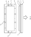
- Figure 1 shows in simplified schematic form an example of OLED device to which the invention can be applied.
- the OLED comprises a substrate 10 and a transparent conductive layer 12 over the substrate (transparent because this example is a bottom emitting structure).
- An encapsulated OLED structure is provided over the contact layer 12, comprising OLED layers 11 which are much thinner than the substrate, and an encapsulation 22.
- An outer ledge 16 of the contact layer 12 extends laterally beyond an outer edge of the encapsulated OLED structure.
- the OLED structure has multiple anode and cathode contacts, and these connect to different contact regions of the contact layer 12 in the ledge area to form contact areas for the cathode and anode layers of the OLED structure.
- the plan view in Figure 1 shows four cathode contact regions 12c, one at the center of each edge of the OLED structure, and four anode contact regions 12a at the four corners. Separation gaps 18 are provided.
- Figure 1 shows a bottom emitting OLED structure, with light emitted through the substrate.
- the contact layer 12 is transparent, and can for example comprise ITO, ZnO:Al, or other transparent conductors, typically materials from the group of transparent conductive oxides (TCOs). New technologies such as carbon nano-tubes or layer sequences can also be used.
- the relatively high resistance of some transparent conductors, such as ITO means that electrical connections with better conductivity are desired to distribute the current along the contact ledges to the anode contact regions and the cathode contact regions to reduce voltage drop and hence improve on homogeneity.
- a PCB in a frame shape can be mounted over the contact ledge 16.
- the structure is shown in more detail in Figure 2 , with the PCB 20 mounted on the contact ledge 16.
- ACF bonded anisotropic conductive film
- the structure of the OLED device can be conventional.
- a typical OLED according to the state of the art consists of active organic layers, a cathode, an anode, and a substrate.
- the active organic layers consist of a hole transport layer and a light emitting polymer for a polymer-based OLED (known as p-OLEDs).
- the small-molecule version of an OLED (known as sm-OLEDs) consists of some additional layers: hole injecting, emitting, hole blocking and electron transport layers.
- functional layers like CGL (charge generation layers) can also be included.
- the manufacture of the OLED can be based on printed or evaporated OLEDs but also other/future techniques like liquid processing can be used.
- additional encapsulation thin film layers 22 are deposited on this stack, as mentioned above, to protect the organic material from e.g. water and oxygen to prevent early degradation of the OLED materials.
- This protection is called thin film encapsulation (TFE), because the layer or layers have a thickness of about 100nm.
- the thin film encapsulation layer can consist of inorganic oxides, such as AI2 O3 or alternating layers of of AI2 O3 and ZrO2 , called a nanolaminate structure, deposited for example by atomic layer deposition (ALD).
- These encapsulation thin film layers are dielectric and insulating.
- the OLED active layers are deposited on a substrate which may be coated with, for instance, indium tin oxide (ITO), thereby forming an ITO layer typically of about 150 nm to function as a hole-injecting electrode.
- ITO indium tin oxide
- the cathode applied on top of the organic layers which provides electron injection is of the order of 100 nm thick.
- the OLED layer stack 11 is provided between the anode layer 12 and the encapsulation 22.
- the contact layer 12 functions as the anode, and the layer stack 11 then comprises the organic layers and a top cathode metal.
- the layer stack 11 may include the anode layer (in addition to the contact layer).
- the substrate 10 is the substrate for the OLED stack.
- the substrate can be glass for rigid devices or it may be plastic (typically with a barrier layer) for example for flexible devices. Very thin glass substrates can also enable a degree of bending.
- the encapsulation 22 overlaps the edge of the OLED layers 11 but terminates before the contact ledge 16, whereas the contact layer 12 extends fully to the outer edge so that the PCB 20 can connect to the contact regions.
- An alternative is to extend the encapsulation layers (in case of thin film encapsulation rather than glass encapsulation) to the edge of the device which is then locally removed in regions where contact with the underlying electrodes is desired.
- the cathode layer can be sufficiently conductive to provide homogeneous devices of relevant dimensions.
- a metal foil 14 may also be provided over the top for heat distribution/dissipation and mechanical protection of the thin film encapsulation.
- An adhesive layer 15 bonds the metal foil (if present) to the encapsulation 22.
- the ledge width can be of the order of 3mm
- the overall device thickness can be approximately 1mm to 3mm based on a rigid glass substrate thickness typically in the range 0.7 to 2.0mm. Thinner devices may be formed using bendable glass substrates or flexible plastics substrates.
- the overall panel size can have typical linear dimensions in the range 5cm to 30cm, although larger or smaller devices are possible.
- the PCB 20 is glued to the OLED and hence is part of the module which is generally sold separately from the driver electronics.
- the PCB is not removable from the device substrate.
- the driver electronics is then wired to the PCB.
- FIG. 2 shows schematically the driver 25 coupled to the PCB 20 by a flat cable 26, although a plug and socket can be used.
- This interconnection between the LED-PCB module and the driver can be located at a different place to the OLED unit itself, for example set aside in a luminaire housing or in a piece of furniture.
- the driver 25 includes testing circuitry 27, described further below.
- the combination of driver 25 and OLED module may change throughout the lifetime of an OLED, whereas the combination of an OLED and its associated PCB will not.
- the printed circuit board 20 has a bottom metallization layer which includes pads for connecting to the anode and cathode regions 12a, 12c. Conductive glue can be used to bond these pads to the cathode and anode contact regions of the connection layer.
- the PCB has a second metallization layer for providing interconnects between the anode regions and between the cathode regions. It might comprise even more layers in case more complex contacting structures are used, for example as may be required for color tunable devices. Thus, the PCB comprises at least two conducting layers. Vias are used to connect between the layers at desired locations.
- the second layer can be at the top or within the PCB structure.
- the PCB has a frame shape mounted over the outer ledge 16. In addition to interconnecting the cathode and anode regions, it provides the external contacts for electrical connection of the driver to the OLED as shown in Figure 2 .
- Other shapes of the PCB can be used, or a number of smaller more local PCBs can be used to contact the cathode/anode layers if the device design allows for it.
- Figure 2 also shows a light diffusing foil 24 at the light output face of the OLED package. This may or may not be desired depending on the lighting application.
- the invention makes use of a capacitive encoding structure formed within, or on top of, the stack of layers which define the OLED.
- the capacitor arrangement makes use of existing layers within the structure of the OLED.
- the capacitor arrangement makes use of the thin film encapsulation 22, deposited on the cathode side of the OLED.
- the anode side is then protected by the carrier material directly in the case of a glass substrate or via further layers in the case of a plastic substrate.
- the addition of a capacitor electrode, for example as part of an extended thin film encapsulation, implements a dedicated integrated capacitor structure to provide information about the size and type of the OLED device.
- FIG. 3 shows the structure used to form a capacitance.
- the OLED structure is shown as the active layer structure 34 and a top cathode 36.
- the contact layer 12 functions as the anode.
- the encapsulation layer 22 typically has a thickness of about 100nm.
- the capacitor electrode layer 40 may consist of any metal or transparent conducting oxide.
- the deposition process can be vacuum evaporation, sputtering, plasma enhanced laser deposition (PLD), or ALD.
- the cathode 36 couples down to a cathode contact portion 37 of the metal layer which forms the anode 12.
- the capacitor electrode may be formed by the heat spreader 14 shown in Figure 2 if it is an electrically conducting layer. This, in this case, the capacitor can be formed with no additional layers.
- the encapsulation layer 22 and the adhesive layer 15 then together function as the capacitor dielectric.
- the layer 40 in Figure 3 may be an additional metal layer over the encapsulation when there is no conductive heat spreader layer present, or else the layer 40 may comprise (or perform the additional function of) a heat spreader layer.
- an additional heat spreading layer may be provided over the top of the structure shown in Figure 3 .
- the use of separate heat spreading and capacitor electrode layers enables them to be optimized for their respective functions (i.e. thermal conductivity vs. electrical conductivity).
- the conductive layer 40 forms a top capacitor electrode pad and defines the second electrode of a capacitor having its first electrode formed by the underlying cathode layer 36.
- the capacitor and OLED are in series between the anode contact 32 and the capacitor electrode 40.
- the capacitor electrode 40 is formed so that it can be electrically contacted on the same side of the substrate as the anode and cathode areas 12,36 of the OLED device.
- the capacitor electrode 40 may be deposited over the complete OLED area (although leaving exposed contact areas for the anode and cathode 12,36).
- the effective area of the capacitor formed is shown by shape 42 which corresponds to the emission area.
- the capacitive value C is indicative of the area of the OLED device. This is schematically indicated in Figure 6 for various OLED sizes. Each of the three examples is based on the structure of Figure 5 , but scaled to a different size and shape.
- FIG. 7 A circuit arrangement to realize this automatic current adaption is shown in Figure 7 .
- This figure shows the OLED device 70 with anode and cathode terminals 12, 36 and an additional terminal 72 for the capacitive structure 74.
- a power supply 76 is coupled to the OLED device via the terminals 12,36.
- Additional circuitry 78 is coupled to the additional terminal 72. This additional circuit is used to determine the capacitive value of the structure 74 and generates an output signal which determines the operating current of power source fed into the OLED device.
- the operating current for the OLED is determined according to a sequence as set out below:
- the power supply is coupled to the OLED. This assumes an initial state in which the OLED device is unpowered and the capacitive structure is discharged.
- the power supply is turned on which triggers the capacitance detector to determine the capacitance value of the capacitive structure 74 as a third step.
- the capacitance value is converted into a signal proportional to the capacitance.
- the current of the power source is adjusted depending on the signal proportional to the capacitance.
- the adjusted current is fed into the connected OLED device.
- Figure 8 shows an alternative in which the capacitor electrode layer 40 only covers a portion of the emission layer.
- the layer has a strip shape with length L and width W.
- the effective length Leff is the length which overlaps with the cathode area 36.
- this capacitance value will vary in dependence on the nature of the encapsulation layer, in particular the thickness of the layer. This thickness may vary between different OLED designs. For example if a design is scaled up in size, the encapsulation may be scaled in thickness as well as in overall area. These differences in the nature of the encapsulation can be taken into account by the driver, by providing additional information to the driver concerning the nature of the encapsulation used in the particular OLED design.
- An alternative approach is to make use of an additional reference capacitor of fixed size.
- a pair of capacitor electrodes may be used.
- One electrode defines a readout capacitor and another electrode defines a reference capacitor.
- the reference capacitor has a fixed size, whereas the readout capacitor scales with the OLED design.
- the relative area of the reference and readout capacitor is used to encodes information concerning the electrical characteristics of the LED component.
- 1 cm 2 of the OLED area may be used as the reference capacitor, and a fixed proportion (90% or 50% for example) of the remaining area is used to for the readout capacitor.
- a fixed proportion (90% or 50% for example) of the remaining area is used to for the readout capacitor.
- one of the capacitors scales if the design is scaled, whereas the other stays a constant size.
- the ratio of the areas between the two capacitors is then used to encode the required driver current.
- the ratio between the capacitance values associated with the electrodes 90a and 90b is used.
- the capacitor electrode is formed as two portions comprising a variable size portion 40a which has an area which is a fixed proportion of the area of the OLED stack and a fixed size portion 40b. Each has its own respective readout terminal 100, 102.
- the capacitive structure is now divided into two parts. Two capacitors are defined in parallel, formed by separating he capacitor layer into two the portions 40a, 40b.
- the area 40a is proportion to the active area 42 of the OLED while the area 40b is constant.
- the area Aa is proportional to the emission area whereas Ab is constant, so that the ratio rC is proportional to the emission area. This ratio can thus be used to adjust the driving current for example to achieve a constant brightness for a range of OLED devices having different areas.
- Figure 10 shows the electrical circuit formed by the two capacitors, which are formed in parallel with the OLED.
- Figure 11 shows how the design of Figure 9 is scaled to different OLED sizes.
- the electrode 40a scales whereas the electrode 40b does not.
- the size of the two portions of the electrode layer may be freely chosen as long as the required proportionality between the capacitance ratio and the emission area size is maintained for the whole range of differently sized OLEDs.
- it is not essential that the reference capacitor has a constant size for all OLED designs.
- a range of OLEDs of a certain design type may be designed with emission areas of 1.0, 1.5 .... 9.5, 10 times a reference area A 0 .
- the reference area may not be constant.
- the larger capacitor may reach a maximum size after which the reference electrode is reduced in size to achieve the desired ratio.
- the advantage of the capacitance ratio approach is that the ratio is independent of the thickness th and permittivity eps, so that variations, for example due to production tolerances, are cancelled out.
- the circuit arrangement has to be modified so that two capacitive values can be measured and a controlling signal has to be generated which is proportional to the ratio of the two capacitance values Ca and Cb.
- This can for example be achieved by using a basic capacitive detector and carrying out the measurements time-sequentially to determine both capacitive values.
- the additional circuitry 78 is coupled to the two additional terminals 100, 102 in time sequential manner.
- the operating current for the OLED is determined according to a sequence as set out below:
- the power supply is coupled to the OLED. This assumes an initial state in which the OLED device is unpowered and the capacitive structure is discharged.
- the power supply is turned on. This triggers the capacitance detector to determine the readout capacitance value Ca in a third step and to determine the reference capacitance Cb as fourth step.
- the circuit delivers a signal dependent on the ratio Ca/Cb.
- the current of the power source is adjusted depending on the signal dependent on the capacitance ratio.
- the adjusted current is fed into the connected OLED device.
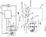
- a detection circuit may instead be used which measures the capacitance ratio directly a shown in Figure 13 .
- the readout circuit 140 comprises a current source 142 which drives a reference current Iref through the reference capacitor Cb. The resulting voltage is fed by a buffer 144 with gain g to one input of a differential measurement amplifier 146. The other input of the differential measurement amplifier is provided with the voltage on the readout capacitor Ca, and the difference between them is defined in Figure 13 as Vin. This voltage is applied across a shunt resistor 148 with resistance RSH.
- i Cb Cb * dU Cb / dt
- i Ca Ca * dU Ca / dt
- I Cb is set by the circuit as Iref.
- Vout RSH * Ca / Cb * g * Iref
- This output voltage Vout is the circuit output and is proportional to the capacitance ratio (and this remains the case if the amplifier 146 has a non-unity gain).
- a set of devices of different sizes can be made to the same but scaled design.
- the scaling automatically alters the capacitance value as a result of the change in layer area. Again, the scaling does not alter the layer thicknesses, so it is in two dimensions.
- the capacitance can be measured utilizing other circuits will will be well known to those skilled in the art.
- the invention can be applied to all types of LED devices which generate output over an area of a layer, in particular OLED devices. It is of particular interest for general lighting applications and OLED based luminaires.
- the encoded information can relate to a light output panel with a single output area which has controllable brightness and/or color.
Landscapes
- Physics & Mathematics (AREA)
- Optics & Photonics (AREA)
- General Physics & Mathematics (AREA)
- Electroluminescent Light Sources (AREA)
Claims (10)
- OLED-Vorrichtung, umfassend:ein Substrat (10);eine transparente leitfähige Anodenschicht (12) auf dem Substrat (10);einen Stapel von Schichten (11) auf der Anodenschicht (12), die eine OLED-Komponente mit einer Emissionsfläche (42) bilden,wobei der Stapel von Schichten (11) eine elektrolumineszente Schicht (34) und eine obere Kathodenschicht (36) umfasst, unddie OLED-Komponente elektrischen Eigenschaften aufweist,dadurch gekennzeichnet, dassder Stapel von Schichten (11) ferner eine auf der Kathodenschicht (36) aufgebrachte Verkapselungsschicht (22) zum Schutz der OLED-Komponente umfasst;wobei die OLED-Vorrichtung ferner eine kapazitive Kodierungsstruktur (36, 22, 40, 74) umfasst, die eine Kondensatorelektrodenschicht (40) umfasst, die auf der Verkapselungsschicht (22) ausgebildet ist,wobei die Verkapselungsschicht (22) eine dielektrische Kondensatorschicht zwischen der darunter liegenden Kathodenschicht (36) und der darüber liegenden Kondensatorelektrodenschicht (40) bildet,wobei die Fläche der Kondensatorelektrodenschicht (40) eine Kapazität definiert,wobei die Kapazität Information über die elektrischen Eigenschaften der OLED-Komponente kodiert; undwobei die Fläche der Kondensatorelektrodenschicht (40) in einem vorbestimmten Verhältnis zur Emissionsfläche (42) der OLED-Komponente steht.
- OLED-Vorrichtung nach Anspruch 1, wobei die Kondensatorelektrodenschicht (40) in zwei Teile geteilt ist, wobei einer der Teile eine Referenzkondensatorelektrode (40b) bildet, die eine Referenzkapazität zwischen der Referenzkondensatorelektrode (40b) und der Kathodenschicht (36) definiert, und der andere Teil eine Auslesekondensatorelektrode (40a) bildet, die eine Auslesekapazität zwischen der Auslesekondensatorelektrode (40a) und der Kathodenschicht (36) definiert, wobei ein Verhältnis zwischen der Referenzkapazität und der Auslesekapazität die Information über die elektrischen Eigenschaften der OLED-Komponente kodiert.
- OLED-Vorrichtung nach Anspruch 2, wobei die Referenzkondensatorelektrode (40b) eine feste Fläche hat und die Auslesekondensatorelektrode (40a) mit der Emissionsfläche (42) der OLED-Komponente skaliert.
- OLED-Vorrichtung nach einem der vorhergehenden Ansprüche, wobei sich die elektrischen Eigenschaften auf einen gewünschten Treiberstrom und/oder eine gewünschte Spannung und/oder einen erforderlichen Dimmwert der OLED-Komponente beziehen.
- OLED-Vorrichtung nach einem der vorhergehenden Ansprüche, wobei die Kondensatorelektrodenschicht eine wärmeausbreitende Schicht (14) umfasst, wobei die Verkapselungsschicht (22) in Kombination mit einer wärmeausbreitenden Klebstoffschicht (15) den dielektrischen Kondensator definiert.
- OLED-Vorrichtung nach einem der Ansprüche 1 bis 5, die ferner eine wärmeverteilende Schicht über der Kondensatorelektrodenschicht (40) umfasst.
- Satz von OLED-Vorrichtungen, der ein Vielfaches der OLED-Vorrichtung nach Anspruch 1 umfasst, wobei die Fläche der Kondensatorelektrodenschicht (40) jeder der jeweiligen OLED-Vorrichtungen ein vorbestimmtes Verhältnis zur Emissionsfläche (42) der jeweiligen OLED-Vorrichtung ist.
- OLED-Beleuchtungsvorrichtung, die umfasst:
eine OLED-Vorrichtung nach Anspruch 1, ferner mit Anschlüssen an der Anodenschicht (12) und der Kathodenschicht (36), die mit einer Stromversorgung (76) gekoppelt sind, und einem zusätzlichen Anschluss (72), der mit der kapazitiven Kodierungsstruktur (36, 22, 40, 74) verbunden ist; einer Leiterplatte (20), die mit den Anschlüssen (12, 36, 72) der OLED-Vorrichtung verbunden ist; und einen Treiber (25), der einen Verbindungsteil zum Verbinden mit der PCB (20) umfasst, wobei der Treiber eine Testschaltung (27, 78) umfasst, die mit dem zusätzlichen Anschluss (72) gekoppelt ist, um die Kapazität der kapazitiven Kodierungsstruktur (36, 22, 40, 74) zu bestimmen. - OLED-Beleuchtungsvorrichtung nach Anspruch 8, wobei der Treiber (25) so beschaffen ist, dass er die OLED-Vorrichtung in Abhängigkeit von der kodierten Information über die elektrischen Eigenschaften der OLED-Komponente, wie sie von der Testschaltung (27) ermittelt wurden, ansteuert.
- Verfahren zur Ansteuerung einer OLED-Beleuchtungsvorrichtung nach Anspruch 8, wobei das Verfahren umfasst:Bereitstellen der OLED-Vorrichtung in einem Ausgangszustand, in dem die OLED-Komponente nicht mit Strom versorgt wird und die kapazitive Kodierungsstruktur (36, 22, 40, 74) entladen ist;Bereitstellen einer Stromversorgung (76), die mit der OLED-Komponent zwischen den Anschlüssen für die Anodenschicht (12) und die Kathodenschicht (36) und zwischen der Kathodenschicht (36) und dem Anschluss für die Kondensatorelektrodenschicht (72) der kapazitive Kodierungsstruktur gekoppelt ist und einen Betriebsstrom liefert;Bestimmung eines Kapazitätswerts der kapazitive Kodierungsstruktur (36, 22, 40, 74);Umwandlung des Kapazitätswertes in ein zur Kapazität proportionales Signal;Einstellen des Stroms der Stromversorgung in Abhängigkeit von dem zum Kapazitätswert proportionalen Signal; undEinspeisung des eingestellten Stroms in die OLED-Komponente.
Priority Applications (3)
| Application Number | Priority Date | Filing Date | Title |
|---|---|---|---|
| EP15161668.7A EP3076757B1 (de) | 2015-03-30 | 2015-03-30 | Oled-vorrichtung und ansteuerungsverfahren |
| PCT/EP2016/056884 WO2016156373A1 (en) | 2015-03-30 | 2016-03-30 | Led device, led driver, and driving method |
| US15/554,323 US10165649B2 (en) | 2015-03-30 | 2016-03-30 | LED device, LED driver, and driving method |
Applications Claiming Priority (1)
| Application Number | Priority Date | Filing Date | Title |
|---|---|---|---|
| EP15161668.7A EP3076757B1 (de) | 2015-03-30 | 2015-03-30 | Oled-vorrichtung und ansteuerungsverfahren |
Publications (2)
| Publication Number | Publication Date |
|---|---|
| EP3076757A1 EP3076757A1 (de) | 2016-10-05 |
| EP3076757B1 true EP3076757B1 (de) | 2023-01-04 |
Family
ID=52875517
Family Applications (1)
| Application Number | Title | Priority Date | Filing Date |
|---|---|---|---|
| EP15161668.7A Active EP3076757B1 (de) | 2015-03-30 | 2015-03-30 | Oled-vorrichtung und ansteuerungsverfahren |
Country Status (3)
| Country | Link |
|---|---|
| US (1) | US10165649B2 (de) |
| EP (1) | EP3076757B1 (de) |
| WO (1) | WO2016156373A1 (de) |
Families Citing this family (4)
| Publication number | Priority date | Publication date | Assignee | Title |
|---|---|---|---|---|
| EP3076757B1 (de) | 2015-03-30 | 2023-01-04 | OLEDWorks GmbH | Oled-vorrichtung und ansteuerungsverfahren |
| WO2018236767A2 (en) * | 2017-06-20 | 2018-12-27 | Tesoro Scientific, Inc. | Light emitting diode (led) test apparatus and method of manufacture |
| KR102518747B1 (ko) * | 2017-12-28 | 2023-04-07 | 삼성디스플레이 주식회사 | 유기전계발광 표시장치 및 그의 구동방법 |
| CN111009618A (zh) | 2019-12-18 | 2020-04-14 | 固安翌光科技有限公司 | 一种有机电致发光器件 |
Citations (3)
| Publication number | Priority date | Publication date | Assignee | Title |
|---|---|---|---|---|
| WO2010092504A1 (en) * | 2009-02-12 | 2010-08-19 | Philips Intellectual Property & Standards Gmbh | Light emitting device system and driver |
| EP2595210A2 (de) * | 2011-11-21 | 2013-05-22 | Panasonic Corporation | Organisches EL-Beleuchtungsmodul und Beleuchtungsvorrichtung damit |
| DE102013109814A1 (de) * | 2013-09-09 | 2015-03-12 | Osram Oled Gmbh | Optoelektronisches Bauelement, optoelektronische Bauelementevorrichtung und Verfahren zum Herstellen eines optoelektronischen Bauelementes |
Family Cites Families (19)
| Publication number | Priority date | Publication date | Assignee | Title |
|---|---|---|---|---|
| DE10042500A1 (de) * | 2000-08-30 | 2002-03-14 | Kostal Leopold Gmbh & Co Kg | Elektrolumineszenz-Display |
| US20070029939A1 (en) * | 2005-08-05 | 2007-02-08 | Philip Burkum | Electroluminescent sign having a coded information region |
| KR101315088B1 (ko) | 2005-10-20 | 2013-10-07 | 코닌클리케 필립스 엔.브이. | 조명 장치 |
| CN101652669B (zh) * | 2007-03-30 | 2013-06-19 | 皇家飞利浦电子股份有限公司 | 用于确定led/oled设备的状态和/或条件的方法以及诊断设备 |
| EP2208393B1 (de) * | 2007-11-01 | 2019-04-24 | Nxp B.V. | Led-paket und verfahren zur herstellung eines solchen led-pakets |
| US8508136B2 (en) * | 2008-09-09 | 2013-08-13 | Koninklijke Philips N.V. | OLED lighting device with tag element |
| CN102165844B (zh) | 2008-09-25 | 2014-01-08 | 赤多尼科两合股份有限公司 | 发光装置的操作装置和方法 |
| WO2010125493A1 (en) | 2009-04-23 | 2010-11-04 | Koninklijke Philips Electronics N. V. | Segmented electroluminescent device with resistive interconnect layers |
| US20130082997A1 (en) | 2011-09-30 | 2013-04-04 | Apple Inc. | System and method for detection of dimensions of display panel or other patterned device |
| US9312314B2 (en) | 2012-02-02 | 2016-04-12 | Koninklijke Philips N.V. | Light apparatus for generating light |
| RU2014140547A (ru) * | 2012-03-08 | 2016-04-27 | Конинклейке Филипс Н.В. | Сегментированное электролюминесцентное устройство с элементами распределенной нагрузки |
| FR2994301B1 (fr) * | 2012-07-31 | 2014-10-17 | Stephane Blondeau | Authentification de personne par biometrie |
| KR102111560B1 (ko) | 2013-07-12 | 2020-05-18 | 삼성디스플레이 주식회사 | 유기발광표시장치 및 그 제조방법 |
| US10042504B2 (en) * | 2013-08-13 | 2018-08-07 | Samsung Electronics Company, Ltd. | Interaction sensing |
| AT14906U1 (de) * | 2013-11-28 | 2016-08-15 | Tridonic Gmbh & Co Kg | LED-Modul |
| WO2015135889A1 (en) * | 2014-03-13 | 2015-09-17 | Koninklijke Philips N.V. | Electronic device, device driver, and driving method |
| EP3547493B1 (de) * | 2014-03-26 | 2020-05-20 | Tridonic GmbH & Co. KG | Beleuchtungssystem und verfahren für einen notlichtbetrieb |
| EP3076757B1 (de) | 2015-03-30 | 2023-01-04 | OLEDWorks GmbH | Oled-vorrichtung und ansteuerungsverfahren |
| EP3076756B1 (de) | 2015-03-30 | 2021-07-21 | OLEDWorks GmbH | Oled-vorrichtung und ansteuerungsverfahren |
-
2015
- 2015-03-30 EP EP15161668.7A patent/EP3076757B1/de active Active
-
2016
- 2016-03-30 US US15/554,323 patent/US10165649B2/en active Active
- 2016-03-30 WO PCT/EP2016/056884 patent/WO2016156373A1/en not_active Ceased
Patent Citations (3)
| Publication number | Priority date | Publication date | Assignee | Title |
|---|---|---|---|---|
| WO2010092504A1 (en) * | 2009-02-12 | 2010-08-19 | Philips Intellectual Property & Standards Gmbh | Light emitting device system and driver |
| EP2595210A2 (de) * | 2011-11-21 | 2013-05-22 | Panasonic Corporation | Organisches EL-Beleuchtungsmodul und Beleuchtungsvorrichtung damit |
| DE102013109814A1 (de) * | 2013-09-09 | 2015-03-12 | Osram Oled Gmbh | Optoelektronisches Bauelement, optoelektronische Bauelementevorrichtung und Verfahren zum Herstellen eines optoelektronischen Bauelementes |
Also Published As
| Publication number | Publication date |
|---|---|
| US20180242425A1 (en) | 2018-08-23 |
| US10165649B2 (en) | 2018-12-25 |
| EP3076757A1 (de) | 2016-10-05 |
| WO2016156373A1 (en) | 2016-10-06 |
Similar Documents
| Publication | Publication Date | Title |
|---|---|---|
| JP5285056B2 (ja) | 有機発光ダイオードディスプレイ | |
| US8508136B2 (en) | OLED lighting device with tag element | |
| US10165649B2 (en) | LED device, LED driver, and driving method | |
| US20090267523A1 (en) | Driver circuit for light sheet module with direct connection to power source | |
| JP2013502620A5 (de) | ||
| WO2017115712A1 (ja) | 発光モジュール | |
| CN110690224A (zh) | 电子装置 | |
| US7071618B2 (en) | Electroluminescent element comprising electrically coupled shield layer | |
| US20120049725A1 (en) | Segmented electroluminescent device with resistive interconnect layers | |
| CN105980768A (zh) | 照明膜结构 | |
| JP2007227927A (ja) | 照明装置 | |
| EP3025383A1 (de) | Elektronische steuerung von oleds mit verteilten elektroden | |
| EP3117689B1 (de) | Elektronische vorrichtung, vorrichtungstreiber und ansteuerverfahren | |
| US9807834B2 (en) | Load device, driver for driving the load, and driving method | |
| EP2634474A1 (de) | Lichtemittierendes modul | |
| US9733753B2 (en) | Flat self-luminous touch switch | |
| EP3076756B1 (de) | Oled-vorrichtung und ansteuerungsverfahren | |
| CN117193571A (zh) | 显示面板及显示装置 | |
| US20250279020A1 (en) | Display Device | |
| US7518306B2 (en) | Light unit with staggered electrodes | |
| CN208572516U (zh) | 显示装置 | |
| KR101997687B1 (ko) | 봉지화된 전자소자의 제조방법 | |
| JP2000194274A (ja) | 発光装置 | |
| JP2016170963A (ja) | 発光装置 |
Legal Events
| Date | Code | Title | Description |
|---|---|---|---|
| PUAI | Public reference made under article 153(3) epc to a published international application that has entered the european phase |
Free format text: ORIGINAL CODE: 0009012 |
|
| AK | Designated contracting states |
Kind code of ref document: A1 Designated state(s): AL AT BE BG CH CY CZ DE DK EE ES FI FR GB GR HR HU IE IS IT LI LT LU LV MC MK MT NL NO PL PT RO RS SE SI SK SM TR |
|
| AX | Request for extension of the european patent |
Extension state: BA ME |
|
| STAA | Information on the status of an ep patent application or granted ep patent |
Free format text: STATUS: REQUEST FOR EXAMINATION WAS MADE |
|
| 17P | Request for examination filed |
Effective date: 20170222 |
|
| RBV | Designated contracting states (corrected) |
Designated state(s): AL AT BE BG CH CY CZ DE DK EE ES FI FR GB GR HR HU IE IS IT LI LT LU LV MC MK MT NL NO PL PT RO RS SE SI SK SM TR |
|
| STAA | Information on the status of an ep patent application or granted ep patent |
Free format text: STATUS: EXAMINATION IS IN PROGRESS |
|
| 17Q | First examination report despatched |
Effective date: 20191209 |
|
| REG | Reference to a national code |
Ref country code: DE Ref legal event code: R079 Ref document number: 602015082147 Country of ref document: DE Free format text: PREVIOUS MAIN CLASS: H05B0033080000 Ipc: H05B0045140000 |
|
| GRAP | Despatch of communication of intention to grant a patent |
Free format text: ORIGINAL CODE: EPIDOSNIGR1 |
|
| STAA | Information on the status of an ep patent application or granted ep patent |
Free format text: STATUS: GRANT OF PATENT IS INTENDED |
|
| RIC1 | Information provided on ipc code assigned before grant |
Ipc: H05B 45/14 20200101AFI20220908BHEP |
|
| INTG | Intention to grant announced |
Effective date: 20220927 |
|
| GRAS | Grant fee paid |
Free format text: ORIGINAL CODE: EPIDOSNIGR3 |
|
| GRAA | (expected) grant |
Free format text: ORIGINAL CODE: 0009210 |
|
| STAA | Information on the status of an ep patent application or granted ep patent |
Free format text: STATUS: THE PATENT HAS BEEN GRANTED |
|
| AK | Designated contracting states |
Kind code of ref document: B1 Designated state(s): AL AT BE BG CH CY CZ DE DK EE ES FI FR GB GR HR HU IE IS IT LI LT LU LV MC MK MT NL NO PL PT RO RS SE SI SK SM TR |
|
| REG | Reference to a national code |
Ref country code: GB Ref legal event code: FG4D |
|
| REG | Reference to a national code |
Ref country code: DE Ref legal event code: R096 Ref document number: 602015082147 Country of ref document: DE |
|
| REG | Reference to a national code |
Ref country code: CH Ref legal event code: EP |
|
| REG | Reference to a national code |
Ref country code: AT Ref legal event code: REF Ref document number: 1542819 Country of ref document: AT Kind code of ref document: T Effective date: 20230115 |
|
| REG | Reference to a national code |
Ref country code: IE Ref legal event code: FG4D |
|
| REG | Reference to a national code |
Ref country code: LT Ref legal event code: MG9D |
|
| REG | Reference to a national code |
Ref country code: NL Ref legal event code: MP Effective date: 20230104 |
|
| REG | Reference to a national code |
Ref country code: AT Ref legal event code: MK05 Ref document number: 1542819 Country of ref document: AT Kind code of ref document: T Effective date: 20230104 |
|
| PG25 | Lapsed in a contracting state [announced via postgrant information from national office to epo] |
Ref country code: NL Free format text: LAPSE BECAUSE OF FAILURE TO SUBMIT A TRANSLATION OF THE DESCRIPTION OR TO PAY THE FEE WITHIN THE PRESCRIBED TIME-LIMIT Effective date: 20230104 |
|
| REG | Reference to a national code |
Ref country code: GB Ref legal event code: 732E Free format text: REGISTERED BETWEEN 20230629 AND 20230705 |
|
| PG25 | Lapsed in a contracting state [announced via postgrant information from national office to epo] |
Ref country code: RS Free format text: LAPSE BECAUSE OF FAILURE TO SUBMIT A TRANSLATION OF THE DESCRIPTION OR TO PAY THE FEE WITHIN THE PRESCRIBED TIME-LIMIT Effective date: 20230104 Ref country code: PT Free format text: LAPSE BECAUSE OF FAILURE TO SUBMIT A TRANSLATION OF THE DESCRIPTION OR TO PAY THE FEE WITHIN THE PRESCRIBED TIME-LIMIT Effective date: 20230504 Ref country code: NO Free format text: LAPSE BECAUSE OF FAILURE TO SUBMIT A TRANSLATION OF THE DESCRIPTION OR TO PAY THE FEE WITHIN THE PRESCRIBED TIME-LIMIT Effective date: 20230404 Ref country code: LV Free format text: LAPSE BECAUSE OF FAILURE TO SUBMIT A TRANSLATION OF THE DESCRIPTION OR TO PAY THE FEE WITHIN THE PRESCRIBED TIME-LIMIT Effective date: 20230104 Ref country code: LT Free format text: LAPSE BECAUSE OF FAILURE TO SUBMIT A TRANSLATION OF THE DESCRIPTION OR TO PAY THE FEE WITHIN THE PRESCRIBED TIME-LIMIT Effective date: 20230104 Ref country code: HR Free format text: LAPSE BECAUSE OF FAILURE TO SUBMIT A TRANSLATION OF THE DESCRIPTION OR TO PAY THE FEE WITHIN THE PRESCRIBED TIME-LIMIT Effective date: 20230104 Ref country code: ES Free format text: LAPSE BECAUSE OF FAILURE TO SUBMIT A TRANSLATION OF THE DESCRIPTION OR TO PAY THE FEE WITHIN THE PRESCRIBED TIME-LIMIT Effective date: 20230104 Ref country code: AT Free format text: LAPSE BECAUSE OF FAILURE TO SUBMIT A TRANSLATION OF THE DESCRIPTION OR TO PAY THE FEE WITHIN THE PRESCRIBED TIME-LIMIT Effective date: 20230104 |
|
| PG25 | Lapsed in a contracting state [announced via postgrant information from national office to epo] |
Ref country code: SE Free format text: LAPSE BECAUSE OF FAILURE TO SUBMIT A TRANSLATION OF THE DESCRIPTION OR TO PAY THE FEE WITHIN THE PRESCRIBED TIME-LIMIT Effective date: 20230104 Ref country code: PL Free format text: LAPSE BECAUSE OF FAILURE TO SUBMIT A TRANSLATION OF THE DESCRIPTION OR TO PAY THE FEE WITHIN THE PRESCRIBED TIME-LIMIT Effective date: 20230104 Ref country code: IS Free format text: LAPSE BECAUSE OF FAILURE TO SUBMIT A TRANSLATION OF THE DESCRIPTION OR TO PAY THE FEE WITHIN THE PRESCRIBED TIME-LIMIT Effective date: 20230504 Ref country code: GR Free format text: LAPSE BECAUSE OF FAILURE TO SUBMIT A TRANSLATION OF THE DESCRIPTION OR TO PAY THE FEE WITHIN THE PRESCRIBED TIME-LIMIT Effective date: 20230405 Ref country code: FI Free format text: LAPSE BECAUSE OF FAILURE TO SUBMIT A TRANSLATION OF THE DESCRIPTION OR TO PAY THE FEE WITHIN THE PRESCRIBED TIME-LIMIT Effective date: 20230104 |
|
| REG | Reference to a national code |
Ref country code: DE Ref legal event code: R097 Ref document number: 602015082147 Country of ref document: DE |
|
| PG25 | Lapsed in a contracting state [announced via postgrant information from national office to epo] |
Ref country code: SM Free format text: LAPSE BECAUSE OF FAILURE TO SUBMIT A TRANSLATION OF THE DESCRIPTION OR TO PAY THE FEE WITHIN THE PRESCRIBED TIME-LIMIT Effective date: 20230104 Ref country code: RO Free format text: LAPSE BECAUSE OF FAILURE TO SUBMIT A TRANSLATION OF THE DESCRIPTION OR TO PAY THE FEE WITHIN THE PRESCRIBED TIME-LIMIT Effective date: 20230104 Ref country code: MC Free format text: LAPSE BECAUSE OF FAILURE TO SUBMIT A TRANSLATION OF THE DESCRIPTION OR TO PAY THE FEE WITHIN THE PRESCRIBED TIME-LIMIT Effective date: 20230104 Ref country code: EE Free format text: LAPSE BECAUSE OF FAILURE TO SUBMIT A TRANSLATION OF THE DESCRIPTION OR TO PAY THE FEE WITHIN THE PRESCRIBED TIME-LIMIT Effective date: 20230104 Ref country code: DK Free format text: LAPSE BECAUSE OF FAILURE TO SUBMIT A TRANSLATION OF THE DESCRIPTION OR TO PAY THE FEE WITHIN THE PRESCRIBED TIME-LIMIT Effective date: 20230104 Ref country code: CZ Free format text: LAPSE BECAUSE OF FAILURE TO SUBMIT A TRANSLATION OF THE DESCRIPTION OR TO PAY THE FEE WITHIN THE PRESCRIBED TIME-LIMIT Effective date: 20230104 |
|
| REG | Reference to a national code |
Ref country code: CH Ref legal event code: PL |
|
| PLBE | No opposition filed within time limit |
Free format text: ORIGINAL CODE: 0009261 |
|
| STAA | Information on the status of an ep patent application or granted ep patent |
Free format text: STATUS: NO OPPOSITION FILED WITHIN TIME LIMIT |
|
| PG25 | Lapsed in a contracting state [announced via postgrant information from national office to epo] |
Ref country code: SK Free format text: LAPSE BECAUSE OF FAILURE TO SUBMIT A TRANSLATION OF THE DESCRIPTION OR TO PAY THE FEE WITHIN THE PRESCRIBED TIME-LIMIT Effective date: 20230104 |
|
| REG | Reference to a national code |
Ref country code: BE Ref legal event code: MM Effective date: 20230331 |
|
| 26N | No opposition filed |
Effective date: 20231005 |
|
| PG25 | Lapsed in a contracting state [announced via postgrant information from national office to epo] |
Ref country code: LU Free format text: LAPSE BECAUSE OF NON-PAYMENT OF DUE FEES Effective date: 20230330 |
|
| REG | Reference to a national code |
Ref country code: IE Ref legal event code: MM4A |
|
| PG25 | Lapsed in a contracting state [announced via postgrant information from national office to epo] |
Ref country code: SI Free format text: LAPSE BECAUSE OF FAILURE TO SUBMIT A TRANSLATION OF THE DESCRIPTION OR TO PAY THE FEE WITHIN THE PRESCRIBED TIME-LIMIT Effective date: 20230104 Ref country code: LI Free format text: LAPSE BECAUSE OF NON-PAYMENT OF DUE FEES Effective date: 20230331 Ref country code: IE Free format text: LAPSE BECAUSE OF NON-PAYMENT OF DUE FEES Effective date: 20230330 Ref country code: CH Free format text: LAPSE BECAUSE OF NON-PAYMENT OF DUE FEES Effective date: 20230331 |
|
| PG25 | Lapsed in a contracting state [announced via postgrant information from national office to epo] |
Ref country code: BE Free format text: LAPSE BECAUSE OF NON-PAYMENT OF DUE FEES Effective date: 20230331 |
|
| PG25 | Lapsed in a contracting state [announced via postgrant information from national office to epo] |
Ref country code: IT Free format text: LAPSE BECAUSE OF FAILURE TO SUBMIT A TRANSLATION OF THE DESCRIPTION OR TO PAY THE FEE WITHIN THE PRESCRIBED TIME-LIMIT Effective date: 20230104 |
|
| PG25 | Lapsed in a contracting state [announced via postgrant information from national office to epo] |
Ref country code: BG Free format text: LAPSE BECAUSE OF FAILURE TO SUBMIT A TRANSLATION OF THE DESCRIPTION OR TO PAY THE FEE WITHIN THE PRESCRIBED TIME-LIMIT Effective date: 20230104 |
|
| PG25 | Lapsed in a contracting state [announced via postgrant information from national office to epo] |
Ref country code: BG Free format text: LAPSE BECAUSE OF FAILURE TO SUBMIT A TRANSLATION OF THE DESCRIPTION OR TO PAY THE FEE WITHIN THE PRESCRIBED TIME-LIMIT Effective date: 20230104 |
|
| PG25 | Lapsed in a contracting state [announced via postgrant information from national office to epo] |
Ref country code: CY Free format text: LAPSE BECAUSE OF FAILURE TO SUBMIT A TRANSLATION OF THE DESCRIPTION OR TO PAY THE FEE WITHIN THE PRESCRIBED TIME-LIMIT; INVALID AB INITIO Effective date: 20150330 |
|
| PG25 | Lapsed in a contracting state [announced via postgrant information from national office to epo] |
Ref country code: HU Free format text: LAPSE BECAUSE OF FAILURE TO SUBMIT A TRANSLATION OF THE DESCRIPTION OR TO PAY THE FEE WITHIN THE PRESCRIBED TIME-LIMIT; INVALID AB INITIO Effective date: 20150330 |
|
| PG25 | Lapsed in a contracting state [announced via postgrant information from national office to epo] |
Ref country code: TR Free format text: LAPSE BECAUSE OF FAILURE TO SUBMIT A TRANSLATION OF THE DESCRIPTION OR TO PAY THE FEE WITHIN THE PRESCRIBED TIME-LIMIT Effective date: 20230104 |
|
| PGFP | Annual fee paid to national office [announced via postgrant information from national office to epo] |
Ref country code: FR Payment date: 20251231 Year of fee payment: 12 |
|
| PGFP | Annual fee paid to national office [announced via postgrant information from national office to epo] |
Ref country code: GB Payment date: 20260106 Year of fee payment: 12 |
|
| PGFP | Annual fee paid to national office [announced via postgrant information from national office to epo] |
Ref country code: DE Payment date: 20260102 Year of fee payment: 12 |