EP3086361A2 - Procede de fabrication d'un agencement de substrat avec un moyen de pre-fixation, agencement de substrat correspondant, procede de connexion d'un composant electronique avec un agencement de substrat utiilisant un moyen de pre-fixation forme sur le composant electronique et/ou l'agencement de substrat et composant electronique connecte avec un agencement de substrat - Google Patents
Procede de fabrication d'un agencement de substrat avec un moyen de pre-fixation, agencement de substrat correspondant, procede de connexion d'un composant electronique avec un agencement de substrat utiilisant un moyen de pre-fixation forme sur le composant electronique et/ou l'agencement de substrat et composant electronique connecte avec un agencement de substrat Download PDFInfo
- Publication number
- EP3086361A2 EP3086361A2 EP16161902.8A EP16161902A EP3086361A2 EP 3086361 A2 EP3086361 A2 EP 3086361A2 EP 16161902 A EP16161902 A EP 16161902A EP 3086361 A2 EP3086361 A2 EP 3086361A2
- Authority
- EP
- European Patent Office
- Prior art keywords
- substrate
- electronic component
- prefixing
- agent
- arrangement
- Prior art date
- Legal status (The legal status is an assumption and is not a legal conclusion. Google has not performed a legal analysis and makes no representation as to the accuracy of the status listed.)
- Withdrawn
Links
Images



Classifications
-
- H—ELECTRICITY
- H10—SEMICONDUCTOR DEVICES; ELECTRIC SOLID-STATE DEVICES NOT OTHERWISE PROVIDED FOR
- H10P—GENERIC PROCESSES OR APPARATUS FOR THE MANUFACTURE OR TREATMENT OF DEVICES COVERED BY CLASS H10
- H10P72/00—Handling or holding of wafers, substrates or devices during manufacture or treatment thereof
- H10P72/70—Handling or holding of wafers, substrates or devices during manufacture or treatment thereof for supporting or gripping
- H10P72/74—Handling or holding of wafers, substrates or devices during manufacture or treatment thereof for supporting or gripping using temporarily an auxiliary support
- H10P72/7402—Wafer tapes, e.g. grinding or dicing support tapes
-
- H—ELECTRICITY
- H10—SEMICONDUCTOR DEVICES; ELECTRIC SOLID-STATE DEVICES NOT OTHERWISE PROVIDED FOR
- H10W—GENERIC PACKAGES, INTERCONNECTIONS, CONNECTORS OR OTHER CONSTRUCTIONAL DETAILS OF DEVICES COVERED BY CLASS H10
- H10W70/00—Package substrates; Interposers; Redistribution layers [RDL]
- H10W70/40—Leadframes
- H10W70/411—Chip-supporting parts, e.g. die pads
- H10W70/417—Bonding materials between chips and die pads
-
- H—ELECTRICITY
- H05—ELECTRIC TECHNIQUES NOT OTHERWISE PROVIDED FOR
- H05K—PRINTED CIRCUITS; CASINGS OR CONSTRUCTIONAL DETAILS OF ELECTRIC APPARATUS; MANUFACTURE OF ASSEMBLAGES OF ELECTRICAL COMPONENTS
- H05K2203/00—Indexing scheme relating to apparatus or processes for manufacturing printed circuits covered by H05K3/00
- H05K2203/11—Treatments characterised by their effect, e.g. heating, cooling, roughening
- H05K2203/1131—Sintering, i.e. fusing of metal particles to achieve or improve electrical conductivity
-
- H—ELECTRICITY
- H05—ELECTRIC TECHNIQUES NOT OTHERWISE PROVIDED FOR
- H05K—PRINTED CIRCUITS; CASINGS OR CONSTRUCTIONAL DETAILS OF ELECTRIC APPARATUS; MANUFACTURE OF ASSEMBLAGES OF ELECTRICAL COMPONENTS
- H05K3/00—Apparatus or processes for manufacturing printed circuits
- H05K3/30—Assembling printed circuits with electric components, e.g. with resistors
- H05K3/303—Assembling printed circuits with electric components, e.g. with resistors with surface mounted components
-
- H—ELECTRICITY
- H05—ELECTRIC TECHNIQUES NOT OTHERWISE PROVIDED FOR
- H05K—PRINTED CIRCUITS; CASINGS OR CONSTRUCTIONAL DETAILS OF ELECTRIC APPARATUS; MANUFACTURE OF ASSEMBLAGES OF ELECTRICAL COMPONENTS
- H05K3/00—Apparatus or processes for manufacturing printed circuits
- H05K3/30—Assembling printed circuits with electric components, e.g. with resistors
- H05K3/32—Assembling printed circuits with electric components, e.g. with resistors electrically connecting electric components or wires to printed circuits
-
- H—ELECTRICITY
- H05—ELECTRIC TECHNIQUES NOT OTHERWISE PROVIDED FOR
- H05K—PRINTED CIRCUITS; CASINGS OR CONSTRUCTIONAL DETAILS OF ELECTRIC APPARATUS; MANUFACTURE OF ASSEMBLAGES OF ELECTRICAL COMPONENTS
- H05K3/00—Apparatus or processes for manufacturing printed circuits
- H05K3/30—Assembling printed circuits with electric components, e.g. with resistors
- H05K3/32—Assembling printed circuits with electric components, e.g. with resistors electrically connecting electric components or wires to printed circuits
- H05K3/34—Assembling printed circuits with electric components, e.g. with resistors electrically connecting electric components or wires to printed circuits by soldering
-
- H—ELECTRICITY
- H10—SEMICONDUCTOR DEVICES; ELECTRIC SOLID-STATE DEVICES NOT OTHERWISE PROVIDED FOR
- H10P—GENERIC PROCESSES OR APPARATUS FOR THE MANUFACTURE OR TREATMENT OF DEVICES COVERED BY CLASS H10
- H10P72/00—Handling or holding of wafers, substrates or devices during manufacture or treatment thereof
- H10P72/70—Handling or holding of wafers, substrates or devices during manufacture or treatment thereof for supporting or gripping
- H10P72/74—Handling or holding of wafers, substrates or devices during manufacture or treatment thereof for supporting or gripping using temporarily an auxiliary support
- H10P72/7434—Handling or holding of wafers, substrates or devices during manufacture or treatment thereof for supporting or gripping using temporarily an auxiliary support used in a transfer process involving at least two transfer steps, i.e. including an intermediate handle substrate
-
- H—ELECTRICITY
- H10—SEMICONDUCTOR DEVICES; ELECTRIC SOLID-STATE DEVICES NOT OTHERWISE PROVIDED FOR
- H10W—GENERIC PACKAGES, INTERCONNECTIONS, CONNECTORS OR OTHER CONSTRUCTIONAL DETAILS OF DEVICES COVERED BY CLASS H10
- H10W40/00—Arrangements for thermal protection or thermal control
- H10W40/20—Arrangements for cooling
- H10W40/25—Arrangements for cooling characterised by their materials
- H10W40/255—Arrangements for cooling characterised by their materials having a laminate or multilayered structure, e.g. direct bond copper [DBC] ceramic substrates
-
- H—ELECTRICITY
- H10—SEMICONDUCTOR DEVICES; ELECTRIC SOLID-STATE DEVICES NOT OTHERWISE PROVIDED FOR
- H10W—GENERIC PACKAGES, INTERCONNECTIONS, CONNECTORS OR OTHER CONSTRUCTIONAL DETAILS OF DEVICES COVERED BY CLASS H10
- H10W72/00—Interconnections or connectors in packages
- H10W72/01—Manufacture or treatment
- H10W72/013—Manufacture or treatment of die-attach connectors
- H10W72/01321—Manufacture or treatment of die-attach connectors using local deposition
- H10W72/01323—Manufacture or treatment of die-attach connectors using local deposition in liquid form, e.g. by dispensing droplets or by screen printing
-
- H—ELECTRICITY
- H10—SEMICONDUCTOR DEVICES; ELECTRIC SOLID-STATE DEVICES NOT OTHERWISE PROVIDED FOR
- H10W—GENERIC PACKAGES, INTERCONNECTIONS, CONNECTORS OR OTHER CONSTRUCTIONAL DETAILS OF DEVICES COVERED BY CLASS H10
- H10W72/00—Interconnections or connectors in packages
- H10W72/01—Manufacture or treatment
- H10W72/013—Manufacture or treatment of die-attach connectors
- H10W72/01321—Manufacture or treatment of die-attach connectors using local deposition
- H10W72/01325—Manufacture or treatment of die-attach connectors using local deposition in solid form
-
- H—ELECTRICITY
- H10—SEMICONDUCTOR DEVICES; ELECTRIC SOLID-STATE DEVICES NOT OTHERWISE PROVIDED FOR
- H10W—GENERIC PACKAGES, INTERCONNECTIONS, CONNECTORS OR OTHER CONSTRUCTIONAL DETAILS OF DEVICES COVERED BY CLASS H10
- H10W72/00—Interconnections or connectors in packages
- H10W72/01—Manufacture or treatment
- H10W72/013—Manufacture or treatment of die-attach connectors
- H10W72/01331—Manufacture or treatment of die-attach connectors using blanket deposition
- H10W72/01333—Manufacture or treatment of die-attach connectors using blanket deposition in liquid form, e.g. spin coating, spray coating or immersion coating
-
- H—ELECTRICITY
- H10—SEMICONDUCTOR DEVICES; ELECTRIC SOLID-STATE DEVICES NOT OTHERWISE PROVIDED FOR
- H10W—GENERIC PACKAGES, INTERCONNECTIONS, CONNECTORS OR OTHER CONSTRUCTIONAL DETAILS OF DEVICES COVERED BY CLASS H10
- H10W72/00—Interconnections or connectors in packages
- H10W72/01—Manufacture or treatment
- H10W72/013—Manufacture or treatment of die-attach connectors
- H10W72/01365—Thermally treating
-
- H—ELECTRICITY
- H10—SEMICONDUCTOR DEVICES; ELECTRIC SOLID-STATE DEVICES NOT OTHERWISE PROVIDED FOR
- H10W—GENERIC PACKAGES, INTERCONNECTIONS, CONNECTORS OR OTHER CONSTRUCTIONAL DETAILS OF DEVICES COVERED BY CLASS H10
- H10W72/00—Interconnections or connectors in packages
- H10W72/01—Manufacture or treatment
- H10W72/0198—Manufacture or treatment batch processes
-
- H—ELECTRICITY
- H10—SEMICONDUCTOR DEVICES; ELECTRIC SOLID-STATE DEVICES NOT OTHERWISE PROVIDED FOR
- H10W—GENERIC PACKAGES, INTERCONNECTIONS, CONNECTORS OR OTHER CONSTRUCTIONAL DETAILS OF DEVICES COVERED BY CLASS H10
- H10W72/00—Interconnections or connectors in packages
- H10W72/071—Connecting or disconnecting
- H10W72/0711—Apparatus therefor
- H10W72/07141—Means for applying energy, e.g. ovens or lasers
-
- H—ELECTRICITY
- H10—SEMICONDUCTOR DEVICES; ELECTRIC SOLID-STATE DEVICES NOT OTHERWISE PROVIDED FOR
- H10W—GENERIC PACKAGES, INTERCONNECTIONS, CONNECTORS OR OTHER CONSTRUCTIONAL DETAILS OF DEVICES COVERED BY CLASS H10
- H10W72/00—Interconnections or connectors in packages
- H10W72/071—Connecting or disconnecting
- H10W72/0711—Apparatus therefor
- H10W72/07178—Means for aligning
-
- H—ELECTRICITY
- H10—SEMICONDUCTOR DEVICES; ELECTRIC SOLID-STATE DEVICES NOT OTHERWISE PROVIDED FOR
- H10W—GENERIC PACKAGES, INTERCONNECTIONS, CONNECTORS OR OTHER CONSTRUCTIONAL DETAILS OF DEVICES COVERED BY CLASS H10
- H10W72/00—Interconnections or connectors in packages
- H10W72/071—Connecting or disconnecting
- H10W72/073—Connecting or disconnecting of die-attach connectors
-
- H—ELECTRICITY
- H10—SEMICONDUCTOR DEVICES; ELECTRIC SOLID-STATE DEVICES NOT OTHERWISE PROVIDED FOR
- H10W—GENERIC PACKAGES, INTERCONNECTIONS, CONNECTORS OR OTHER CONSTRUCTIONAL DETAILS OF DEVICES COVERED BY CLASS H10
- H10W72/00—Interconnections or connectors in packages
- H10W72/071—Connecting or disconnecting
- H10W72/073—Connecting or disconnecting of die-attach connectors
- H10W72/07302—Connecting or disconnecting of die-attach connectors using an auxiliary member
-
- H—ELECTRICITY
- H10—SEMICONDUCTOR DEVICES; ELECTRIC SOLID-STATE DEVICES NOT OTHERWISE PROVIDED FOR
- H10W—GENERIC PACKAGES, INTERCONNECTIONS, CONNECTORS OR OTHER CONSTRUCTIONAL DETAILS OF DEVICES COVERED BY CLASS H10
- H10W72/00—Interconnections or connectors in packages
- H10W72/071—Connecting or disconnecting
- H10W72/073—Connecting or disconnecting of die-attach connectors
- H10W72/07302—Connecting or disconnecting of die-attach connectors using an auxiliary member
- H10W72/07304—Connecting or disconnecting of die-attach connectors using an auxiliary member the auxiliary member being temporary, e.g. a sacrificial coating
-
- H—ELECTRICITY
- H10—SEMICONDUCTOR DEVICES; ELECTRIC SOLID-STATE DEVICES NOT OTHERWISE PROVIDED FOR
- H10W—GENERIC PACKAGES, INTERCONNECTIONS, CONNECTORS OR OTHER CONSTRUCTIONAL DETAILS OF DEVICES COVERED BY CLASS H10
- H10W72/00—Interconnections or connectors in packages
- H10W72/071—Connecting or disconnecting
- H10W72/073—Connecting or disconnecting of die-attach connectors
- H10W72/07331—Connecting techniques
-
- H—ELECTRICITY
- H10—SEMICONDUCTOR DEVICES; ELECTRIC SOLID-STATE DEVICES NOT OTHERWISE PROVIDED FOR
- H10W—GENERIC PACKAGES, INTERCONNECTIONS, CONNECTORS OR OTHER CONSTRUCTIONAL DETAILS OF DEVICES COVERED BY CLASS H10
- H10W72/00—Interconnections or connectors in packages
- H10W72/071—Connecting or disconnecting
- H10W72/073—Connecting or disconnecting of die-attach connectors
- H10W72/07331—Connecting techniques
- H10W72/07332—Compression bonding, e.g. thermocompression bonding
-
- H—ELECTRICITY
- H10—SEMICONDUCTOR DEVICES; ELECTRIC SOLID-STATE DEVICES NOT OTHERWISE PROVIDED FOR
- H10W—GENERIC PACKAGES, INTERCONNECTIONS, CONNECTORS OR OTHER CONSTRUCTIONAL DETAILS OF DEVICES COVERED BY CLASS H10
- H10W72/00—Interconnections or connectors in packages
- H10W72/071—Connecting or disconnecting
- H10W72/073—Connecting or disconnecting of die-attach connectors
- H10W72/07331—Connecting techniques
- H10W72/07334—Using a reflow oven
-
- H—ELECTRICITY
- H10—SEMICONDUCTOR DEVICES; ELECTRIC SOLID-STATE DEVICES NOT OTHERWISE PROVIDED FOR
- H10W—GENERIC PACKAGES, INTERCONNECTIONS, CONNECTORS OR OTHER CONSTRUCTIONAL DETAILS OF DEVICES COVERED BY CLASS H10
- H10W72/00—Interconnections or connectors in packages
- H10W72/071—Connecting or disconnecting
- H10W72/073—Connecting or disconnecting of die-attach connectors
- H10W72/07331—Connecting techniques
- H10W72/07336—Soldering or alloying
-
- H—ELECTRICITY
- H10—SEMICONDUCTOR DEVICES; ELECTRIC SOLID-STATE DEVICES NOT OTHERWISE PROVIDED FOR
- H10W—GENERIC PACKAGES, INTERCONNECTIONS, CONNECTORS OR OTHER CONSTRUCTIONAL DETAILS OF DEVICES COVERED BY CLASS H10
- H10W72/00—Interconnections or connectors in packages
- H10W72/071—Connecting or disconnecting
- H10W72/073—Connecting or disconnecting of die-attach connectors
- H10W72/07351—Connecting or disconnecting of die-attach connectors characterised by changes in properties of the die-attach connectors during connecting
- H10W72/07352—Connecting or disconnecting of die-attach connectors characterised by changes in properties of the die-attach connectors during connecting changes in structures or sizes
-
- H—ELECTRICITY
- H10—SEMICONDUCTOR DEVICES; ELECTRIC SOLID-STATE DEVICES NOT OTHERWISE PROVIDED FOR
- H10W—GENERIC PACKAGES, INTERCONNECTIONS, CONNECTORS OR OTHER CONSTRUCTIONAL DETAILS OF DEVICES COVERED BY CLASS H10
- H10W72/00—Interconnections or connectors in packages
- H10W72/30—Die-attach connectors
- H10W72/321—Structures or relative sizes of die-attach connectors
-
- H—ELECTRICITY
- H10—SEMICONDUCTOR DEVICES; ELECTRIC SOLID-STATE DEVICES NOT OTHERWISE PROVIDED FOR
- H10W—GENERIC PACKAGES, INTERCONNECTIONS, CONNECTORS OR OTHER CONSTRUCTIONAL DETAILS OF DEVICES COVERED BY CLASS H10
- H10W72/00—Interconnections or connectors in packages
- H10W72/30—Die-attach connectors
- H10W72/321—Structures or relative sizes of die-attach connectors
- H10W72/325—Die-attach connectors having a filler embedded in a matrix
-
- H—ELECTRICITY
- H10—SEMICONDUCTOR DEVICES; ELECTRIC SOLID-STATE DEVICES NOT OTHERWISE PROVIDED FOR
- H10W—GENERIC PACKAGES, INTERCONNECTIONS, CONNECTORS OR OTHER CONSTRUCTIONAL DETAILS OF DEVICES COVERED BY CLASS H10
- H10W72/00—Interconnections or connectors in packages
- H10W72/30—Die-attach connectors
- H10W72/351—Materials of die-attach connectors
- H10W72/352—Materials of die-attach connectors comprising metals or metalloids, e.g. solders
-
- H—ELECTRICITY
- H10—SEMICONDUCTOR DEVICES; ELECTRIC SOLID-STATE DEVICES NOT OTHERWISE PROVIDED FOR
- H10W—GENERIC PACKAGES, INTERCONNECTIONS, CONNECTORS OR OTHER CONSTRUCTIONAL DETAILS OF DEVICES COVERED BY CLASS H10
- H10W72/00—Interconnections or connectors in packages
- H10W72/30—Die-attach connectors
- H10W72/351—Materials of die-attach connectors
- H10W72/353—Materials of die-attach connectors not comprising solid metals or solid metalloids, e.g. ceramics
-
- H—ELECTRICITY
- H10—SEMICONDUCTOR DEVICES; ELECTRIC SOLID-STATE DEVICES NOT OTHERWISE PROVIDED FOR
- H10W—GENERIC PACKAGES, INTERCONNECTIONS, CONNECTORS OR OTHER CONSTRUCTIONAL DETAILS OF DEVICES COVERED BY CLASS H10
- H10W72/00—Interconnections or connectors in packages
- H10W72/30—Die-attach connectors
- H10W72/351—Materials of die-attach connectors
- H10W72/353—Materials of die-attach connectors not comprising solid metals or solid metalloids, e.g. ceramics
- H10W72/354—Materials of die-attach connectors not comprising solid metals or solid metalloids, e.g. ceramics comprising polymers
-
- H—ELECTRICITY
- H10—SEMICONDUCTOR DEVICES; ELECTRIC SOLID-STATE DEVICES NOT OTHERWISE PROVIDED FOR
- H10W—GENERIC PACKAGES, INTERCONNECTIONS, CONNECTORS OR OTHER CONSTRUCTIONAL DETAILS OF DEVICES COVERED BY CLASS H10
- H10W90/00—Package configurations
- H10W90/701—Package configurations characterised by the relative positions of pads or connectors relative to package parts
- H10W90/731—Package configurations characterised by the relative positions of pads or connectors relative to package parts of die-attach connectors
- H10W90/734—Package configurations characterised by the relative positions of pads or connectors relative to package parts of die-attach connectors between a chip and a stacked insulating package substrate, interposer or RDL
-
- H—ELECTRICITY
- H10—SEMICONDUCTOR DEVICES; ELECTRIC SOLID-STATE DEVICES NOT OTHERWISE PROVIDED FOR
- H10W—GENERIC PACKAGES, INTERCONNECTIONS, CONNECTORS OR OTHER CONSTRUCTIONAL DETAILS OF DEVICES COVERED BY CLASS H10
- H10W90/00—Package configurations
- H10W90/701—Package configurations characterised by the relative positions of pads or connectors relative to package parts
- H10W90/731—Package configurations characterised by the relative positions of pads or connectors relative to package parts of die-attach connectors
- H10W90/736—Package configurations characterised by the relative positions of pads or connectors relative to package parts of die-attach connectors between a chip and a stacked lead frame, conducting package substrate or heat sink
Definitions
- the invention relates to a method for producing a substrate arrangement for connection to an electronic component. Furthermore, the invention relates to a substrate arrangement for connection to an electronic component. Moreover, the invention relates to a method for connecting an electronic component to a substrate arrangement. Furthermore, the invention relates to a method for connecting an electronic component to a substrate. Furthermore, the invention relates to an electronic component which is connected to a substrate arrangement.
- the components in particular electronic components
- the components are placed on the dried sintered paste with simultaneous heat application. It has been found that such a warm placement in a variety of electronic components only insufficient transport resistance causes because the adhesion due to curved components and / or dirty surfaces and / or unfavorable surfaces not sufficient to allow safe transport from the place of placement to the place of sintering. Therefore, it is known to fix the assembled, but not yet soldered or sintered electronic components by masks or shapes or to clamp consuming by springs.
- the object of the present invention to provide a method for producing a substrate arrangement for connection to an electronic component, so that a sufficient transport strength is generated during transport from the place of placement to the location of the sintering of the electronic components.
- this object is achieved with regard to the method for producing a substrate arrangement for connection to an electronic component by the subject of claim 1, with a view to the substrate arrangement by the subject of claim 7, with regard to the method for connecting an electronic component with a substrate arrangement the subject-matter of claim 12, with regard to the method for connecting an electronic component to a substrate by the subject-matter of claim 16 and with regard to the electronic component by the subject-matter of claim 19.
- a contacting material is applied in sections to the first side of the substrate, in particular before the application of the prefixing agent.
- the bonding material does not completely cover the first side of the substrate. Both the prefixing agent and the contacting material are applied on the first side of the substrate.
- the contacting material which is a sintering paste, in particular a silver-containing sintering paste, or a solder or a conductive adhesive or an adhesive film, serves for the actual bonding of the substrate to the electronic component.
- the prefixing agent serves only for prefixing or for temporarily adhering the substrate to the electronic component or the electronic component to the substrate. Due to the Vorfixierens or attachment sufficient transportability of the component from the place of placement is caused to the place of sintering.
- the prefixing agent is a temporary fixing agent.
- the prefixing agent is a fixing agent, which allows a temporary fixation of a substrate arrangement or a substrate with an electronic component.
- the prefixing agent may be a solder and / or an adhesive.
- the prefixing agent is an adhesive comprising 20 to 45% by weight of thermoplastic polymer and 40 to 70% by weight of organic solvent and 10 to 25% by weight of inorganic filler particles and 0 to 0.5% by weight of other additives ,
- the thermoplastic polymer of the prefixing agent has, for example, a glass transition temperature of 60 to 120 ° C.
- the determination of Glass transition temperature is carried out by means of DDK, namely by means of differential scanning calorimetry, or by means of DSC, namely differential scanning calorimetry, at a heating rate of 10 K / minute.
- the thermoplastic polymer may in particular be (meth) acrylic copolymers.
- the molecular weight range can be determined by gel permeation chromatography (GPC). For gel permeation chromatography, the following applies: polystyrene gel as the stationary phase, tetrahydrofuran as the mobile phase, polystyrene standards.
- the 40 to 70 wt .-% of organic solvents have 30 to 100 wt .-% terpineols.
- the 10 to 25 wt .-% inorganic filler particles have a particle size (d50) of 5 to 20 .mu.m, preferably from 5 to 10 .mu.m.
- These inorganic filler particles may be, for example, aluminum oxide and / or silicon dioxide.
- the determination of the particle size (d50) is preferably carried out by means of a laser diffraction method.
- the 0 to 0.5 wt .-% further additives may be, for example, wetting agent.
- an adhesive in particular with the aid of an adhesive having the specified composition or formulation, it is possible to produce uniform prefixing centers, in particular adhesive dots, with a calculable final height.
- the prefixing agent can be applied to the first side of the substrate by dispensing or dipping or jetting.
- the prefixing agent is applied in the form of hemispherical adhesive dots or hemispherical dots.
- the contacting material may be a sintering paste, in particular a silver-containing sintering paste, or a solder or a conductive adhesive or an adhesive film.
- the prefixing agent applied to the substrate in particular the prefixing agent applied to the substrate and the contacting material applied to the substrate, can be dried or can be dried.
- the substrate with the applied prefixing agent and / or the applied contacting material is subjected to a drying process.
- the drying can be carried out at 100 to 150 ° C object temperature for 2 to 30 minutes.
- the thickness of the applied prefixing agent is reduced after drying or predrying or drying.
- the prefixing agent may be applied to the first side of the substrate such that the prefixing agent is thicker than the contacting material. In other words, the prefixing agent projects over the contacting material in the vertical direction.
- the prefixing agent has a greater material thickness than the contacting material.
- the prefixer is thicker before optional drying or pre-drying than after drying or predrying.
- the substrate may be a DCB substrate or PCB substrate or a leadframe.
- the substrate may be a DCB substrate or a PCB substrate or a leadframe.
- the prefixing agent may be a solder and / or an adhesive.
- the prefixing agent is an adhesive comprising 20 to 45% by weight of thermoplastic polymer and 40 to 70% by weight of organic solvent and 10 to 25% by weight of inorganic filler particles and 0 to 0.5% by weight. % has further additives.
- a contacting material is preferably also applied in sections.
- a prefixing agent is used in a method for applying an electronic component to a prefixing of the electronic component on the substrate assembly.
- the contacting material serves for the actual fixation or for the actual and permanent connection of the substrate arrangement to the electronic component.
- the contacting material may be a sintering paste, in particular a silver-containing sintering paste, or a solder or a conductive adhesive or an adhesive film.
- the prefixing agent is preferably formed thicker than the contacting material. In other words, the prefixing agent protrudes vertically beyond the bonding material.
- the substrate arrangement has a carrier which is at least adhesively bonded to the prefixing agent and / or to the contacting material.
- the substrate is arranged in relation to the carrier such that the first side of the substrate is disposed facing the carrier.
- the carrier serves to transport the substrate arrangement from a first production site to a further production site or from a first production device to a further production device.
- the carrier may be, for example, a carrier film with a low adhesive force.
- the positioning of the substrate arrangement and of the electronic component relative to one another in such a way that one / the first side of the substrate is arranged facing the electronic component can on the one hand be carried out such that the substrate arrangement is placed on the electronic component.
- the electronic component is applied to the substrate arrangement.
- the substrate arrangement is prefixed to the electronic component.
- This prefixing is carried out with the aid of the prefixing agent applied in sections on the first side of the substrate.
- a heat application preferably a temperature of 100 to 150 ° C is applied, so that the prefixing agent is activated by the applied heat and thus the substrate assembly can be prefixed with the electronic component. Due to the prefixing, such transportability can be achieved with respect to the electronic component prefixed to the substrate arrangement such that the electronic component can no longer be shaken loose due to the advance of a conveyor belt. Rather, the electronic component remains in the prefixed position.
- the bonding of the substrate arrangement to the electronic component takes place.
- the bonding of the substrate arrangement to the electronic component can be effected, for example, by sintering or pressing or soldering.
- the substrate assembly is sintered with the electronic component.
- the substrate arrangement has a contacting material, in particular a sintering paste.
- prefixing agent in connection with the method according to the invention for connecting an electronic component to a substrate arrangement, reference is made to the explanations already given regarding the prefixing agent. Also with regard to the arrangement of the prefixing agent and the contacting material to each other, reference is made to the explanations already given.
- the substrate assembly fixed to the electronic component is transported to connect the substrate assembly to the electronic component in a process furnace.
- the process furnace can be, for example, a pressure sintering furnace or a reflow oven or a laminating oven.
- the organic and / or polymeric constituents of the prefixing agent volatilize as much as possible.
- the organic and / or polymeric constituents of the prefixing agent are vaporized and / or thermally decomposed.
- the connection of the prefixing agent to the electronic component is removed, in particular burned off and / or melted off.
- the inorganic filler of the prefixing agent After connecting the substrate assembly to the electronic component, in particular after sintering or pressure sintering and / or soldering and / or pressing, the inorganic filler of the prefixing agent is present on the first side of the substrate arrangement largely or exclusively. Thus, mostly or exclusively, the inorganic fillers of the prefixing agent remain.
- the described prefixing agent is a temporary fixing agent which is largely or completely removed after the actual bonding or actually permanent bonding of the substrate assembly to the electronic component.
- thermoplastic polymer having such a glass transition temperature is selected so that the glass transition temperature is lower than the temperature acting on the substrate assembly during pre-fixing, in particular less than heat application at temperatures of 100 up to 150 ° C.
- a contacting material may be applied in sections to the first side of the substrate and / or to the first side of the electronic component, in particular prior to the application of the prefixing agent.
- the bonding material does not completely cover the first side of the substrate and / or the first side of the electronic component. Both the prefixing agent and the contacting material may be applied to the first side of the contacting material.
- the contacting material which is a sintering paste, in particular a silver-containing sintering paste, or a solder or a conductive adhesive or an adhesive film, serves for the actual bonding of the substrate to the electronic component.
- the prefixing agent serves only for prefixing or for temporarily adhering the substrate to the electronic component or the electronic component to the substrate. Due to the Vorfixierens or attachment sufficient transportability of the component from the place of placement is caused to the place of sintering.
- the prefixing agent is a temporary fixing agent. In other words, the prefixing agent is a fixing agent that allows temporary fixing of a substrate with an electronic component.
- the 0 to 0.5 wt .-% further additives may be, for example, wetting agent.
- an adhesive in particular with the aid of an adhesive having the specified composition or formulation, it is possible to produce uniform prefixing centers, in particular adhesive dots, with a calculable final height.
- the prefixing agent can be applied to the first side of the electronic component and / or to the first side of the substrate by dispensing or dipping or jetting.
- the prefixing agent is applied in the form of hemispherical adhesive dots or hemispherical dots.
- the applied prefixing agent in particular the applied prefixing agent and the applied contacting material, can be dried or can be dried.
- the electronic component and / or the substrate with the applied prefixing agent and / or the applied contacting material is subjected to a drying process.
- the drying can be carried out at 100 to 150 ° C object temperature for 2 to 30 minutes.
- the prefixing agent can be applied at least in sections laterally to a contacting material on the first side of the electronic component and / or on the first side of the substrate.
- the prefixing agent can be applied to the side of the contacting material by means of dispensing, dipping or jetting.
- the prefixing agent can be applied as at least one adhesive point to the side of the contacting material.
- the prefixing agent is applied in the form of a beam to the side of the contacting material on the first side of the substrate. It is likewise possible for the contacting material to be surrounded by a prefixing agent on the full side.
- a prefixing of the electronic component to the substrate is performed.
- This prefixing is carried out with the aid of the prefixing agent applied in sections.
- a heat application preferably a heat application.
- heat can be applied.
- a temperature of 100 to 150 ° C is applied, so that the prefixing agent is activated by the applied heat and thus the electronic component can be prefixed to the substrate.
- the electronic component may be a semiconductor or a DCB substrate or a PCB substrate. After the pre-fixing, the electronic component is connected to the substrate.
- the bonding of the substrate to the electronic component can take place, for example, by sintering or pressing or soldering.
- the electronic component can be sintered or pressed or soldered to the substrate when it is connected to the substrate.
- the substrate is sintered with the electronic component.
- the substrate and / or the electronic component has or have a contacting material, in particular a sintering paste.
- the substrate fixed to the electronic component is transported to connect the electronic component to the substrate in a process furnace.
- the process furnace can be, for example, a pressure sintering furnace or a reflow oven or a laminating oven.
- the organic and / or polymeric constituents of the prefixing agent volatilize as much as possible.
- the organic and / or polymeric constituents of the prefixing agent are vaporized and / or thermally decomposed.
- the compound of the prefixing agent is removed, in particular burned off and / or melted off.
- the inorganic fillers of the prefixing agent After connecting the electronic component to the substrate, in particular after sintering and / or pressure sintering and / or soldering and / or pressing, the inorganic fillers of the prefixing agent are present on the first side of the substrate or on the first side of the electronic component largely or exclusively. Thus, mostly or exclusively, the inorganic fillers of the prefixing agent remain.
- the prefixing means described is a temporary fixing means which is largely or completely removed after the actual connection or actual permanent connection of the electronic component to the substrate.
- the prefixing agent will be used during bonding or after bonding, in particular during sintering and / or soldering and / or pressing, the substrate with the electronic component at least partially removed, in particular burned and / or melted.
- the prefixing agent it is preferable to use 20 to 45% by weight of the thermoplastic polymer having such a glass transition temperature, so that the glass transition temperature is lower than the temperature acting during the pre-fixing, in particular, less than the heat application at temperatures of 100 to 150 ° C.
- the invention is further based on the idea of specifying an electronic component which is connected to a substrate arrangement or a substrate.
- the substrate arrangement may be a substrate arrangement according to the invention or a substrate arrangement produced by means of a method according to the invention.
- the electronic component is connected to the substrate arrangement with the aid of a method according to the invention.
- the electronic component has been connected to a substrate by a method according to the invention.
- the substrate in particular the substrate of a Substratanordung, comprises a first side and a second side, wherein on the first side of the substrate and / or on the substrate facing the first side of the Eleketronikbauteils sections of a prefixing agent is formed, wherein the substrate assembly or the Substrate with the electronic component is connected such that the first side of the substrate is disposed facing the electronic component.
- On the first side of the substrate may further be applied in sections a contacting material.
- the substrate may be a DCB substrate or a PCB substrate or a leadframe.
- the electronic component may be a semiconductor or a DCB substrate or a PCB substrate.
- the remainder of the prefixing agent may be a solder and / or the remainder of an adhesive.
- the adhesive may be an original thermoplastic (meth) acrylic copolymer, wherein largely, in particular exclusively, the inorganic filler particles, in particular aluminum oxide and / or silicon dioxide, on the first side of the substrate and / or on the substrate side facing the electronic component are formed.
- the remainder of the prefixing agent can be a solder and / or the remainder of an adhesive, in particular an amount of inorganic filler particles.
- a substrate 20 is shown.
- the substrate 20 is structured, ie that individual substrate sections 21, 21 'are formed.
- the substrate may be, for example, a leadframe, a DCB substrate or a PCB substrate.
- the substrate 20 is coated on one or both sides.
- the coating may be, for example, a metal coating or a metal alloy coating.
- the substrate 20 has a first side 22 and a second side 23. The first side 22 of the substrate 20 is formed parallel to the opposite second side 23 of the substrate 20 in the illustrated example.
- a contacting material 25 is applied to the first side 22 of the substrate 20.
- the contacting material 25 may be a solder or a conductive adhesive or an adhesive film.
- the contacting material 25 is a sintering paste.
- the sintering paste contains silver or a silver alloy.
- the contacting material 25 can be applied to the first side 22 of the substrate 20 by printing, in particular screen printing and / or stencil printing, and / or doctoring and / or spraying and / or jetting and / or dispensing.
- the contacting material 25 serves for connection to an electronic component 50, 51.
- the contacting material 25 serves for the permanent connection of a substrate arrangement 10 with an electronic component 50, 51.
- the prefixing agent 30 may be applied to the first side 22 of the substrate 20 by dispensing, dipping or jetting.
- the prefixing agent 30 is applied to the first side 22 of the substrate 20 in the form of hemispherical adhesive dots.
- the thickness d VF1 of the prefixing agent 30 has a value greater than the thickness d KM of the contacting material 25.
- the thickness d VF1 of the prefixing agent 30 is greater than the thickness d KM of the contacting material 25.
- the prefixing agent 30 is in an undried or undried state.
- the substrate assembly 10 which in this process state comprises the substrate 20, the prefixing agent 30 and the contacting agent 25, is presented in a predried state.
- the drying of the prefixing agent 30 and the contacting material 25 preferably takes place at 100 to 150 ° C object temperature for 2 to 30 minutes.
- the thickness d VF1 of the pre- fixing agent 30 is smaller than the thickness d VF1 of the pre- fixing agent 30 before drying.
- the thickness d VF1 consequently decreases in the course of the drying process.
- the thickness d VF2 is preferably greater than the thickness d KM of the contacting material 25.
- a substrate assembly 10, like these in FIG Fig. 4 is an intermediate product that can be transported, for example, from a first production machine to another production machine. Furthermore, it is conceivable that this intermediate product can be transported to another production site or to a customer.
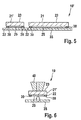
- the substrate arrangement 10 comprises a carrier 35.
- the carrier 35 can be, for example, a transfer element, in particular a transfer film.
- the substrate 20 is provided with the applied prefixing agent 30 and the applied Contacting material 25 is arranged to the carrier 35 such that the first side 22 of the substrate 20 is arranged facing the carrier 35. In other words, the first side 22 of the substrate 20 to the carrier 35.
- at least the prefixing agent 30 is adhesively bonded to the carrier 35. It is also possible that the contacting material 25 is also adhesively bonded to the carrier 35.
- the prefixing agent 30 and the carrier 35 acts such an adhesion force that the substrate assembly 10 is easy to transport, wherein the substrate 20 can not detach from the carrier 35 during transport.
- the adhesion force between the prefixing agent 30 and the carrier 35 is so small that the substrate 20 together with the prefixing agent 30 and the contacting material 25 can be detached from the carrier 35 if a component is to be connected to the substrate assembly 10.
- a substrate assembly 10 is shown, which is released by means of a nozzle 40 from the carrier 35.
- the detachment of the substrate 20 together with the Vorfixierstoff 30 and the bonding material 25 from the carrier 35 can be performed for example in the context of a pick and place process using the nozzle 40.
- FIGS. 7 to 9 show a method for connecting an electronic component 50 to a substrate assembly 10 according to a first embodiment of the invention.
- the substrate assembly 10 is first removed by means of the nozzle 40 from a carrier 35.
- the substrate arrangement 10 is positioned with the aid of the nozzle 40 on the electronic component 50 such that the first side 22 of the substrate 20 is arranged facing the electronic component 50.
- the nozzle 40 acts on the second side 23 of the substrate 20.
- the substrate assembly 10 is placed on the electronic component 50, wherein only the Vorfixierstoff 30 touches the component 50 or only the Vorfixierstoff 30 is connected to the component 50.
- the illustrated component 50 may be, for example, a silicon semiconductor. Between the contacting material 25 and the component 50 is formed a distance, this distance being formed due to the different thicknesses of the prefixing agent and the contacting means.
- nozzle 40 is already removed from the substrate arrangement 10. There is a heat application at a temperature of 100 to 150 ° C. As a result, the prefixing agent 30 is activated so that a prefixing of the substrate assembly 10 to the electronic component 50 takes place.
- the prefixing is preferably an adhesive bond between the substrate 20, in particular the first side 22 of the substrate 20, and the electronic component 50, in particular the side 52 of the electronic component 50 facing the substrate 20, wherein the adhesive bond is produced on the basis of the prefixing means 30 is.
- the pre-drying or the drying step, as this in Fig. 4 is shown is optional. It is possible for the prefixing agent 30 to be applied to the first side 22 of the substrate 20, after which a prefixing of an electronic component 50, 51 to the substrate arrangement 10 takes place immediately thereafter. The formation of a carrier 35 is not necessary in this case. In this case, the prefixing agent 30 is applied to the substrate 20 immediately prior to placement on an electronic component 50, 51 or directly prior to placement on an electronic component 50, 51.
- the actual connection of the substrate assembly 10 takes place with the electronic component 50.
- the bonding can be done by soldering or pressing or sintering.
- the substrate assembly 10 is sintered to the electronic component 50.
- the organic / polymeric components of the prefixing agent 30 volatilize as much as possible. In other words, the prefixing agent 30 is at least partially removed, in particular burned off and / or melted off, during bonding or after bonding.
- residues 31 of the prefixing agent 30 are formed on the first side 52 of the electronic component.
- FIGS. 10 to 12 A method for connecting electronic components 50 and 51 to a substrate arrangement 10 according to a further exemplary embodiment is shown.
- a substrate arrangement 10 comprising two substrate sections 21 and 21 'is equipped with a first electronic component 50 and a second electronic component 51. Both the substrate section 21 and the substrate section 21 'comprise a contacting material 25 and prefixing means 30 formed laterally of the respective contacting material 25.
- Both the first electronic component 50 and the second electronic component 51 are positioned with the aid of nozzles 40 and 40 'to the substrate arrangement 10 such that the first side 22 of the substrate 20 is arranged facing the first electronic component 50 and the second electronic component 51.
- the first electronic component 50 may be a silicon semiconductor.
- the second electronic component 51 has a coating 54 both on the first side 52 and on the second side 53.
- FIG. 11 there is a prefixing of the substrate assembly 10 with the first electronic component 50 and the second electronic component 51 by the on the first side 22 of the substrate 20 partially applied Vorfixierstoff 30.
- Vorfixierstoffs 30 apply in connection with the FIGS. 1 to 9 listed explanations.
- the substrate arrangement 10 is joined together with the first electronic component 50 and the second electronic component 52 exposed to heat, especially at temperatures of 100 to 150 ° C.
- the result is an adhesive bond between the first electronic component 50 and the substrate 20, in particular between the first electronic component 50 and the first side 22 of the substrate 20.
- the substrate assembly 10 is connected to the first electronic component 50 and the second electronic component 51.
- the prefixing agent 30 is at least partially removed, in particular burned off and / or melted off.
- this remaining residue 31 of the prefixing agent 30 is the inorganic fillers of the original prefixing agent 30.
- the electronic component 50 and the second electronic component 51 are in Fig. 12 completely connected to the substrate assembly 10.
- the substrate assembly 10 includes a substrate 20 having a first side 22 and a second side 23. On the first side 22 of the substrate 20 is the remainder 31 of an original prefixing agent 30.
Landscapes
- Electric Connection Of Electric Components To Printed Circuits (AREA)
- Compositions Of Macromolecular Compounds (AREA)
Priority Applications (1)
| Application Number | Priority Date | Filing Date | Title |
|---|---|---|---|
| EP17182111.9A EP3276652A3 (fr) | 2015-04-02 | 2016-03-23 | Procédé de fabrication d'un agencement de substrat avec un moyen de pré-fixation à colle, agencement de substrat correspondant, procédé de connexion d'un composant électronique avec un agencement de substrat utilisant un moyen de pré-fixation à colle formé sur le composant électronique et/ou l'agencement de substrat et composant électronique connecté avec un agencement de substrat |
Applications Claiming Priority (2)
| Application Number | Priority Date | Filing Date | Title |
|---|---|---|---|
| DE102015105127 | 2015-04-02 | ||
| DE102015107724.8A DE102015107724B4 (de) | 2015-04-02 | 2015-05-18 | Verfahren zum Herstellen einer Substratanordnung, Substratanordnung, Verfahren zum Verbinden eines Elektronikbauteils mit einer Substratanordnung und Elektronikbauteil |
Related Child Applications (1)
| Application Number | Title | Priority Date | Filing Date |
|---|---|---|---|
| EP17182111.9A Division EP3276652A3 (fr) | 2015-04-02 | 2016-03-23 | Procédé de fabrication d'un agencement de substrat avec un moyen de pré-fixation à colle, agencement de substrat correspondant, procédé de connexion d'un composant électronique avec un agencement de substrat utilisant un moyen de pré-fixation à colle formé sur le composant électronique et/ou l'agencement de substrat et composant électronique connecté avec un agencement de substrat |
Publications (2)
| Publication Number | Publication Date |
|---|---|
| EP3086361A2 true EP3086361A2 (fr) | 2016-10-26 |
| EP3086361A3 EP3086361A3 (fr) | 2017-01-25 |
Family
ID=55589738
Family Applications (2)
| Application Number | Title | Priority Date | Filing Date |
|---|---|---|---|
| EP17182111.9A Withdrawn EP3276652A3 (fr) | 2015-04-02 | 2016-03-23 | Procédé de fabrication d'un agencement de substrat avec un moyen de pré-fixation à colle, agencement de substrat correspondant, procédé de connexion d'un composant électronique avec un agencement de substrat utilisant un moyen de pré-fixation à colle formé sur le composant électronique et/ou l'agencement de substrat et composant électronique connecté avec un agencement de substrat |
| EP16161902.8A Withdrawn EP3086361A3 (fr) | 2015-04-02 | 2016-03-23 | Procede de fabrication d'un agencement de substrat avec un moyen de pre-fixation, agencement de substrat correspondant, procede de connexion d'un composant electronique avec un agencement de substrat utiilisant un moyen de pre-fixation forme sur le composant electronique et/ou l'agencement de substrat et composant electronique connecte avec un agencement de substrat |
Family Applications Before (1)
| Application Number | Title | Priority Date | Filing Date |
|---|---|---|---|
| EP17182111.9A Withdrawn EP3276652A3 (fr) | 2015-04-02 | 2016-03-23 | Procédé de fabrication d'un agencement de substrat avec un moyen de pré-fixation à colle, agencement de substrat correspondant, procédé de connexion d'un composant électronique avec un agencement de substrat utilisant un moyen de pré-fixation à colle formé sur le composant électronique et/ou l'agencement de substrat et composant électronique connecté avec un agencement de substrat |
Country Status (1)
| Country | Link |
|---|---|
| EP (2) | EP3276652A3 (fr) |
Cited By (3)
| Publication number | Priority date | Publication date | Assignee | Title |
|---|---|---|---|---|
| EP3611761A1 (fr) * | 2018-08-13 | 2020-02-19 | Heraeus Deutschland GmbH & Co KG | Procédé et substrat métallique destinés à contacter un semi-conducteur de puissance par un moyen de contact avec au moins une zone sans le moyen de contact comme structure réductrice de contraintes |
| EP3690936A1 (fr) * | 2019-01-29 | 2020-08-05 | Heraeus Deutschland GmbH & Co KG | Procédé de fabrication d'un système d'espacement avec un logement pour une puce, système d'espacement correspondant et son utilisation pour contacter une puce à un substrat par frittage |
| WO2023280444A1 (fr) * | 2021-07-09 | 2023-01-12 | Heraeus Deutschland GmbH & Co. KG | Composition utilisable comme fixatif provisoire |
Families Citing this family (1)
| Publication number | Priority date | Publication date | Assignee | Title |
|---|---|---|---|---|
| EP3644348A1 (fr) * | 2018-10-23 | 2020-04-29 | Heraeus Deutschland GmbH & Co. KG | Procédé de fabrication d'un substrat |
Family Cites Families (22)
| Publication number | Priority date | Publication date | Assignee | Title |
|---|---|---|---|---|
| JPS6369785A (ja) * | 1986-09-12 | 1988-03-29 | 株式会社日立製作所 | 炭化ケイ素焼結体用メタライズペ−スト及び半導体装置 |
| DK54988A (da) * | 1987-11-25 | 1989-05-26 | Du Pont | Materiale til binding af integrerede kredsloeb til uorganiske, dielektriske underlag |
| JP2932840B2 (ja) * | 1992-08-06 | 1999-08-09 | 日本電気株式会社 | 半導体素子のボンディング方法 |
| JPH06196513A (ja) * | 1992-12-22 | 1994-07-15 | Hitachi Chem Co Ltd | 接着剤および半導体装置 |
| JP3464826B2 (ja) * | 1994-07-21 | 2003-11-10 | 株式会社東芝 | 半導体装置 |
| US5906310A (en) * | 1994-11-10 | 1999-05-25 | Vlt Corporation | Packaging electrical circuits |
| JP3243988B2 (ja) * | 1995-12-27 | 2002-01-07 | 松下電器産業株式会社 | 半導体装置の製造方法 |
| JPH1154550A (ja) * | 1997-07-31 | 1999-02-26 | Nec Kansai Ltd | 半導体装置及びその製造方法 |
| WO2001057112A1 (fr) * | 2000-02-01 | 2001-08-09 | Nippon Steel Chemical Co., Ltd. | Resine polyimide adhesive et stratifie adhesif |
| JP2002111191A (ja) * | 2000-10-04 | 2002-04-12 | Hitachi Ltd | はんだ接合方法およびこれを用いた電子回路装置 |
| US6946740B2 (en) * | 2002-07-15 | 2005-09-20 | International Rectifier Corporation | High power MCM package |
| JP5282981B2 (ja) * | 2007-12-21 | 2013-09-04 | 株式会社村田製作所 | 素子搭載基板の製造方法 |
| DE102007063308A1 (de) * | 2007-12-28 | 2009-07-02 | Robert Bosch Gmbh | Diode |
| DE102010021764B4 (de) * | 2010-05-27 | 2014-09-25 | Semikron Elektronik Gmbh & Co. Kg | Verfahren zur Niedertemperatur Drucksinterverbindung zweier Verbindungspartner |
| JP5676155B2 (ja) * | 2010-06-23 | 2015-02-25 | 日立アロカメディカル株式会社 | 放射線検出器の製造方法、及び放射線検出器 |
| JP5807221B2 (ja) * | 2010-06-28 | 2015-11-10 | アユミ工業株式会社 | 接合構造体製造方法および加熱溶融処理方法ならびにこれらのシステム |
| JP5091296B2 (ja) * | 2010-10-18 | 2012-12-05 | 東京エレクトロン株式会社 | 接合装置 |
| JP6011074B2 (ja) * | 2012-01-20 | 2016-10-19 | 富士通株式会社 | 電子装置の製造方法及び電子装置の製造装置 |
| US20140224409A1 (en) * | 2013-02-11 | 2014-08-14 | International Rectifier Corporation | Sintering Utilizing Non-Mechanical Pressure |
| JP6542504B2 (ja) * | 2013-02-20 | 2019-07-10 | 日東電工株式会社 | フィルム状接着剤、フィルム状接着剤付きダイシングテープ、半導体装置の製造方法、及び半導体装置 |
| JP5664679B2 (ja) * | 2013-03-07 | 2015-02-04 | 三菱マテリアル株式会社 | パワーモジュール用基板の製造方法 |
| DE102013208387A1 (de) * | 2013-05-07 | 2014-11-13 | Robert Bosch Gmbh | Silber-Komposit-Sinterpasten für Niedertemperatur Sinterverbindungen |
-
2016
- 2016-03-23 EP EP17182111.9A patent/EP3276652A3/fr not_active Withdrawn
- 2016-03-23 EP EP16161902.8A patent/EP3086361A3/fr not_active Withdrawn
Non-Patent Citations (1)
| Title |
|---|
| None |
Cited By (3)
| Publication number | Priority date | Publication date | Assignee | Title |
|---|---|---|---|---|
| EP3611761A1 (fr) * | 2018-08-13 | 2020-02-19 | Heraeus Deutschland GmbH & Co KG | Procédé et substrat métallique destinés à contacter un semi-conducteur de puissance par un moyen de contact avec au moins une zone sans le moyen de contact comme structure réductrice de contraintes |
| EP3690936A1 (fr) * | 2019-01-29 | 2020-08-05 | Heraeus Deutschland GmbH & Co KG | Procédé de fabrication d'un système d'espacement avec un logement pour une puce, système d'espacement correspondant et son utilisation pour contacter une puce à un substrat par frittage |
| WO2023280444A1 (fr) * | 2021-07-09 | 2023-01-12 | Heraeus Deutschland GmbH & Co. KG | Composition utilisable comme fixatif provisoire |
Also Published As
| Publication number | Publication date |
|---|---|
| EP3086361A3 (fr) | 2017-01-25 |
| EP3276652A2 (fr) | 2018-01-31 |
| EP3276652A3 (fr) | 2018-04-25 |
Similar Documents
| Publication | Publication Date | Title |
|---|---|---|
| DE102015107724B4 (de) | Verfahren zum Herstellen einer Substratanordnung, Substratanordnung, Verfahren zum Verbinden eines Elektronikbauteils mit einer Substratanordnung und Elektronikbauteil | |
| DE102013216633B4 (de) | Vorgesinterte Halbleiterchip-Struktur und Verfahren zum Herstellen | |
| DE102004019567B3 (de) | Verfahren zur Befestigung von elektronischen Bauelementen auf einem Substrat | |
| EP3103138B1 (fr) | Procédé de montage d'un composant électrique en utilisant un capot | |
| DE1591186B1 (de) | Verfahren zum simultanen Herstellen von Zufuehrungs-verbindungen mittels Kontaktbruecken auf Festkoerperbauelementen mit Hilfe von abziehbildartigen Vorrichtungen | |
| DE19848834A1 (de) | Verfahren zum Montieren eines Flipchips und durch dieses Verfahren hergestellte Halbleiteranordnung | |
| EP3940758A2 (fr) | Procédé de connexion par frittage d'un agencement de substrat avec un composant électronique utilisant un moyen de pré-fixation sur une couche de matériau de frittage de contact, agencement de substrat correspondant et procédé de sa fabrication | |
| DE10250778B3 (de) | Elektronisches Bauteil mit einem Halbleiterchip und Verfahren zum Bestücken eines Schaltungsträgers beim Herstellen des elektronischen Bauteils | |
| EP3086361A2 (fr) | Procede de fabrication d'un agencement de substrat avec un moyen de pre-fixation, agencement de substrat correspondant, procede de connexion d'un composant electronique avec un agencement de substrat utiilisant un moyen de pre-fixation forme sur le composant electronique et/ou l'agencement de substrat et composant electronique connecte avec un agencement de substrat | |
| DE102009018541A1 (de) | Kontaktierungsmittel und Verfahren zur Kontaktierung elektrischer Bauteile | |
| WO2014086519A1 (fr) | Procédés destinés à relier au moins deux composants en mettant en œuvre un processus de frittage | |
| DE102014109766B3 (de) | Verfahren zum Herstellen eines Substratadapters, Substratadapter und Verfahren zum Kontaktieren eines Halbleiterelements | |
| DE102013102637B4 (de) | Metall-Keramik-Substrat sowie Verfahren zum Herstellen eines derartigen Metall-Keramik-Substrates und Anordnung von derartigen Metall-Keramik-Substraten | |
| DE102006033702B3 (de) | Herstellungsverfahren für eine elektronische Schaltung in einer Package-on-Package-Konfiguration und elektronisches Bauelement in einer solchen Konfiguration | |
| DE10303588B3 (de) | Verfahren zur vertikalen Montage von Halbleiterbauelementen | |
| DE102012110382A1 (de) | Substrat sowie Verfahren zum Herstellen eines Substrates | |
| DE10036976B4 (de) | Verfahren zum Verbinden und Verbindungsaufbau eines thermoplastischen Harzmaterials | |
| EP3297410A1 (fr) | Gabarit de brasage et procede de fabrication d'un systeme de circuits imprimes | |
| EP3762171B1 (fr) | Procédé de fabrication d'un ensemble sandwich | |
| DE102014220204A1 (de) | Verfahren zum Herstellen einer Lötverbindung und Bauteileverbund | |
| DE102019111437B4 (de) | Verfahren zur Herstellung eines elektronischen Zwischenprodukts und Verfahren zur Herstellung eines Elektronik-Bauteils | |
| WO2015091260A1 (fr) | Procédé de fixation d'un composant sur un substrat | |
| EP3675153A1 (fr) | Procédé de fabrication d'un adaptateur de substrat et adaptateur de substrat destiné au raccordement à un composant électronique | |
| DE102010041917B4 (de) | Schaltungsanordnung und Verfahren zu deren Herstellung | |
| DE10312109A1 (de) | Herstellung von Lotkontakten auf einem Wafer unter Verwendung einer strukturierten Lotfolie |
Legal Events
| Date | Code | Title | Description |
|---|---|---|---|
| PUAI | Public reference made under article 153(3) epc to a published international application that has entered the european phase |
Free format text: ORIGINAL CODE: 0009012 |
|
| AK | Designated contracting states |
Kind code of ref document: A2 Designated state(s): AL AT BE BG CH CY CZ DE DK EE ES FI FR GB GR HR HU IE IS IT LI LT LU LV MC MK MT NL NO PL PT RO RS SE SI SK SM TR |
|
| AX | Request for extension of the european patent |
Extension state: BA ME |
|
| PUAL | Search report despatched |
Free format text: ORIGINAL CODE: 0009013 |
|
| AK | Designated contracting states |
Kind code of ref document: A3 Designated state(s): AL AT BE BG CH CY CZ DE DK EE ES FI FR GB GR HR HU IE IS IT LI LT LU LV MC MK MT NL NO PL PT RO RS SE SI SK SM TR |
|
| AX | Request for extension of the european patent |
Extension state: BA ME |
|
| RIC1 | Information provided on ipc code assigned before grant |
Ipc: H01L 21/58 20060101AFI20161219BHEP Ipc: H01L 23/498 20060101ALI20161219BHEP Ipc: H01L 23/373 20060101ALI20161219BHEP Ipc: H05K 3/34 20060101ALI20161219BHEP Ipc: H01L 21/683 20060101ALI20161219BHEP Ipc: H01L 23/495 20060101ALI20161219BHEP Ipc: H01L 21/60 20060101ALI20161219BHEP Ipc: H05K 3/32 20060101ALI20161219BHEP |
|
| STAA | Information on the status of an ep patent application or granted ep patent |
Free format text: STATUS: THE APPLICATION IS DEEMED TO BE WITHDRAWN |
|
| 18D | Application deemed to be withdrawn |
Effective date: 20170726 |