EP3087660B1 - Harmonischer harvester für verbesserte rf-zu-dc-gleichrichtung - Google Patents
Harmonischer harvester für verbesserte rf-zu-dc-gleichrichtung Download PDFInfo
- Publication number
- EP3087660B1 EP3087660B1 EP14869326.0A EP14869326A EP3087660B1 EP 3087660 B1 EP3087660 B1 EP 3087660B1 EP 14869326 A EP14869326 A EP 14869326A EP 3087660 B1 EP3087660 B1 EP 3087660B1
- Authority
- EP
- European Patent Office
- Prior art keywords
- circuit
- output
- signals
- input
- blocking
- Prior art date
- Legal status (The legal status is an assumption and is not a legal conclusion. Google has not performed a legal analysis and makes no representation as to the accuracy of the status listed.)
- Not-in-force
Links
Images


Classifications
-
- H—ELECTRICITY
- H02—GENERATION; CONVERSION OR DISTRIBUTION OF ELECTRIC POWER
- H02J—ELECTRIC POWER NETWORKS; CIRCUIT ARRANGEMENTS OR SYSTEMS FOR SUPPLYING OR DISTRIBUTING ELECTRIC POWER; SYSTEMS FOR STORING ELECTRIC ENERGY
- H02J4/00—Circuit arrangements for mains or distribution networks not specified as AC or DC; Circuit arrangements for mains or distribution networks combining AC and DC sections or sub-networks
- H02J4/20—Networks integrating separated AC and DC power sections
- H02J4/25—Networks integrating separated AC and DC power sections for transfer of electric power between AC and DC networks, e.g. for supplying the DC section within a load from an AC mains system
-
- H—ELECTRICITY
- H02—GENERATION; CONVERSION OR DISTRIBUTION OF ELECTRIC POWER
- H02M—APPARATUS FOR CONVERSION BETWEEN AC AND AC, BETWEEN AC AND DC, OR BETWEEN DC AND DC, AND FOR USE WITH MAINS OR SIMILAR POWER SUPPLY SYSTEMS; CONVERSION OF DC OR AC INPUT POWER INTO SURGE OUTPUT POWER; CONTROL OR REGULATION THEREOF
- H02M1/00—Details of apparatus for conversion
- H02M1/0048—Circuits or arrangements for reducing losses
-
- H—ELECTRICITY
- H02—GENERATION; CONVERSION OR DISTRIBUTION OF ELECTRIC POWER
- H02M—APPARATUS FOR CONVERSION BETWEEN AC AND AC, BETWEEN AC AND DC, OR BETWEEN DC AND DC, AND FOR USE WITH MAINS OR SIMILAR POWER SUPPLY SYSTEMS; CONVERSION OF DC OR AC INPUT POWER INTO SURGE OUTPUT POWER; CONTROL OR REGULATION THEREOF
- H02M7/00—Conversion of AC power input into DC power output; Conversion of DC power input into AC power output
- H02M7/02—Conversion of AC power input into DC power output without possibility of reversal
- H02M7/04—Conversion of AC power input into DC power output without possibility of reversal by static converters
- H02M7/06—Conversion of AC power input into DC power output without possibility of reversal by static converters using discharge tubes without control electrode or semiconductor devices without control electrode
-
- H—ELECTRICITY
- H02—GENERATION; CONVERSION OR DISTRIBUTION OF ELECTRIC POWER
- H02M—APPARATUS FOR CONVERSION BETWEEN AC AND AC, BETWEEN AC AND DC, OR BETWEEN DC AND DC, AND FOR USE WITH MAINS OR SIMILAR POWER SUPPLY SYSTEMS; CONVERSION OF DC OR AC INPUT POWER INTO SURGE OUTPUT POWER; CONTROL OR REGULATION THEREOF
- H02M7/00—Conversion of AC power input into DC power output; Conversion of DC power input into AC power output
- H02M7/02—Conversion of AC power input into DC power output without possibility of reversal
- H02M7/04—Conversion of AC power input into DC power output without possibility of reversal by static converters
- H02M7/06—Conversion of AC power input into DC power output without possibility of reversal by static converters using discharge tubes without control electrode or semiconductor devices without control electrode
- H02M7/066—Conversion of AC power input into DC power output without possibility of reversal by static converters using discharge tubes without control electrode or semiconductor devices without control electrode particular circuits having a special characteristic
-
- H—ELECTRICITY
- H02—GENERATION; CONVERSION OR DISTRIBUTION OF ELECTRIC POWER
- H02M—APPARATUS FOR CONVERSION BETWEEN AC AND AC, BETWEEN AC AND DC, OR BETWEEN DC AND DC, AND FOR USE WITH MAINS OR SIMILAR POWER SUPPLY SYSTEMS; CONVERSION OF DC OR AC INPUT POWER INTO SURGE OUTPUT POWER; CONTROL OR REGULATION THEREOF
- H02M1/00—Details of apparatus for conversion
- H02M1/12—Arrangements for reducing harmonics from AC input or output
-
- H—ELECTRICITY
- H02—GENERATION; CONVERSION OR DISTRIBUTION OF ELECTRIC POWER
- H02M—APPARATUS FOR CONVERSION BETWEEN AC AND AC, BETWEEN AC AND DC, OR BETWEEN DC AND DC, AND FOR USE WITH MAINS OR SIMILAR POWER SUPPLY SYSTEMS; CONVERSION OF DC OR AC INPUT POWER INTO SURGE OUTPUT POWER; CONTROL OR REGULATION THEREOF
- H02M7/00—Conversion of AC power input into DC power output; Conversion of DC power input into AC power output
- H02M7/02—Conversion of AC power input into DC power output without possibility of reversal
- H02M7/04—Conversion of AC power input into DC power output without possibility of reversal by static converters
- H02M7/05—Capacitor coupled rectifiers
-
- Y—GENERAL TAGGING OF NEW TECHNOLOGICAL DEVELOPMENTS; GENERAL TAGGING OF CROSS-SECTIONAL TECHNOLOGIES SPANNING OVER SEVERAL SECTIONS OF THE IPC; TECHNICAL SUBJECTS COVERED BY FORMER USPC CROSS-REFERENCE ART COLLECTIONS [XRACs] AND DIGESTS
- Y02—TECHNOLOGIES OR APPLICATIONS FOR MITIGATION OR ADAPTATION AGAINST CLIMATE CHANGE
- Y02B—CLIMATE CHANGE MITIGATION TECHNOLOGIES RELATED TO BUILDINGS, e.g. HOUSING, HOUSE APPLIANCES OR RELATED END-USER APPLICATIONS
- Y02B70/00—Technologies for an efficient end-user side electric power management and consumption
- Y02B70/10—Technologies improving the efficiency by using switched-mode power supplies [SMPS], i.e. efficient power electronics conversion e.g. power factor correction or reduction of losses in power supplies or efficient standby modes
Definitions
- Conventional rectifying circuit design converts alternating-current (AC) signals into a direct-current (DC) signal.
- DC direct-current
- Low-barrier Schottky diodes are often used in low AC power cases such as ambient RF signals.
- the AC-to-DC conversion bandwidth and efficiency are related to AC power level, diode characteristics, and load impedance. The diode characteristics also depend on frequency, input power level, and output current.
- Exemplary embodiments of the present invention relate generally to a novel harmonic harvesting circuit design for harvesting un-rectified AC power (contained in the fundamental and harmonic frequencies) at the output of conventional rectifying circuits. It is appreciated that the present invention can also be used with other types of conventional AC-to-DC converter circuits that have similar problems as the conventional rectifying circuits.
- this invention can improve rectifying efficiency as well as extend the upper frequency limit of conventional rectifying circuits, and thus enabling efficient energy harvesting from radio frequency (RF) signals at higher frequencies used for GSM (Global System for Mobile Communications) or Wi-Fi from 700 MHz to 2500 MHz.
- RF radio frequency
- One of the most important components in RF energy harvesting is a rectifier which converts RF signals into DC power.
- Low-barrier Schottky diodes are often used as switches in low-power, high-frequency rectifier circuitry due to their low turn-on voltage, small resistance, and small junction capacitance.
- typical conversion efficiency of ambient RF harvesters are less than 60% due to ohmic loss in diode resistance and un-rectified energy in the harmonics produced by the diode's non-linear I-V property and the rectifying process.
- Un-rectified signals/energy are AC signals/energy that are not converted into a DC signal/energy by the rectifying circuit.
- Rectifying efficiency higher than 50% is very difficult to achieve at low RF input power level as in the case of most ambient RF signals, and can only be achieved under very optimal conditions of impedance matching, input power level, frequency, and load impedance.
- the output harmonics has been shown in the literature to contain as much as 20% of energy which is wasted in conventional rectifier designs.
- the novel circuitry of the present invention can also improve the rectifying efficiency at the upper frequency limit of the rectifying diode where some portion of the input RF signal bypass the diode through its junction capacitance. This produces un-rectified RF signals at the fundamental frequency at the output of conventional rectifiers. Such RF signals are shorted to the ground by the large DC hold capacitor, and thus being wasted.
- a harvester circuit of the present invention connects between the output and input of a conventional rectifier circuit, thus forming a feedback loop circuitry. Additional embodiments of variations of harvester circuit topologies are comprised of different arrangement of rectifying diodes, filters, and impedance matching circuits.
- NAOKI SHINOHARA "Rectennas for microwave power transmission", IEICE ELECTRONICS EXPRESS, vol. 10, no. 21, 10 November 2013 relates to a rectifying antenna used in microwave power transmission (MPT) that converts a microwave signal to a DC signal by using a rectifying diode.
- MPT microwave power transmission
- Exemplary embodiments of the present invention are directed to improvements in RF to DC conversion efficiency, defined as the ratio of the final DC output power to the input RF power. All simulated results were obtained using the commercial Advanced Design System Circuit Design Cookbook. In the following description the term "embodiment” may have been used for subject-matter that is not part of the invention as defined by the appended claims.
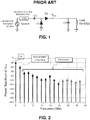
- FIG. 1 an exemplary embodiment of a standard Greinacher Voltage Doubler circuit commonly used to convert RF signals into DC power is shown.
- a single 2.45 GHz tone RF source at -10 dBm power level enters the circuit from the left. It is followed by an impedance matching circuit comprised of a single-stub tuner for minimizing reflection back into the source.
- the capacitor C1 is for blocking the DC signal from going to the RF source while allowing the RF signal from the source to pass through.
- two rectifying diodes D1 and D2 that are the SMS7630 low-barrier Schottky diodes.
- the rectified output DC signal level is smoothed by the charge holding capacitor C2.
- the output is connected to a 1K resistor at the right hand side.
- FIG 3 shows an exemplary embodiment of harmonic harvester 10 block added to the output of the conventional rectifier 12 shown in Figure 1 .
- the harmonic harvester circuit block in this exemplary embodiment is comprised of a DC blocking capacitor C2 14 , followed by an impedance match network circuit 16 (IMN2), a rectifying diode D3 18 , and a RF blocking inductor L1 20 for preventing fundamental and harmonic signals from getting shorted to the ground through C3.
- IPN2 impedance match network circuit
- D3 rectifying diode
- L1 20 RF blocking inductor
- the un-rectified RF energy present at the fundamental and harmonic frequencies at the output of D2 is stopped by the RF blocking inductor L1 and redirected to the harmonic harvester circuit that is comprised of the DC blocking capacitor C2, an impedance matching circuit IMN2 (which is preferably different from IMN1), and rectifying diode D3 (which in one embodiment is the same as D1 and D2, but it does not have to be the same).
- IMN2 which is preferably different from IMN1
- D3 rectifying diode D3
- additional components could be added to provide a more sophisticated frequency control.
- a simple high-pass filter may be used; instead of a single inductor L, a simple low-pass filter may be used.
- These electrical circuit elements can also be replaced with more complicated L/C circuitry to achieve a more sophisticated filtering.
- the frequency of the input signal is increased from 2.45 GHz to 5.8 GHz to demonstrate reduced conversion efficiency due to more RF energy leaking through the junction capacitance of D1 and D2. Comparing the output DC power level in the Figure 5 output power spectrum to that obtained in Figure 2 at 2.45 GHz shows significant DC power reduction. The conversion efficiency in this case is 16%.
- the frequency of the input signal is increased from 2.45 GHz to 5.8 GHz.
- the output power spectrum in Figure 6 shows that the DC power is increased compared to that in Figure 5 .
- the resultant conversion efficiency increases from 16% to 22%.
- Figure 7 shows an exemplary embodiment of the present invention of connecting multiple harmonic harvesters 22 in a cascade (series) fashion for harvesting more power into DC - especially in high-leakage situations as the output of each harmonic harvester could still have non-DC component. It is important to keep the number of the harmonic harvesters to a minimal since additional diodes in each harmonic harvester circuit also add more ohmic loss, and thus lowering conversion efficiency.
- Figure 8 shows an exemplary embodiment of connecting a single, or multiple harmonic harvesters, in a loop-back 24 configuration.
- This configuration is equivalent to the multiple harmonic harvester embodiment without using multiple circuits, thus saving size and cost compared to the series configuration shown in Figure 7 .
- the dotted line around the harmonic harvester portion of the circuit in Figure 8 is a general representation that the harvester circuits of the present invention (e.g., harvester circuits of Figures 3 , 7 ) can be used as a feedback loop in Figure 8 (for example, use of the harvester circuits of Figures 3 and 7 as a feedback loop requires taking the loop back to the input of the rectifier D2).
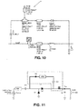
- Figure 11 illustrates one example embodiment of the feedback loop circuit of Figure 8 .
- Figure 9(a) shows an exemplary circuit implementing the single harmonic harvester design (based on the Figure 3 design).
- Figure 9(b) shows the fabricated circuit board and the measured conversion efficiency (dashed line) as a function of input power in comparison with the measured conversion efficiency (solid line) without the harmonic harvester. In this case, the harmonic harvest increases the conversion efficiency by 5% to 18% for input power above -5 dBm.
- Figure 10 shows an example of an ADS circuit model implementation of a harmonic harvester circuit.
- the impedance matching network IMN portion 26 of the circuit is comprised of a section of transmission line TL69 and tee junction T9, and a shorted stub TL68.
- the ADS will search automatically for the best lengths of TL69 and TL68 that produce maximum DC output.
Landscapes
- Engineering & Computer Science (AREA)
- Power Engineering (AREA)
- Rectifiers (AREA)
Claims (13)
- Elektrische Schaltung (10) zum Auffangen von nicht gleichgerichteten oder sogenannten nicht umgewandelten HF-Signalen bei der Grundfrequenz an einem Ausgang eines AC-Gleichstrom-(AC/DC)-Wandlerschaltkreises (12), die Folgendes umfasst:einen DC-Sperrstromkreis (14), der so konfiguriert ist, dass er in Verbindung mit dem Ausgang des AC/DC-Wandlerschaltkreises (12) steht, der dafür ausgelegt ist, DC-Signale und die nicht umgewandelten AC-Signale zu generieren, wobei der DC-Sperrstromkreis (14) einen Eingang und einen Ausgang aufweist, die so angelegt sind, dass sie die nicht umgewandelten AC-Signale passieren lassen und die DC-Signale blockieren;einen Impedanzanpassungsstromkreis (16) mit einem Eingang und einem Ausgang, der so angelegt ist, dass er die nicht umgewandelten AC-Signale empfängt, wobei der Eingang des Impedanzanpassungsstromkreises (16) in Verbindung mit dem Ausgang des DC-Sperrstromkreises (20) steht;einen Gleichrichter (18) mit einem Eingang und einem Ausgang, der so angelegt ist, dass er die nicht umgewandelten AC-Signale gleichrichtet, wobei der Eingang des Gleichrichters (18) in Verbindung mit dem Ausgang des Impedanzanpassungsstromkreises (16) steht; undeinen AC-Sperrstromkreis (20) mit einem Eingang und einem Ausgang, der so angelegt ist, dass er die DC-Signale passieren lässt und die nicht umgewandelten AC-Signale blockiert, wobei der Eingang des AC-Sperrstromkreises (20) in Verbindung sowohl mit dem Ausgang des AC/DC-Wandlerschaltkreises (12) als auch dem Eingang des DC-Sperrstromkreises (14) steht.
- Elektrische Schaltung (10) nach Anspruch 1, wobei der Ausgang des AC-Sperrstromkreises (20) in Verbindung mit dem Ausgang des Gleichrichters (18) steht und wobei der Ausgang des AC-Sperrstromkreises (20) und der Ausgang des Gleichrichters (18) den Ausgang der elektrischen Schaltung (10) bilden.
- Elektrische Schaltung (10) nach Anspruch 1, wobei die nicht umgewandelten AC-Signale eines der Oberwellensignale eines entsprechenden AC-Signals sind, die an einem Eingang des AC/DC-Wandlerschaltkreises (12) empfangen werden, deren Frequenzen Vielfache einer Grundfrequenz des entsprechenden AC-Signals sind und ein Hochfrequenzsignal (HF) enthalten, das zum Ausgang des AC/DC-Wandlerschaltkreises (12) durchgedrungen ist.
- Elektrische Schaltung (10) nach Anspruch 1, wobei der DC-Sperrstromkreis (14) ein Kondensator oder ein Hochpassfilter ist.
- Elektrische Schaltung (10) nach Anspruch 1, wobei der AC-Sperrstromkreis (20) ein Induktor oder ein Tiefpassfilter ist.
- Elektrische Schaltung (10) nach Anspruch 1, wobei der AC-Sperrstromkreis (20) so angelegt ist, dass er verhindert, dass Grund- und Oberwellensignale eines entsprechenden, am Eingang des AC/DC-Wandlerschaltkreises (12) empfangenen AC-Signals mit der Erde kurzgeschlossen werden.
- Schaltung (10), die eine erste und zweite elektrische Schaltung (22) umfasst, die in Reihe geschaltet sind und entsprechend einer elektrischen Schaltung (10) nach Anspruch 1 entsprechen, wobei die erste und zweite elektrische Schaltung (22) so angelegt sind, dass sie die nicht umgewandelten Wechselstrom-(AC)-Signale am Ausgang des AC/DC-Wandlerschaltkreises (12) auffangen.
- Elektrische Schaltung (10) nach Anspruch 1, wobei der Ausgang des Gleichrichters (18) in Verbindung mit einem Eingang des AC/DC-Wandlerschaltkreises (12) steht, um eine Rückkopplungsschleife auszubilden.
- Elektrische Schaltung (10) nach Anspruch 1, wobei der Ausgang des Gleichrichters (18) in Verbindung mit einem Eingang des AC/DC-Wandlerschaltkreises (12) steht, um eine Rückkopplungsschleife auszubilden.
- Elektrische Schaltung (10) nach Anspruch 9, wobei der Ausgang des AC-Sperrstromkreises (20) in Verbindung mit einer Last steht.
- Elektrische Schaltung (10) nach Anspruch 9, wobei der AC-Sperrstromkreis (20) so angelegt ist, dass er verhindert, dass Grund- und Oberwellensignale eines entsprechenden, am Eingang des AC/DC-Wandlerschaltkreises (12) empfangenen AC-Signals mit der Erde kurzgeschlossen werden.
- Elektrische Schaltung (10) nach Anspruch 9, wobei der DC-Sperrstromkreis (14) ein Kondensator oder ein Hochpassfilter ist.
- Elektrische Schaltung (10) nach Anspruch 9, wobei der AC-Sperrstromkreis (20) ein Induktor oder ein Tiefpassfilter ist.
Applications Claiming Priority (2)
| Application Number | Priority Date | Filing Date | Title |
|---|---|---|---|
| US201361915237P | 2013-12-12 | 2013-12-12 | |
| PCT/US2014/070087 WO2015089437A1 (en) | 2013-12-12 | 2014-12-12 | Harmonic harvester for improved rf-to-dc rectifying efficiency |
Publications (3)
| Publication Number | Publication Date |
|---|---|
| EP3087660A1 EP3087660A1 (de) | 2016-11-02 |
| EP3087660A4 EP3087660A4 (de) | 2017-08-09 |
| EP3087660B1 true EP3087660B1 (de) | 2018-09-19 |
Family
ID=53371881
Family Applications (1)
| Application Number | Title | Priority Date | Filing Date |
|---|---|---|---|
| EP14869326.0A Not-in-force EP3087660B1 (de) | 2013-12-12 | 2014-12-12 | Harmonischer harvester für verbesserte rf-zu-dc-gleichrichtung |
Country Status (6)
| Country | Link |
|---|---|
| US (2) | US10063063B2 (de) |
| EP (1) | EP3087660B1 (de) |
| JP (1) | JP2016540485A (de) |
| KR (1) | KR20160105421A (de) |
| CN (1) | CN106464149B (de) |
| WO (1) | WO2015089437A1 (de) |
Families Citing this family (12)
| Publication number | Priority date | Publication date | Assignee | Title |
|---|---|---|---|---|
| US20200251912A1 (en) * | 2013-12-12 | 2020-08-06 | Nikola Labs | Systems and methods for machine condition monitoring powered by efficient harmonic harvester |
| EP3087660B1 (de) * | 2013-12-12 | 2018-09-19 | The Ohio State Innovation Foundation | Harmonischer harvester für verbesserte rf-zu-dc-gleichrichtung |
| US9768708B2 (en) * | 2015-09-08 | 2017-09-19 | The Regents Of The University Of Michigan | Wide dynamic range rectifier circuits |
| GB2538576B (en) | 2015-09-14 | 2017-06-14 | Drayson Tech (Europe) Ltd | RF-to-DC Converter |
| GB2538575B (en) * | 2015-09-14 | 2017-06-14 | Drayson Tech (Europe) Ltd | RF-to-DC Converter |
| US9966656B1 (en) | 2016-11-08 | 2018-05-08 | Aeternum LLC | Broadband rectenna |
| GB2558647B (en) * | 2017-01-13 | 2019-01-02 | Drayson Tech Europe Ltd | RF to DC converter |
| JP6304520B1 (ja) * | 2017-07-27 | 2018-04-04 | 株式会社レーザーシステム | 半導体装置 |
| US11133576B2 (en) | 2017-08-28 | 2021-09-28 | Aeternum, LLC | Rectenna |
| KR102096203B1 (ko) * | 2019-04-17 | 2020-04-01 | 주식회사 지오플랜코리아 | 무선 전력 전송 방식을 이용한 방사형 전력 공급 시스템 |
| KR102790323B1 (ko) | 2019-08-23 | 2025-04-07 | 주식회사 시솔지주 | 지문 인식 카드 |
| FR3106707B1 (fr) * | 2020-01-24 | 2023-09-29 | Vitesco Technologies | Dispositif de traitement d’un signal contrôle pilote |
Family Cites Families (20)
| Publication number | Priority date | Publication date | Assignee | Title |
|---|---|---|---|---|
| JPH079590Y2 (ja) | 1990-02-13 | 1995-03-06 | 株式会社トーキン | 整流平滑回路 |
| JP3063513B2 (ja) | 1994-02-10 | 2000-07-12 | 松下電器産業株式会社 | マイクロ波検波給電回路 |
| JPH0822513A (ja) * | 1994-07-08 | 1996-01-23 | Takasago Seisakusho:Kk | カード装置 |
| JP3761293B2 (ja) * | 1997-08-06 | 2006-03-29 | Necエンジニアリング株式会社 | レクテナ装置 |
| JP2002233083A (ja) | 2001-01-30 | 2002-08-16 | Nissin Electric Co Ltd | 高調波エネルギ再利用装置およびシステム |
| WO2005039028A2 (en) | 2003-10-17 | 2005-04-28 | Firefly Power Technologies, Inc. | Method and apparatus for a wireless power supply |
| EP1959825B1 (de) * | 2005-10-24 | 2020-04-22 | Powercast Corporation | Verfahren und vorrichtung für einen hocheffizienten gleichrichter für verschiedene lasten |
| US20090152954A1 (en) * | 2007-07-17 | 2009-06-18 | Triet Tu Le | RF energy harvesting circuit |
| JP4985208B2 (ja) | 2007-08-10 | 2012-07-25 | 株式会社デンソー | 倍電圧整流回路 |
| US7646214B2 (en) | 2007-11-28 | 2010-01-12 | Intel Corporation | Power harvesting signal line termination |
| US8432070B2 (en) * | 2008-08-25 | 2013-04-30 | Qualcomm Incorporated | Passive receivers for wireless power transmission |
| US8115571B2 (en) * | 2008-11-28 | 2012-02-14 | Schaffner Emv Ag | Harmonic filter |
| KR20110133856A (ko) * | 2010-06-07 | 2011-12-14 | 삼성전기주식회사 | 무선전력전송 시스템의 정류 회로 |
| WO2012129096A1 (en) | 2011-03-18 | 2012-09-27 | George Albert Mazzoli | Method and system for applying power harmonics to loads |
| JP2012222394A (ja) | 2011-04-04 | 2012-11-12 | Wave Technology Inc | 電力増幅器 |
| US20120313728A1 (en) * | 2011-06-10 | 2012-12-13 | Cairo Jr John Louis | Apparatus for Capturing Electric Distribution System Harmonics for Powering Loads |
| WO2013031787A1 (ja) | 2011-08-26 | 2013-03-07 | 日本電気株式会社 | 整流回路及び整流方法 |
| US20130077360A1 (en) * | 2011-09-26 | 2013-03-28 | Qualcomm Incorporated | Systems, methods, and apparatus for rectifier filtering for input waveform shaping |
| GB2510393A (en) * | 2013-02-01 | 2014-08-06 | Nujira Ltd | An envelope-tracking amplifier with a linear amplifier having an output offset current for improved efficiency |
| EP3087660B1 (de) * | 2013-12-12 | 2018-09-19 | The Ohio State Innovation Foundation | Harmonischer harvester für verbesserte rf-zu-dc-gleichrichtung |
-
2014
- 2014-12-12 EP EP14869326.0A patent/EP3087660B1/de not_active Not-in-force
- 2014-12-12 CN CN201480075533.4A patent/CN106464149B/zh not_active Expired - Fee Related
- 2014-12-12 JP JP2016539193A patent/JP2016540485A/ja active Pending
- 2014-12-12 US US15/103,557 patent/US10063063B2/en active Active
- 2014-12-12 WO PCT/US2014/070087 patent/WO2015089437A1/en not_active Ceased
- 2014-12-12 KR KR1020167018755A patent/KR20160105421A/ko not_active Withdrawn
-
2018
- 2018-06-26 US US16/019,071 patent/US10637255B2/en active Active
Non-Patent Citations (1)
| Title |
|---|
| None * |
Also Published As
| Publication number | Publication date |
|---|---|
| CN106464149B (zh) | 2019-04-23 |
| US20160315478A1 (en) | 2016-10-27 |
| JP2016540485A (ja) | 2016-12-22 |
| US20180309303A1 (en) | 2018-10-25 |
| WO2015089437A1 (en) | 2015-06-18 |
| KR20160105421A (ko) | 2016-09-06 |
| US10637255B2 (en) | 2020-04-28 |
| US10063063B2 (en) | 2018-08-28 |
| EP3087660A4 (de) | 2017-08-09 |
| CN106464149A (zh) | 2017-02-22 |
| EP3087660A1 (de) | 2016-11-02 |
Similar Documents
| Publication | Publication Date | Title |
|---|---|---|
| EP3087660B1 (de) | Harmonischer harvester für verbesserte rf-zu-dc-gleichrichtung | |
| Abdelhalem et al. | An RF–DC converter with wide-dynamic-range input matching for power recovery applications | |
| Valenta et al. | Rectenna performance under power-optimized waveform excitation | |
| US10063103B2 (en) | Contactless power transmission device and power transmission method thereof | |
| KR20170119325A (ko) | 무선 디바이스로부터 에너지를 자가 수확할 수 있는 시스템 및 이를 사용하는 방법 | |
| CN108347101A (zh) | 多模式无线电源接收电路及其控制方法 | |
| CN111262045B (zh) | 一种宽动态输入功率范围的紧凑型整流天线 | |
| Ouda et al. | Optimal operation of multitone waveforms in low RF-power receivers | |
| Mabrouki et al. | High efficiency low power rectifier design using zero bias schottky diodes | |
| Halimi et al. | Design of a 2.45 GHz operated Rectifier with 81.5% PCE at 13 dBm Input Power for RFEH/WPT Applications | |
| Mouapi et al. | Performances comparison of Shottky voltage doubler rectifier to support RF energy harvesting | |
| US20110298296A1 (en) | Rectifier circuit of wireless power transmission system | |
| US20160308398A1 (en) | Rectifying circuit for high-frequency power supply | |
| Rajabi et al. | Impact of multisine excitation design on rectifier performance | |
| JP6385171B2 (ja) | 整流器 | |
| Sakaki et al. | Modulated scheme and input power impact on rectifier RF-DC efficiency for WiCoPT system | |
| US9979315B2 (en) | Rectifying circuit for high-frequency power supply | |
| Wang et al. | Novel triband RF rectifier design for wireless energy harvesting | |
| Yao et al. | Optimal operation of RF energy rectifiers by adaptive number of frequency selection using multisine excitation | |
| Abdallah et al. | Wide power range RF energy harvesting circuit | |
| Wang et al. | Design of a broadband microwave rectifier from 40 MHz to 4740 MHz using high impedance inductor | |
| Hamzi et al. | Analysis of series and shunt rectifier circuits topologies | |
| Gupta et al. | High efficiency low power series diode rectifier design | |
| Wu et al. | A high efficiency rectifier for ambient RF energy harvesting at 940 MHz | |
| Shinohara et al. | Effects of output filter to RF-DC conversion efficiency in a rectenna |
Legal Events
| Date | Code | Title | Description |
|---|---|---|---|
| PUAI | Public reference made under article 153(3) epc to a published international application that has entered the european phase |
Free format text: ORIGINAL CODE: 0009012 |
|
| 17P | Request for examination filed |
Effective date: 20160711 |
|
| AK | Designated contracting states |
Kind code of ref document: A1 Designated state(s): AL AT BE BG CH CY CZ DE DK EE ES FI FR GB GR HR HU IE IS IT LI LT LU LV MC MK MT NL NO PL PT RO RS SE SI SK SM TR |
|
| AX | Request for extension of the european patent |
Extension state: BA ME |
|
| DAX | Request for extension of the european patent (deleted) | ||
| A4 | Supplementary search report drawn up and despatched |
Effective date: 20170707 |
|
| RIC1 | Information provided on ipc code assigned before grant |
Ipc: H02M 1/00 20070101ALN20170704BHEP Ipc: H02M 1/12 20060101ALN20170704BHEP Ipc: H02M 7/06 20060101AFI20170704BHEP |
|
| REG | Reference to a national code |
Ref country code: DE Ref legal event code: R079 Ref document number: 602014032790 Country of ref document: DE Free format text: PREVIOUS MAIN CLASS: H02J0050000000 Ipc: H02M0007060000 |
|
| RIC1 | Information provided on ipc code assigned before grant |
Ipc: H02M 1/12 20060101ALN20180227BHEP Ipc: H02M 7/06 20060101AFI20180227BHEP Ipc: H02M 1/00 20060101ALN20180227BHEP |
|
| RIC1 | Information provided on ipc code assigned before grant |
Ipc: H02M 1/00 20060101ALN20180302BHEP Ipc: H02M 1/12 20060101ALN20180302BHEP Ipc: H02M 7/06 20060101AFI20180302BHEP |
|
| GRAP | Despatch of communication of intention to grant a patent |
Free format text: ORIGINAL CODE: EPIDOSNIGR1 |
|
| RIC1 | Information provided on ipc code assigned before grant |
Ipc: H02M 1/00 20060101ALN20180319BHEP Ipc: H02M 7/06 20060101AFI20180319BHEP Ipc: H02M 1/12 20060101ALN20180319BHEP |
|
| RIC1 | Information provided on ipc code assigned before grant |
Ipc: H02M 1/12 20060101ALN20180327BHEP Ipc: H02M 7/06 20060101AFI20180327BHEP Ipc: H02M 1/00 20060101ALN20180327BHEP |
|
| INTG | Intention to grant announced |
Effective date: 20180416 |
|
| GRAS | Grant fee paid |
Free format text: ORIGINAL CODE: EPIDOSNIGR3 |
|
| GRAA | (expected) grant |
Free format text: ORIGINAL CODE: 0009210 |
|
| AK | Designated contracting states |
Kind code of ref document: B1 Designated state(s): AL AT BE BG CH CY CZ DE DK EE ES FI FR GB GR HR HU IE IS IT LI LT LU LV MC MK MT NL NO PL PT RO RS SE SI SK SM TR |
|
| REG | Reference to a national code |
Ref country code: GB Ref legal event code: FG4D |
|
| REG | Reference to a national code |
Ref country code: CH Ref legal event code: EP |
|
| REG | Reference to a national code |
Ref country code: AT Ref legal event code: REF Ref document number: 1044417 Country of ref document: AT Kind code of ref document: T Effective date: 20181015 |
|
| REG | Reference to a national code |
Ref country code: IE Ref legal event code: FG4D |
|
| REG | Reference to a national code |
Ref country code: DE Ref legal event code: R096 Ref document number: 602014032790 Country of ref document: DE |
|
| REG | Reference to a national code |
Ref country code: NL Ref legal event code: MP Effective date: 20180919 |
|
| PG25 | Lapsed in a contracting state [announced via postgrant information from national office to epo] |
Ref country code: SE Free format text: LAPSE BECAUSE OF FAILURE TO SUBMIT A TRANSLATION OF THE DESCRIPTION OR TO PAY THE FEE WITHIN THE PRESCRIBED TIME-LIMIT Effective date: 20180919 Ref country code: BG Free format text: LAPSE BECAUSE OF FAILURE TO SUBMIT A TRANSLATION OF THE DESCRIPTION OR TO PAY THE FEE WITHIN THE PRESCRIBED TIME-LIMIT Effective date: 20181219 Ref country code: RS Free format text: LAPSE BECAUSE OF FAILURE TO SUBMIT A TRANSLATION OF THE DESCRIPTION OR TO PAY THE FEE WITHIN THE PRESCRIBED TIME-LIMIT Effective date: 20180919 Ref country code: NO Free format text: LAPSE BECAUSE OF FAILURE TO SUBMIT A TRANSLATION OF THE DESCRIPTION OR TO PAY THE FEE WITHIN THE PRESCRIBED TIME-LIMIT Effective date: 20181219 Ref country code: FI Free format text: LAPSE BECAUSE OF FAILURE TO SUBMIT A TRANSLATION OF THE DESCRIPTION OR TO PAY THE FEE WITHIN THE PRESCRIBED TIME-LIMIT Effective date: 20180919 Ref country code: GR Free format text: LAPSE BECAUSE OF FAILURE TO SUBMIT A TRANSLATION OF THE DESCRIPTION OR TO PAY THE FEE WITHIN THE PRESCRIBED TIME-LIMIT Effective date: 20181220 Ref country code: LT Free format text: LAPSE BECAUSE OF FAILURE TO SUBMIT A TRANSLATION OF THE DESCRIPTION OR TO PAY THE FEE WITHIN THE PRESCRIBED TIME-LIMIT Effective date: 20180919 |
|
| REG | Reference to a national code |
Ref country code: LT Ref legal event code: MG4D |
|
| PG25 | Lapsed in a contracting state [announced via postgrant information from national office to epo] |
Ref country code: AL Free format text: LAPSE BECAUSE OF FAILURE TO SUBMIT A TRANSLATION OF THE DESCRIPTION OR TO PAY THE FEE WITHIN THE PRESCRIBED TIME-LIMIT Effective date: 20180919 Ref country code: LV Free format text: LAPSE BECAUSE OF FAILURE TO SUBMIT A TRANSLATION OF THE DESCRIPTION OR TO PAY THE FEE WITHIN THE PRESCRIBED TIME-LIMIT Effective date: 20180919 Ref country code: HR Free format text: LAPSE BECAUSE OF FAILURE TO SUBMIT A TRANSLATION OF THE DESCRIPTION OR TO PAY THE FEE WITHIN THE PRESCRIBED TIME-LIMIT Effective date: 20180919 |
|
| REG | Reference to a national code |
Ref country code: AT Ref legal event code: MK05 Ref document number: 1044417 Country of ref document: AT Kind code of ref document: T Effective date: 20180919 |
|
| PG25 | Lapsed in a contracting state [announced via postgrant information from national office to epo] |
Ref country code: PL Free format text: LAPSE BECAUSE OF FAILURE TO SUBMIT A TRANSLATION OF THE DESCRIPTION OR TO PAY THE FEE WITHIN THE PRESCRIBED TIME-LIMIT Effective date: 20180919 Ref country code: IS Free format text: LAPSE BECAUSE OF FAILURE TO SUBMIT A TRANSLATION OF THE DESCRIPTION OR TO PAY THE FEE WITHIN THE PRESCRIBED TIME-LIMIT Effective date: 20190119 Ref country code: ES Free format text: LAPSE BECAUSE OF FAILURE TO SUBMIT A TRANSLATION OF THE DESCRIPTION OR TO PAY THE FEE WITHIN THE PRESCRIBED TIME-LIMIT Effective date: 20180919 Ref country code: CZ Free format text: LAPSE BECAUSE OF FAILURE TO SUBMIT A TRANSLATION OF THE DESCRIPTION OR TO PAY THE FEE WITHIN THE PRESCRIBED TIME-LIMIT Effective date: 20180919 Ref country code: NL Free format text: LAPSE BECAUSE OF FAILURE TO SUBMIT A TRANSLATION OF THE DESCRIPTION OR TO PAY THE FEE WITHIN THE PRESCRIBED TIME-LIMIT Effective date: 20180919 Ref country code: IT Free format text: LAPSE BECAUSE OF FAILURE TO SUBMIT A TRANSLATION OF THE DESCRIPTION OR TO PAY THE FEE WITHIN THE PRESCRIBED TIME-LIMIT Effective date: 20180919 Ref country code: RO Free format text: LAPSE BECAUSE OF FAILURE TO SUBMIT A TRANSLATION OF THE DESCRIPTION OR TO PAY THE FEE WITHIN THE PRESCRIBED TIME-LIMIT Effective date: 20180919 Ref country code: EE Free format text: LAPSE BECAUSE OF FAILURE TO SUBMIT A TRANSLATION OF THE DESCRIPTION OR TO PAY THE FEE WITHIN THE PRESCRIBED TIME-LIMIT Effective date: 20180919 Ref country code: AT Free format text: LAPSE BECAUSE OF FAILURE TO SUBMIT A TRANSLATION OF THE DESCRIPTION OR TO PAY THE FEE WITHIN THE PRESCRIBED TIME-LIMIT Effective date: 20180919 |
|
| PG25 | Lapsed in a contracting state [announced via postgrant information from national office to epo] |
Ref country code: SK Free format text: LAPSE BECAUSE OF FAILURE TO SUBMIT A TRANSLATION OF THE DESCRIPTION OR TO PAY THE FEE WITHIN THE PRESCRIBED TIME-LIMIT Effective date: 20180919 Ref country code: SM Free format text: LAPSE BECAUSE OF FAILURE TO SUBMIT A TRANSLATION OF THE DESCRIPTION OR TO PAY THE FEE WITHIN THE PRESCRIBED TIME-LIMIT Effective date: 20180919 Ref country code: PT Free format text: LAPSE BECAUSE OF FAILURE TO SUBMIT A TRANSLATION OF THE DESCRIPTION OR TO PAY THE FEE WITHIN THE PRESCRIBED TIME-LIMIT Effective date: 20190119 |
|
| REG | Reference to a national code |
Ref country code: DE Ref legal event code: R097 Ref document number: 602014032790 Country of ref document: DE |
|
| REG | Reference to a national code |
Ref country code: DE Ref legal event code: R119 Ref document number: 602014032790 Country of ref document: DE |
|
| PLBE | No opposition filed within time limit |
Free format text: ORIGINAL CODE: 0009261 |
|
| STAA | Information on the status of an ep patent application or granted ep patent |
Free format text: STATUS: NO OPPOSITION FILED WITHIN TIME LIMIT |
|
| PG25 | Lapsed in a contracting state [announced via postgrant information from national office to epo] |
Ref country code: DK Free format text: LAPSE BECAUSE OF FAILURE TO SUBMIT A TRANSLATION OF THE DESCRIPTION OR TO PAY THE FEE WITHIN THE PRESCRIBED TIME-LIMIT Effective date: 20180919 |
|
| REG | Reference to a national code |
Ref country code: CH Ref legal event code: PL |
|
| 26N | No opposition filed |
Effective date: 20190620 |
|
| GBPC | Gb: european patent ceased through non-payment of renewal fee |
Effective date: 20181219 |
|
| PG25 | Lapsed in a contracting state [announced via postgrant information from national office to epo] |
Ref country code: MC Free format text: LAPSE BECAUSE OF FAILURE TO SUBMIT A TRANSLATION OF THE DESCRIPTION OR TO PAY THE FEE WITHIN THE PRESCRIBED TIME-LIMIT Effective date: 20180919 Ref country code: LU Free format text: LAPSE BECAUSE OF NON-PAYMENT OF DUE FEES Effective date: 20181212 |
|
| REG | Reference to a national code |
Ref country code: IE Ref legal event code: MM4A |
|
| REG | Reference to a national code |
Ref country code: BE Ref legal event code: MM Effective date: 20181231 |
|
| PG25 | Lapsed in a contracting state [announced via postgrant information from national office to epo] |
Ref country code: DE Free format text: LAPSE BECAUSE OF NON-PAYMENT OF DUE FEES Effective date: 20190702 Ref country code: IE Free format text: LAPSE BECAUSE OF NON-PAYMENT OF DUE FEES Effective date: 20181212 Ref country code: SI Free format text: LAPSE BECAUSE OF FAILURE TO SUBMIT A TRANSLATION OF THE DESCRIPTION OR TO PAY THE FEE WITHIN THE PRESCRIBED TIME-LIMIT Effective date: 20180919 Ref country code: FR Free format text: LAPSE BECAUSE OF NON-PAYMENT OF DUE FEES Effective date: 20181231 |
|
| PG25 | Lapsed in a contracting state [announced via postgrant information from national office to epo] |
Ref country code: BE Free format text: LAPSE BECAUSE OF NON-PAYMENT OF DUE FEES Effective date: 20181231 |
|
| PG25 | Lapsed in a contracting state [announced via postgrant information from national office to epo] |
Ref country code: GB Free format text: LAPSE BECAUSE OF NON-PAYMENT OF DUE FEES Effective date: 20181219 Ref country code: CH Free format text: LAPSE BECAUSE OF NON-PAYMENT OF DUE FEES Effective date: 20181231 Ref country code: LI Free format text: LAPSE BECAUSE OF NON-PAYMENT OF DUE FEES Effective date: 20181231 |
|
| PG25 | Lapsed in a contracting state [announced via postgrant information from national office to epo] |
Ref country code: MT Free format text: LAPSE BECAUSE OF NON-PAYMENT OF DUE FEES Effective date: 20181212 |
|
| PG25 | Lapsed in a contracting state [announced via postgrant information from national office to epo] |
Ref country code: TR Free format text: LAPSE BECAUSE OF FAILURE TO SUBMIT A TRANSLATION OF THE DESCRIPTION OR TO PAY THE FEE WITHIN THE PRESCRIBED TIME-LIMIT Effective date: 20180919 |
|
| PG25 | Lapsed in a contracting state [announced via postgrant information from national office to epo] |
Ref country code: HU Free format text: LAPSE BECAUSE OF FAILURE TO SUBMIT A TRANSLATION OF THE DESCRIPTION OR TO PAY THE FEE WITHIN THE PRESCRIBED TIME-LIMIT; INVALID AB INITIO Effective date: 20141212 Ref country code: CY Free format text: LAPSE BECAUSE OF FAILURE TO SUBMIT A TRANSLATION OF THE DESCRIPTION OR TO PAY THE FEE WITHIN THE PRESCRIBED TIME-LIMIT Effective date: 20180919 Ref country code: MK Free format text: LAPSE BECAUSE OF NON-PAYMENT OF DUE FEES Effective date: 20180919 |