EP3087760B1 - Transducteur acoustique microélectromécanique avec couche intermédiaire réfléchissant l'énergie acoustique - Google Patents
Transducteur acoustique microélectromécanique avec couche intermédiaire réfléchissant l'énergie acoustique Download PDFInfo
- Publication number
- EP3087760B1 EP3087760B1 EP14820823.4A EP14820823A EP3087760B1 EP 3087760 B1 EP3087760 B1 EP 3087760B1 EP 14820823 A EP14820823 A EP 14820823A EP 3087760 B1 EP3087760 B1 EP 3087760B1
- Authority
- EP
- European Patent Office
- Prior art keywords
- membrane structure
- layer
- mems
- several
- piezo
- Prior art date
- Legal status (The legal status is an assumption and is not a legal conclusion. Google has not performed a legal analysis and makes no representation as to the accuracy of the status listed.)
- Active
Links
Images




Classifications
-
- H—ELECTRICITY
- H04—ELECTRIC COMMUNICATION TECHNIQUE
- H04R—LOUDSPEAKERS, MICROPHONES, GRAMOPHONE PICK-UPS OR LIKE ACOUSTIC ELECTROMECHANICAL TRANSDUCERS; ELECTRIC HEARING AIDS; PUBLIC ADDRESS SYSTEMS
- H04R7/00—Diaphragms for electromechanical transducers; Cones
- H04R7/02—Diaphragms for electromechanical transducers; Cones characterised by the construction
- H04R7/04—Plane diaphragms
- H04R7/06—Plane diaphragms comprising a plurality of sections or layers
- H04R7/10—Plane diaphragms comprising a plurality of sections or layers comprising superposed layers in contact
-
- H—ELECTRICITY
- H04—ELECTRIC COMMUNICATION TECHNIQUE
- H04R—LOUDSPEAKERS, MICROPHONES, GRAMOPHONE PICK-UPS OR LIKE ACOUSTIC ELECTROMECHANICAL TRANSDUCERS; ELECTRIC HEARING AIDS; PUBLIC ADDRESS SYSTEMS
- H04R17/00—Piezoelectric transducers; Electrostrictive transducers
-
- H—ELECTRICITY
- H04—ELECTRIC COMMUNICATION TECHNIQUE
- H04R—LOUDSPEAKERS, MICROPHONES, GRAMOPHONE PICK-UPS OR LIKE ACOUSTIC ELECTROMECHANICAL TRANSDUCERS; ELECTRIC HEARING AIDS; PUBLIC ADDRESS SYSTEMS
- H04R17/00—Piezoelectric transducers; Electrostrictive transducers
- H04R17/005—Piezoelectric transducers; Electrostrictive transducers using a piezoelectric polymer
-
- H—ELECTRICITY
- H04—ELECTRIC COMMUNICATION TECHNIQUE
- H04R—LOUDSPEAKERS, MICROPHONES, GRAMOPHONE PICK-UPS OR LIKE ACOUSTIC ELECTROMECHANICAL TRANSDUCERS; ELECTRIC HEARING AIDS; PUBLIC ADDRESS SYSTEMS
- H04R3/00—Circuits for transducers
-
- H—ELECTRICITY
- H04—ELECTRIC COMMUNICATION TECHNIQUE
- H04R—LOUDSPEAKERS, MICROPHONES, GRAMOPHONE PICK-UPS OR LIKE ACOUSTIC ELECTROMECHANICAL TRANSDUCERS; ELECTRIC HEARING AIDS; PUBLIC ADDRESS SYSTEMS
- H04R2201/00—Details of transducers, loudspeakers or microphones covered by H04R1/00 but not provided for in any of its subgroups
- H04R2201/003—Mems transducers or their use
-
- H—ELECTRICITY
- H04—ELECTRIC COMMUNICATION TECHNIQUE
- H04R—LOUDSPEAKERS, MICROPHONES, GRAMOPHONE PICK-UPS OR LIKE ACOUSTIC ELECTROMECHANICAL TRANSDUCERS; ELECTRIC HEARING AIDS; PUBLIC ADDRESS SYSTEMS
- H04R2400/00—Loudspeakers
- H04R2400/01—Transducers used as a loudspeaker to generate sound aswell as a microphone to detect sound
Definitions
- the present invention relates to a MEMS sound transducer for generating and / or detecting sound waves in the audible wavelength spectrum with a carrier substrate, a formed in the carrier substrate cavity having at least one opening, and a multilayer piezoelectric membrane structure which spans the opening of the cavity and in its edge region is connected to the carrier substrate, so that it is capable of oscillating relative to the carrier substrate for the generation and / or detection of sound energy, wherein the membrane structure comprises a first and a second piezoelectric layer in cross-section at least in regions.
- the invention relates to a chip, in particular a silicon chip, for generating and / or detecting sound waves in the audible wavelength spectrum with a plurality of array-like arranged and / or separately controllable MEMS sound transducers.
- MEMS microelectromechanical systems.
- MEMS sound transducers can be designed as microphones and / or speakers.
- the sound generation or sound detection takes place via a swingably mounted membrane of the MEMS sound transducer.
- the diaphragm can be vibrated via piezoelectric actuators to produce a sound wave.
- Such a microspeaker usually has to generate a high air volume shift in order to achieve a significant sound pressure level.
- Such a microspeaker is for example from the DE 10 2012 220 819 A1 known.
- the MEMS transducer can also be designed as a microphone, in which case the acoustic excitation of the membrane via the piezoelectric elements are converted into electrical signals.
- a thing MEMS microphone is for example from the DE 10 2005 008 511 A1 known.
- a piezoelectric MEMS speaker is known.
- This loudspeaker comprises a membrane structure with two mutually spaced piezo layers. Between the piezo layers are respective electrode layers and an intermediate layer.
- Object of the present invention is to provide a MEMS transducer and a chip with such a MEMS sound transducer, by means of which the piezoelectric effect can be amplified.
- the object is achieved by a MEMS sound transducer and a chip with the features of the independent claims.
- a MEMS sound transducer for generating and / or detecting sound waves in the audible wavelength spectrum is proposed.
- the MEMS sound transducer is thus preferably designed as a MEMS loudspeaker and / or MEMS microphone.
- the MEMS transducer comprises a carrier substrate having a cavity.
- the cavity has at least one opening.
- the cavity preferably has two openings, in particular openings formed on two opposite sides of the carrier substrate.
- the carrier substrate is designed in particular as a, preferably closed, frame.
- the MEMS transducer further comprises a multilayer piezoelectric diaphragm structure.
- the membrane structure has a plurality of firmly interconnected layers, of which at least one layer has piezoelectric properties.
- the membrane structure spans the opening of the cavity.
- the membrane structure is connected in its edge region to the carrier substrate, so that it is able to oscillate for generating and / or detecting sound energy relative to the carrier substrate, in particular the frame.
- the membrane structure comprises at least in regions - that is, not necessarily extending over its entire surface in a plan view - in cross-section a first and a second piezoelectric layer spaced therefrom, in particular in the vertical direction.
- the second piezoelectric layer is preferably arranged in side view above the first piezoelectric layer, so that the second piezoelectric layer is preferably opposite to the first piezoelectric layer is located in the region of the side facing away from the carrier substrate of the first piezoelectric layer.
- an intermediate layer is arranged in the area between the two piezoelectric layers. At least one of the two piezo layers can abut directly on the intermediate layer or, alternatively, be spaced apart from the intermediate layer by further layers.
- the intermediate layer is designed such that by means of it sound energy, which was previously reflected due to the acoustic impedance at an interface of the membrane structure formed between the membrane structure and the adjacent air, can be reflected again in the direction of this interface. As a result, the piezoelectric effect of the membrane structure is enhanced.
- the intermediate layer is accordingly designed to be sound-reflecting and / or reinforcing the piezoelectric effect of the membrane structure.
- the acoustic impedance value of the intermediate layer with respect to at least one of the two piezoelectric layers is selected such that the sound energy reflected back at the interface with the air is reflected by the intermediate layer again in the direction of the interface.
- the membrane structure a larger sound energy are transmitted to the air.
- the intermediate layer and / or at least one of the piezo layers has a large difference in impedance relative to each other.
- the intermediate layer has a lower density compared to at least one of the two piezo layers. In this way, advantageously, the impedance difference between the intermediate layer and at least one of the two piezoelectric layers can be increased, so that more sound energy can be reflected by the intermediate layer.
- An enhancement of the piezoelectric effect of the membrane structure can be achieved, in particular, if the intermediate layer is made of silicon oxide, silicon nitride and / or polysilicon. These materials have a lower density compared to the known piezoelectric materials, so that the sound energy reflection properties of the intermediate layer can be increased.
- At least one of the two piezoelectric layers is produced from lead zirconate titanate and / or aluminum nitride.
- the two piezoelectric layers are each embedded between a lower and an upper electrode layer.
- the membrane structure thus advantageously has, starting from the carrier substrate, a first lower electrode layer, a first piezo layer, a first upper electrode layer, an intermediate layer, a second lower electrode layer, a second piezo layer and a second upper electrode layer.
- the membrane structure is at least partially coated with a passivation layer on its side facing away from the carrier substrate. Since the carrier substrate is preferably made of silicon and thus electrically conductive, it is advantageous if an electrical insulating layer, in particular of silicon oxide, is arranged in the region between the carrier substrate and the lowermost electrode layer of the membrane structure.
- the membrane structure comprises a membrane layer, in particular of polysilicon. The membrane layer extends over the entire opening of the cavity formed in the carrier substrate.
- the membrane layer In a MEMS transducer designed as a microphone, the membrane layer is set in vibration by the sound energy arriving from the outside. In a MEMS transducer designed as a loudspeaker, the membrane layer is vibrated to produce sound waves in the audible wavelength spectrum by means of the appropriately controlled piezo layers.
- the membrane layer In order not to adversely affect the sound energy reflection properties of the intermediate layer, it is advantageous if the membrane layer preferably in the region below the first piezoelectric layer - ie in particular between the carrier substrate and the lower first electrode layer - or in the region above the second piezoelectric layer - ie in particular at the top electrode layer the second piezoelectric layer adjacent - is arranged.
- the membrane structure has on its side facing away from the carrier substrate a plurality of and / or contact recesses formed to different depths.
- the contact recesses in the cross-sectional view extend from the top of the membrane structure up to each different electrode layers.
- the two piezoelectric layers can be excited via the respective lower and upper electrode layer and / or electrical signals can be tapped.
- electrical connection elements are arranged in the contact recesses. These are preferably electrically connected to the respective electrode layer to which they extend. Additionally or alternatively, in the cross-sectional view, the electrical connection elements extend from the region of the top side of the membrane structure over at least one of the two side walls of the contact depression to the bottom thereof.
- the carrier substrate in the plan view forms a, in particular closed, frame.
- the cavity of the carrier substrate thus has in each case an opening on two opposite sides, whereby the frame shape of the carrier substrate is formed.
- the membrane structure in particular in the interior of the frame and / or on its side facing away from the carrier substrate, has at least one recess. In the region of this recess, at least the two piezoelectric layers are preferably removed.
- the membrane structure thus has, in plan view, at least one active piezoelectric region and at least one passive region, in particular formed by the recess. Only the active region is thus piezoelectrically excitable. In contrast, the passive area is only passively movable with the associated active area.
- the at least one piezoelectric active region and the at least one passive region form a plan view of the membrane structure, in particular a meandering, bar-shaped, n-bar-shaped and / or spiral pattern.
- the piezoelectric active region is preferably designed in such a way that, in the case of a MEMS sound transducer designed as a loudspeaker, it can excite the membrane structure to vibrate.
- the passive region which is no longer piezoelectrically excitable on account of the abraded piezo layers, is, on the other hand, only moved along via the adjacent piezoelectric active region.
- the recess is designed in such a way that the piezoelectric active region has in plan view at least one anchor end connected to the frame and / or at least one free end which can be oscillated in the z-direction.
- the free end can thus perform a particularly large stroke relative to the armature end in the z-direction of the MEMS transducer.
- the active region has at least one, in particular bar-shaped, deflection section in plan view. Additionally or alternatively, it is advantageous if, in the cross-sectional view of the deflection region, in the case of at least one of the two piezo layers, at least one of the two electrode layers is arranged asymmetrically with respect to the piezo layer corresponding therewith. As a result of this asymmetrical arrangement of the electrode layer relative to the piezo layer corresponding therewith, the deflection section or the active region can twist about its longitudinal axis when a voltage is applied. In this way, advantageously, the stroke of the active region in the z direction of the MEMS sound transducer can be increased.
- the z-stroke of the membrane structure can also be increased if the active region in plan view has at least one first deflection section, one second deflection section and / or one formed between the two Has deflection.
- the armature end is preferably formed at the end of the first deflection section facing away from the deflection section and the free end is formed at the end of the second deflection section facing away from the deflection area. Due to the deflection section, the free end of the active region can thus advantageously be deflected by a greater length in the z direction of the MEMS sound transducer.
- the deflecting section In order to be able to form the length of the active region as long as possible between its armature end and its free end, it is advantageous for the deflecting section to cover the two deflecting sections in plan view in an angular range of 1 ° to 270 °, in particular by 90 ° or 180 ° , diverts.
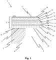
- MEMS transducer 1 shows a detail of a MEMS transducer 1 in cross-section, in particular in the connecting region between a membrane structure 5 and a frame formed as a carrier substrate 2 of the MEMS transducer 1.
- the MEMS transducer is designed to generate and / or detecting sound waves in the audible wavelength spectrum.
- the MEMS sound transducer 1 is thus designed as a MEMS loudspeaker and / or MEMS microphone.
- the MEMS sound transducer 1 comprises a carrier substrate 2, in particular made of silicon.
- the carrier substrate 2 is - as in the in FIG. 2 illustrated embodiment - as, in particular closed, frame formed.
- the carrier substrate 2 accordingly comprises an in FIG. 1 only partially shown cavity 3 or a cavity.
- the cavity 3 comprises a first opening 4, which is spanned by a membrane structure 5.
- the cavity 3 On its side facing away from the membrane structure 5, the cavity 3 has a second opening 6.
- the cavity 3 widens, at least in a region starting from the first opening 4, in the direction of the second opening 6.
- the membrane structure 5 comprises according to FIG. 1 several firmly connected layers. In its edge region 7, the membrane structure 5 is firmly connected to the carrier substrate 2 on its side facing the carrier substrate 2. The membrane structure 5 can thus be compared with the stationary carrier substrate 2 for generating and / or detecting sound energy in the z-direction of the MEMS sound transducer 1, ie according to the in FIG FIG. 1 illustrated orientation in the vertical direction, swing.
- the membrane structure 5 is formed as a multilayer piezoelectric membrane structure.
- the membrane structure 5 accordingly comprises according to the in FIG. 1 illustrated cross-sectional view of a first piezoelectric layer 8 and a second piezoelectric layer 9.
- the two piezoelectric layers 8, 9 need not necessarily be formed continuously over the entire surface of the membrane structure 5. alternative These may also have interruptions, which are explained in more detail in the following embodiments.
- the two piezo layers 8, 9 are preferably made of lead zirconate titanate (PZT) and / or aluminum nitride (ALN).
- PZT lead zirconate titanate
- APN aluminum nitride
- the two piezo layers 8, 9 are each between two electrode layers 10, 11 , 12, 13 embedded.
- the first piezoelectric layer 8 has on its side facing the carrier substrate 2 a first lower electrode layer 10 and on its side remote from the carrier substrate 2 a first upper electrode layer 11.
- a second lower electrode layer 12 is arranged on the second piezoelectric layer 9 on its side facing the carrier substrate 2 and a second upper electrode layer 13 on its side remote from the carrier substrate 2.
- a membrane layer 14 include.
- the membrane layer 14 gives the membrane structure 5 a higher rigidity and / or strength.
- the membrane layer 14 is excited by the two piezo layers 8, 9 to oscillate.
- the membrane layer 14 is preferably made of polysilicon and / or according to the in FIG. 1 illustrated embodiment below the first piezoelectric layer 8, in particular in the region between the first lower electrode layer 10 and the carrier substrate 2, respectively.
- the membrane layer 14 is thus located in the region between the carrier substrate 2 and the lower first piezoelectric layer 8.
- the membrane layer 14 may also be arranged above the second piezoelectric layer 9.
- the Membrane structure 5 completely dispensed with such a membrane layer 14.
- carrier substrate 2 is preferably made of silicon, and is therefore electrically conductive, it is advantageous if the carrier substrate 2 on its side facing the membrane structure 5 an insulating layer 15, in particular of silicon oxide, having. As a result, the first lower electrode layer 10 can be electrically insulated from the carrier substrate 2.
- this has, on its side facing away from the carrier substrate 2, a, in particular uppermost, passivation layer 16.
- the multilayer piezoelectric diaphragm structure 5 described above has a first interface 17 adjacent to the surrounding air. This is located on the side facing away from the carrier substrate 2 side of the membrane structure 5. Furthermore, the membrane structure 5 comprises on its the carrier substrate 2 side facing a second interface 18. Due to the fact that the membrane structure 5, in particular in the region of the two interfaces 17, 18, im Compared to the adjacent air has a very different impedance, a large part of the sound energy to be transmitted at the interface 17, 18 is reflected. As a result, the piezoelectric effect of the MEMS sound transducer 1 is reduced.
- the membrane structure 5 is first vibrated in the z direction via electrical excitation of the two piezo layers 8, 9.
- a sound wave in the audible wavelength spectrum is generated at the first interface 17.
- the sound energy generating sound energy is not completely transferred to the air. Instead, part of the sound energy is due to the large impedance difference between the membrane structure 5 and the adjacent air at the first interface 17 back again, ie in the direction of the carrier substrate 2, reflected. In known from the prior art membrane structure 5, this sound energy is lost, whereby the piezoelectric effect of the membrane structure 5 is reduced.
- the membrane structure 5 therefore according to FIG. 1 a sound energy-reflecting intermediate layer 19.
- the intermediate layer 19 is according to the in FIG. 1 illustrated cross-sectional view in the region between the two piezoelectric layers 8, 9 arranged. In this case, the intermediate layer 19 directly adjoins the first upper electrode layer 11 and the second lower electrode layer 12.
- the intermediate layer 19 has a lower density compared to at least one of the two piezo layers 8, 9. As a result, the intermediate layer 19 and at least one of the two piezo layers 8, 9 have a mutually different impedance. Due to this difference in impedance, the intermediate layer 19 has a sound-reflecting effect. Due to this, the sound application that was previously reflected back at the first interface 17 is reflected by the intermediate layer 19 again in the direction of the first interface 17 using the example of the loudspeaker application. As a result, this sound energy is not lost, but is used again at the interface 17 to generate a sound wave. As a result, the piezoelectric effect of the membrane structure 5 is enhanced.
- the sound energy-reflecting properties of the intermediate layer 19 are particularly pronounced when the intermediate layer 19 consists of silicon oxide, silicon nitride and / or polysilicon.
- the intermediate layer 19 acts on a MEMS sound transducer 1 acting as a microphone.
- the intermediate layer 19 is not only sound-reflecting but also additionally formed dielectrically. As a result, the first upper electrode layer 11 and the second lower electrode layer 12 are electrically mutually distinct isolated. As a result, additional insulation layers can advantageously be saved.
- FIGS. 2, 3 . 4 and 5 In each case different embodiments of the MEMS sound transducer 1 are shown, which do not fall under the claimed protection range.
- Each of these embodiments has, according to the in FIG. 1 shown in detail cutout membrane structure 52 two spaced apart in the z-direction piezoelectric layers 8, 9, which are each sandwiched between two electrode layers 10, 11, 12, 13 are arranged. Furthermore, between these two piezoelectric layers 8, 9 a to the first embodiment identically formed and identically acting intermediate layer 19 is arranged.
- the above-mentioned layer combination represents the basis for the embodiments described below. In the following description of these embodiments, in comparison to the in FIG. 1 illustrated embodiment for the same features same reference numerals. Unless these are explained again in detail, their design and mode of action corresponds to the features already described above.
- the membrane structure 5 no separate membrane layer 14 on. Its effect is instead taken over by the passivation layer 16, which thus acts as a membrane layer 14.
- the passivation layer 16 extends in the horizontal direction over the entire first opening 4.
- the membrane structure 5 indicates the membrane structure 5 according to FIG. 2 on its side facing away from the carrier substrate 2 a plurality of contact recesses 20a, 20b, 20c, 20d.
- the contact recesses 20a, 20b, 20c, 20d extend from the side of the membrane structure 5 facing away from the carrier substrate 2 up to in each case one of the electrode layers 10, 11, 12, 13.
- an electrical connection element 21 in particular an electrical contact arranged in each case.
- the connection element 21 in the in FIG. 2 illustrated embodiment only in one of the contact recesses 20a, 20b, 20c, 20d provided with a reference numeral.
- connection elements 21 are each electrically connected to their associated electrode layer 10, 11, 12, 13. According to the in FIG. 2
- the connection elements 21 extend in each case from the region of the upper side of the membrane structure 5 via the side walls 22 of the respective contact recesses 20a, 20b, 20c, 20d to their base 23.
- an additional insulating layer 15 b is arranged in the region between the connecting element 21 and the side wall 22 in order to ensure that the respective connection elements 21 are provided exclusively with a single electrode layers 10, 11, 12, 12 is electrically connected, in the region between the connecting element 21 and the side wall 22, an additional insulating layer 15 b is arranged.
- the membrane structure 5 has a plurality of recesses 24a, 24b, 24c, 24d.
- the recesses 24a, 24b, 24c, 24d extend from the top of the membrane structure 5 in the direction of the carrier substrate 2.
- the two piezo layers 8, 9 are removed.
- the membrane structure 5 thus has piezoelectric active regions 25 - in which both piezoelectric layers 8, 9 are still present - and piezoelectric passive regions - in which the two piezoelectric layers 8, 9 are removed - (see also FIG. 7 and 8th ).
- FIG. 2 illustrated embodiment only one of these active areas 25 and passive areas 26 provided with a reference numeral.
- the two piezoelectric layers 8, 9, the intermediate layer 19 and all electrode layers 10, 11, 12, 13 are removed.
- the membrane structure 5 thus exclusively the passivation layer 16.
- the passivation layer 16 thus acts as a membrane layer 14.
- the membrane structure 5 in the region of the first opening 4 has a reinforcing layer 27.
- the first insulating layer 15a is not completely removed in the region of the first opening 4.
- this extends in the in FIG. 3 illustrated cross-sectional view horizontally over a plurality, in particular over all, active areas 25 and more, in particular the two inner, passive areas 26.
- the reinforcing layer 27 In its carrier substrate near edge region, the reinforcing layer 27, however, removed.
- the reinforcing layer 27 thus has a spacing in the horizontal direction to the carrier substrate 2, in particular as a frame. The distance is at least such that at least one of the passive regions 26 is formed in the edge region without this reinforcing layer 27.
- the insulating layer 15a arranged in the interior of the carrier substrate 2 designed as a frame thus acts as a reinforcing layer 27.
- the membrane structure 7 is made more stable and / or stiffer.
- the membrane structure 5 is in contrast softer and / or more flexible.
- the reinforcing layer 27 but also be formed by means of the second insulating layer 15b.
- the reinforcing layer 27 or the second insulating layer 15b extends in the horizontal direction over the entire width of the first opening 4.
- the second insulating layer 15b acting as the reinforcing layer 27 may be provided in accordance with FIG. 5 but also in the margins - comparable to the in FIG. 3 illustrated embodiment - be distant.
- the membrane structure 5 has a higher rigidity and / or strength caused by the reinforcing layer 27 only in the inner region.
- the edge region adjoining the carrier substrate 2 is made more flexible and / or softer in comparison since it has no reinforcing layer 27 or second insulating layer 15b.
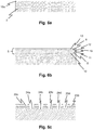
- FIGS. 6a to 6f illustrate the manufacturing process of the MEMS transducer 1 at the in FIG. 5 illustrated embodiment.
- a supporting substrate 2 of silicon is provided with an insulating layer 15a provided on the upper side.
- the membrane structure 5 is applied on top of the insulating layer 15a.
- the first lower electrode layer 10, the first piezo layer 8, the first upper electrode layer 11, the intermediate layer 19, the second lower electrode layer 12, the second piezo layer 9 and the second upper electrode layer 13 are preferably applied one after the other.
- a subsequent process step are according to FIG.
- the contact recesses 20b, 20c, 20d and the recesses 24a, 24b, 24c, 24d are introduced into the membrane structure 5 from the side facing away from the carrier substrate 2.
- the second insulating layer 15b is applied in the contact recesses 20b, 20c, 20d and the two inner recesses 24b, 24c.
- FIG. 6f formed from the underside of the cavity 3, so that the carrier substrate 2 now has a frame shape, against which the membrane structure 5 is able to oscillate in the z direction.
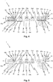
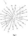
- FIGS. 7 and 8th In each case, two different embodiments of the MEMS sound transducer 1 are shown in a perspective view.
- the Cavity or the cavity 3 is located at this in FIG. 7 and 8th shown perspective view on the back of the MEMS transducer 1 and is therefore not visible.
- the membrane structure 5 and / or not visible here cavity 3 in the plan view is circular. Furthermore, it can be seen in the perspective view that the recesses 24 - of which only one is provided with a reference numeral for the sake of clarity - form a pattern 28.
- the pattern 28 is formed by the piezoelectric active regions 25a, 25b, 25c, 25d and the piezoelectric passive regions 26a, 26b, 26c, 26d, 26e.
- the active region 25a has a rigid and / or firmly clamped first and second armature end 29, 30 connected to the frame or the carrier substrate 2. Furthermore, the active region 25a comprises a free end 31 opposite the two armature ends 29, 30 in the z-direction of deflection. In the region between the respective anchor end 29, 30 and the free end 31, the active region 25a is at least partially substantially meander-shaped.
- the active region 25a starting from the respective armature end 29, 30, has a respective first deflection section 32, a respective second deflection section 33 - only one of which is provided with a reference numeral - and a common third deflection section 34.
- the deflection sections 32, 33, 34 are in the two in FIG. 7 and 8th illustrated embodiments bar-shaped. In each case two mutually adjacent deflection sections 32, 33, 34 are connected to each other by means of a deflection section 35a, 35b. In the present exemplary embodiment, each of the deflection section 35a, 35b deflects the two mutually adjacent deflection sections 32, 33, 34 relative to one another 180 ° around.
- the free ends 31 of the active areas 25a, 25b, 25c, 25d to each other and to a centrally located in the plan view central point 36 at a distance.
- FIG. 8 shows an alternative embodiment of the MEMS sound transducer 1 in perspective view wherein compared to the above in FIG. 7 explained embodiment for the same features same names are used. Unless these are explained again in detail, their design and mode of action corresponds to the features already described above.
- the membrane structure 5 according to the in FIG. 8 illustrated embodiment is not circular but square. Furthermore, the free ends 31 of the respective active regions 25a, 25b, 25c, 25d lie directly against one another in the central point 36. Additionally or alternatively, however, the free ends 31 can also be connected to one another and / or formed integrally with one another.
- FIG. 9 shows a cross section through an active area 25, in particular by a bar-shaped deflection section 32, 33, 34 and / or deflection section 35a, 35b one of in FIG. 7 and / or 8 illustrated embodiments.
- the second upper electrode layer 13 is arranged asymmetrically with respect to the second piezo layer 9.
- the active region 25 is twisted around its longitudinal axis, as a result of which the maximum lifting height in the z direction of the MEMS sound transducer 1 can be increased. This twist is in FIG. 9 indicated by an arrow.
- too Further or all electrode layers 10, 11, 12, 13 with respect to their respective associated piezoelectric layer 8, 9 may be arranged asymmetrically.
- the MEMS sound transducer 1 can according to FIG. 10 be arranged in an array 37. According to the in FIG. 10 illustrated embodiment, all MEMS sound transducer 1 have the same shape and size. Furthermore, their active region 25 each has the same pattern 28. In an alternative embodiment not shown here, these MEMS sound transducers 1 arranged in the manner of an array may also have different sizes relative to one another. As a result, high and woofers can be formed. Furthermore, the MEMS sound transducers 1 may have different patterns 28 and membrane structure shapes from each other. According to the in FIG.
- the MEMS transducer 1 comprises at least two, in particular separately controllable, transducer regions 38, 39, the transducer regions 38, 39 of the one-piece membrane structure 5 may be formed differently sized and / or have different patterns.
- the MEMS sound transducer 1 has at least one support element 40 in the interior of the frame or the carrier substrate 2.
- the support member 40 is formed as a wall and divides the cavity 3 into a first and second cavity portion 41, 42. According to the present, not covered by the claimed scope.
- the support member 40 may be spaced with its the diaphragm structure 5 facing support member end 43 in the z-direction thereof.
- the support member 40 with its Stützelementendet 43 directly, in particular loosely, rests against the underside of the membrane structure 5 or, as claimed according to the invention, is firmly connected thereto.
- the present invention is not limited to the illustrated and described embodiments. Variations within the scope of the claims are possible. A combination of the features is possible, even if they are shown and described in different embodiments.
Landscapes
- Engineering & Computer Science (AREA)
- Physics & Mathematics (AREA)
- Acoustics & Sound (AREA)
- Signal Processing (AREA)
- Multimedia (AREA)
- Piezo-Electric Transducers For Audible Bands (AREA)
- Micromachines (AREA)
- Electrostatic, Electromagnetic, Magneto- Strictive, And Variable-Resistance Transducers (AREA)
Claims (13)
- Transducteur acoustique MEMS pour générer et/ou détecter des ondes acoustiques dans le spectre de longueur d'onde audible, avec
un substrat support (2),
un espace vide (3) formé dans le substrat support (2), lequel présente au moins une ouverture (4), et
une structure de membrane piézoélectrique multicouche (5) qui s'étend sur l'ouverture (4) de l'espace creux (3) et qui est reliée dans sa zone de bordure avec le substrat support (2) de manière à pouvoir osciller par rapport au substrat support (2) pour générer et/ou détecter l'énergie acoustique,
dans lequel la structure de membrane (5) comporte au moins en certaines zones de sa section transversale une première couche piézoélectrique et une seconde couche piézoélectrique (8, 9) disposée à distance de la première couche piézoélectrique (8), et
dans laquelle une couche intermédiaire (19) est disposée dans la zone entre les deux couches piézoélectriques (8, 9),
laquelle se présente sous une forme telle que, avec son aide, l'énergie acoustique puis être réfléchie dans la direction d'au moins une surface interfaciale (17, 18) de la structure de membrane (5) mitoyenne à l'air,
caractérisé en ce que
la structure de membrane (5) présente, en vue de dessus, une multitude de zones de transducteurs (38, 39) pouvant être actionnées séparément les unes des autres,
le substrat support (2) présente, en vue de dessus, au moins un élément de soutien (40) formé à l'intérieur du cadre, qui est disposé entre deux zones de transducteurs (38, 39) afin de supporter la structure de membrane (5), et en ce que
l'élément de soutien (40) est relié avec la structure de membrane (5) par son extrémité (43) d'élément de soutien orientée vers la structure de membrane (5). - Transducteur acoustique MEMS selon la revendication précédente, caractérisé en ce que la couche intermédiaire (19) présente une densité plus faible par comparaison avec au moins l'une des deux couches piézoélectriques (8, 9).
- Transducteur acoustique MEMS selon l'une ou plusieurs des revendications précédentes, caractérisé en ce que la couche intermédiaire (19) est fabriquée en oxyde de silicium, nitrure de silicium et/ou polysilicium.
- Transducteur acoustique MEMS selon l'une ou plusieurs des revendications précédentes, caractérisé en ce que l'une au moins des deux couches piézoélectriques (8, 9) est fabriqué en titano-zirconate de plomb et/ou nitrure d'aluminium.
- Transducteur acoustique MEMS selon l'une ou plusieurs des revendications précédentes, caractérisé en ce que les deux couches piézoélectriques (8, 9) sont respectivement incorporées entre une couche d'électrode supérieure et une couche d'électrode inférieures (10, 12; 11, 13),
que la couche intermédiaire (19) est en contact direct avec la couche d'électrode supérieure (11) de la première couche piézoélectrique (8) et la couche d'électrode inférieure (12) de la seconde couche piézoélectrique (9) et/ou en ce que la couche intermédiaire (19) se présente sous une forme diélectrique. - Transducteur acoustique MEMS selon l'une ou plusieurs des revendications précédentes, caractérisé en ce que la structure de membrane (5) comporte une couche de membrane (14) qui est disposée dans la zone au-dessous de la première couche piézoélectrique (8) ou dans la zone au-dessus de la seconde couche piézoélectrique (9).
- Transducteur acoustique MEMS selon l'une ou plusieurs des revendications précédentes, caractérisé en ce que la structure de membrane (5) présente au moins un évidement (24) dans la zone duquel au moins les deux couches piézoélectriques (8, 9) sont enlevées, de sorte que la structure de membrane (5) présente, en vue de dessus, au moins une zone active piézoélectrique (25) et au moins une zone passive (26) formée par l'évidement (24).
- Transducteur acoustique MEMS selon la revendication 7, caractérisé en ce que l'évidement (24) se présente sous une forme telle que la zone active piézoélectrique (25) présente, en vue de dessus, au moins une extrémité d'ancrage (29, 30) reliée au cadre et au moins une extrémité libre (31) pouvant osciller par rapport à cette dernière dans la direction z.
- Transducteur acoustique MEMS selon l'une ou plusieurs des revendications 7 ou 8, caractérisé en ce que la zone active (25) présente en vue de dessus au moins une section de déviation (32, 33, 34) et/ou que, dans sa vue en coupe transversale, et dans au moins l'une de ses deux couches piézoélectriques (8, 9), au moins une des deux couches d'électrode (10, 11, 12, 13) est disposée asymétriquement par rapport à la couche piézoélectrique (8, 9) qui lui correspond.
- Transducteur acoustique MEMS selon l'une ou plusieurs des revendications 7 à 9, caractérisé en ce que la zone active (25) présente en vue de dessus au moins une première section de déviation (32), une seconde section de déviation (33) et/ou une section de renvoi (35) formée entre les deux sections citées.
- Transducteur acoustique MEMS selon l'une ou plusieurs des revendications précédentes, caractérisé en ce que les zones de transducteurs (38, 39) présentent des tailles différentes et/ou des motifs différents (28).
- Transducteur acoustique MEMS selon l'une ou plusieurs des revendications précédentes, caractérisé en ce que l'élément de soutien (40) se présente sous la forme d'une paroi et subdivise l'espace creux (3) en au moins deux zones (41, 42) d'espace creux.
- Puce pour générer et/ou détecter des ondes acoustiques dans le spectre de longueur d'onde audible, avec plusieurs transducteurs acoustiques MEMS (1) disposés en réseau les uns par rapport aux autres et/ou pouvant être actionnés séparément les uns des autres, caractérisée en ce que l'un au moins des transducteurs acoustiques MEMS (1) se présente sous une forme selon l'une ou plusieurs des revendications précédentes.
Applications Claiming Priority (2)
| Application Number | Priority Date | Filing Date | Title |
|---|---|---|---|
| DE102013114826.3A DE102013114826A1 (de) | 2013-12-23 | 2013-12-23 | Mikro-elektromechanischer Schallwandler mit schallenergiereflektierender Zwischenschicht |
| PCT/EP2014/078220 WO2015097035A1 (fr) | 2013-12-23 | 2014-12-17 | Transducteur acoustique microélectromécanique avec couche intermédiaire réfléchissant l'énergie acoustique |
Publications (2)
| Publication Number | Publication Date |
|---|---|
| EP3087760A1 EP3087760A1 (fr) | 2016-11-02 |
| EP3087760B1 true EP3087760B1 (fr) | 2019-03-13 |
Family
ID=52232168
Family Applications (1)
| Application Number | Title | Priority Date | Filing Date |
|---|---|---|---|
| EP14820823.4A Active EP3087760B1 (fr) | 2013-12-23 | 2014-12-17 | Transducteur acoustique microélectromécanique avec couche intermédiaire réfléchissant l'énergie acoustique |
Country Status (10)
| Country | Link |
|---|---|
| US (1) | US10045125B2 (fr) |
| EP (1) | EP3087760B1 (fr) |
| KR (1) | KR102208617B1 (fr) |
| CN (1) | CN106416295B (fr) |
| AU (1) | AU2014372721B2 (fr) |
| CA (1) | CA2934994A1 (fr) |
| DE (1) | DE102013114826A1 (fr) |
| MY (1) | MY177541A (fr) |
| SG (1) | SG11201605179XA (fr) |
| WO (1) | WO2015097035A1 (fr) |
Cited By (1)
| Publication number | Priority date | Publication date | Assignee | Title |
|---|---|---|---|---|
| US20230081056A1 (en) * | 2021-09-16 | 2023-03-16 | Skyworks Solutions, Inc. | Acoustic device with connected cantilever |
Families Citing this family (20)
| Publication number | Priority date | Publication date | Assignee | Title |
|---|---|---|---|---|
| DE102015114242A1 (de) * | 2015-08-27 | 2017-03-02 | USound GmbH | MEMS-Lautsprecher mit Positionssensor |
| DE102015116707A1 (de) * | 2015-10-01 | 2017-04-06 | USound GmbH | Flexible MEMS-Leiterplatteneinheit sowie Schallwandleranordnung |
| DE102015116640B4 (de) | 2015-10-01 | 2024-09-05 | USound GmbH | MEMS-Leiterplattenmodul mit integrierter piezoelektrischer Struktur sowie Schallwandleranordnung |
| JP7067891B2 (ja) * | 2017-10-18 | 2022-05-16 | Mmiセミコンダクター株式会社 | トランスデューサ |
| EP3676025B1 (fr) | 2017-11-16 | 2024-08-14 | InvenSense, Inc. | Transducteur ultrasonore micro-usiné piézoélectrique avec une structure de membrane à motifs, et une méthode de fabrication |
| US11256818B2 (en) | 2017-12-28 | 2022-02-22 | Corlina, Inc. | System and method for enabling and verifying the trustworthiness of a hardware system |
| WO2019152521A1 (fr) | 2018-01-30 | 2019-08-08 | Corlina, Inc. | Intégration d'utilisateur et de dispositif |
| DE102018203812A1 (de) * | 2018-03-13 | 2019-09-19 | Christian-Albrechts-Universität Zu Kiel | Ferroelektrisches material, mems-bauteil mit einem ferroelektrischen material, mems-vorrichtung mit einem ersten mems-bauteil, verfahren zur herstellung eines mems-bauteils und verfahren zur herstellung eines cmos-kompatiblen mems-bauteils |
| EP3620429B1 (fr) * | 2018-09-06 | 2025-05-21 | Infineon Technologies AG | Transducteur mems a membrane et son procede de fabrication |
| CN112423210A (zh) * | 2019-08-21 | 2021-02-26 | 新科实业有限公司 | Mems换能器、mems麦克风以及制造mems换能器的方法 |
| DE112020004374T5 (de) * | 2019-09-13 | 2022-07-21 | Rohm Co., Ltd. | Wandler |
| EP4058400B1 (fr) * | 2019-11-13 | 2025-09-10 | Fraunhofer-Gesellschaft zur Förderung der angewandten Forschung e.V. | Composant mems comprenant un élément mobile dans le plan |
| KR102367922B1 (ko) | 2019-11-29 | 2022-02-25 | 국방과학연구소 | 압전 멤스 벡터 하이드로폰 및 이의 제조 방법 |
| DE102021203360A1 (de) * | 2021-04-01 | 2022-10-06 | Fraunhofer-Gesellschaft zur Förderung der angewandten Forschung eingetragener Verein | Mems-schallwandler |
| TWI803124B (zh) | 2021-12-29 | 2023-05-21 | 財團法人工業技術研究院 | 具多重振動部的微機電裝置 |
| US12238478B2 (en) | 2022-01-18 | 2025-02-25 | Taiwan Semiconductor Manufacturing Company, Ltd. | Top notch slit profile for MEMS device |
| EP4236367A1 (fr) * | 2022-02-28 | 2023-08-30 | Hahn-Schickard-Gesellschaft für angewandte Forschung e.V. | Ondulations ou zones d'affaiblissement sur les structures d'ancrage des membranes transductrices mems verticales |
| US20250184667A1 (en) * | 2022-02-28 | 2025-06-05 | Hahn-Schickard-Gesellschaft Für Angewandte Forschung E. V. | Corrugations or weakened regions on armature structures of vertical mems converter membranes |
| CN116761124A (zh) * | 2022-03-03 | 2023-09-15 | 华为技术有限公司 | 压电mems麦克风和电子设备 |
| TWI828327B (zh) * | 2022-09-22 | 2024-01-01 | 國立臺灣大學 | 寬頻高音質的壓電材料複合振膜聲學元件及其製造方法 |
Citations (1)
| Publication number | Priority date | Publication date | Assignee | Title |
|---|---|---|---|---|
| US20110120843A1 (en) * | 2008-06-19 | 2011-05-26 | Nxp B.V. | Piezoelectric bimorph switch |
Family Cites Families (17)
| Publication number | Priority date | Publication date | Assignee | Title |
|---|---|---|---|---|
| US4861420A (en) | 1984-06-04 | 1989-08-29 | Tactile Perceptions, Inc. | Method of making a semiconductor transducer |
| US5650685A (en) * | 1992-01-30 | 1997-07-22 | The United States Of America As Represented By The Secretary Of The Army | Microcircuit package with integrated acoustic isolator |
| AU2923397A (en) * | 1996-04-18 | 1997-11-07 | California Institute Of Technology | Thin film electret microphone |
| DE102005008512B4 (de) | 2005-02-24 | 2016-06-23 | Epcos Ag | Elektrisches Modul mit einem MEMS-Mikrofon |
| DE102005008511B4 (de) | 2005-02-24 | 2019-09-12 | Tdk Corporation | MEMS-Mikrofon |
| DE102005008514B4 (de) * | 2005-02-24 | 2019-05-16 | Tdk Corporation | Mikrofonmembran und Mikrofon mit der Mikrofonmembran |
| US20080149832A1 (en) * | 2006-12-20 | 2008-06-26 | Miguel Zorn | Scanning Probe Microscope, Nanomanipulator with Nanospool, Motor, nucleotide cassette and Gaming application |
| JP2009010559A (ja) * | 2007-06-27 | 2009-01-15 | Nippon Dempa Kogyo Co Ltd | 圧電部品及びその製造方法 |
| JP2009260723A (ja) * | 2008-04-17 | 2009-11-05 | Asahi Kasei Electronics Co Ltd | トランスデューサ |
| KR101606780B1 (ko) | 2008-06-30 | 2016-03-28 | 더 리젠츠 오브 더 유니버시티 오브 미시건 | 압전 mems 마이크로폰 |
| DE102009002986B4 (de) * | 2009-05-11 | 2022-07-14 | Robert Bosch Gmbh | Piezoelektrischer Energiewandler mit Anschlag und Verfahren zur Herstellung |
| KR101561661B1 (ko) | 2009-09-25 | 2015-10-21 | 삼성전자주식회사 | 진동막에 부착된 질량체를 가진 압전형 마이크로 스피커 및 그 제조 방법 |
| JP5385117B2 (ja) * | 2009-12-17 | 2014-01-08 | 富士フイルム株式会社 | 圧電memsスイッチの製造方法 |
| JP2012080165A (ja) * | 2010-09-30 | 2012-04-19 | Yamaha Corp | コンデンサマイクロホンアレイチップ |
| US8724832B2 (en) | 2011-08-30 | 2014-05-13 | Qualcomm Mems Technologies, Inc. | Piezoelectric microphone fabricated on glass |
| US8496842B2 (en) * | 2011-09-12 | 2013-07-30 | Texas Instruments Incorporated | MEMS device fabricated with integrated circuit |
| US9402137B2 (en) | 2011-11-14 | 2016-07-26 | Infineon Technologies Ag | Sound transducer with interdigitated first and second sets of comb fingers |
-
2013
- 2013-12-23 DE DE102013114826.3A patent/DE102013114826A1/de not_active Withdrawn
-
2014
- 2014-12-17 MY MYPI2016702313A patent/MY177541A/en unknown
- 2014-12-17 CA CA2934994A patent/CA2934994A1/fr not_active Abandoned
- 2014-12-17 SG SG11201605179XA patent/SG11201605179XA/en unknown
- 2014-12-17 WO PCT/EP2014/078220 patent/WO2015097035A1/fr not_active Ceased
- 2014-12-17 US US15/107,371 patent/US10045125B2/en active Active
- 2014-12-17 CN CN201480070788.1A patent/CN106416295B/zh active Active
- 2014-12-17 EP EP14820823.4A patent/EP3087760B1/fr active Active
- 2014-12-17 KR KR1020167019823A patent/KR102208617B1/ko not_active Expired - Fee Related
- 2014-12-17 AU AU2014372721A patent/AU2014372721B2/en not_active Ceased
Patent Citations (1)
| Publication number | Priority date | Publication date | Assignee | Title |
|---|---|---|---|---|
| US20110120843A1 (en) * | 2008-06-19 | 2011-05-26 | Nxp B.V. | Piezoelectric bimorph switch |
Non-Patent Citations (1)
| Title |
|---|
| "Microsystems and Nanotechnologie", 30 August 2012, SPRINGER BERLIN HEIDELBERG, ISBN: 978-3-642-18292-1, article ZHAOYING ZHOU ET AL: "Structure Materials for Microsystems (Chapter 3.3)", pages: 89 - 105, XP055386766 * |
Cited By (2)
| Publication number | Priority date | Publication date | Assignee | Title |
|---|---|---|---|---|
| US20230081056A1 (en) * | 2021-09-16 | 2023-03-16 | Skyworks Solutions, Inc. | Acoustic device with connected cantilever |
| US12302063B2 (en) * | 2021-09-16 | 2025-05-13 | Skyworks Solutions, Inc. | Acoustic device with connected cantilever |
Also Published As
| Publication number | Publication date |
|---|---|
| CN106416295B (zh) | 2020-01-03 |
| SG11201605179XA (en) | 2016-08-30 |
| US10045125B2 (en) | 2018-08-07 |
| DE102013114826A1 (de) | 2015-06-25 |
| AU2014372721A1 (en) | 2016-07-28 |
| CA2934994A1 (fr) | 2015-07-02 |
| CN106416295A (zh) | 2017-02-15 |
| KR20160114068A (ko) | 2016-10-04 |
| WO2015097035A1 (fr) | 2015-07-02 |
| KR102208617B1 (ko) | 2021-01-28 |
| US20170006381A1 (en) | 2017-01-05 |
| MY177541A (en) | 2020-09-18 |
| AU2014372721B2 (en) | 2018-11-08 |
| EP3087760A1 (fr) | 2016-11-02 |
Similar Documents
| Publication | Publication Date | Title |
|---|---|---|
| EP3087760A1 (fr) | Transducteur acoustique microélectromécanique avec couche intermédiaire réfléchissant l'énergie acoustique | |
| EP3701728B1 (fr) | Ensemble formant transducteur acoustique | |
| EP3143778B1 (fr) | Transducteur acoustique mems ainsi que système de transducteur acoustique équipé d'un mécanisme d'arrêt | |
| EP3381202B1 (fr) | Unité carte de circuit imprimé mems souple et ensemble transducteur acoustique | |
| DE69635308T2 (de) | Piezoelektrischer wandler | |
| DE102017115923B4 (de) | Mikroelektromechanischer Transducer | |
| EP3852391A1 (fr) | Haut-parleurs mems ayant une efficacité accrue | |
| DE102014105754B4 (de) | Lautsprecheranordnung mit leiterplattenintegriertem ASIC | |
| EP3590271A1 (fr) | Unité haut-parleur dotée d'un haut-parleur électrodynamique et d'un haut-parleur mems | |
| WO2016034665A1 (fr) | Mems comprenant des actionneurs piézoélectriques micromécaniques pour obtenir des forces et des déflexions élevées | |
| DE102006007494A1 (de) | Ultraschallelement | |
| EP3136751A1 (fr) | Haut-parleur mems avec capteur de position | |
| EP3799966B1 (fr) | Convertisseur acoustique et procédé de génération/réception d'une onde acoustique | |
| DE102020123366A1 (de) | Ringförmig strahlende Lautsprecherboxstruktur | |
| DE102015213757A1 (de) | Mikromechanische Struktur und Verfahren zur Herstellung derselben | |
| DE102021202573B3 (de) | Mems-schallwandler mit ausnehmungen und auskragungen | |
| EP3739904B1 (fr) | Système de transducteur acoustique et dispositif acoustique | |
| EP4315882B1 (fr) | Transducteur acoustique mems | |
| DE102013105557B4 (de) | Piezoelektrischer Aktor | |
| DE4135408A1 (de) | Verfahren zur umwandlung elektrischer energie in mechanische schwingungen, sowie vorrichtungen zur durchfuehrung dieses verfahrens | |
| DE10013673C2 (de) | Mikromechanischer elektroakustischer Wandler | |
| DE102024204501A1 (de) | Mikro-elektro-mechanisches Schwingungssystem | |
| DE102022210125A1 (de) | Mikromechanische Schallwandlervorrichtung und entsprechendes Schallwandlungsverfahren | |
| DE112006001232T5 (de) | Lautsprecherbox und Lautsprechervorrichtung | |
| DE102023125386A1 (de) | MEMS-Schallwandler und dessen Herstellungsverfahren |
Legal Events
| Date | Code | Title | Description |
|---|---|---|---|
| PUAI | Public reference made under article 153(3) epc to a published international application that has entered the european phase |
Free format text: ORIGINAL CODE: 0009012 |
|
| 17P | Request for examination filed |
Effective date: 20160720 |
|
| AK | Designated contracting states |
Kind code of ref document: A1 Designated state(s): AL AT BE BG CH CY CZ DE DK EE ES FI FR GB GR HR HU IE IS IT LI LT LU LV MC MK MT NL NO PL PT RO RS SE SI SK SM TR |
|
| AX | Request for extension of the european patent |
Extension state: BA ME |
|
| DAX | Request for extension of the european patent (deleted) | ||
| STAA | Information on the status of an ep patent application or granted ep patent |
Free format text: STATUS: EXAMINATION IS IN PROGRESS |
|
| 17Q | First examination report despatched |
Effective date: 20170706 |
|
| RIN1 | Information on inventor provided before grant (corrected) |
Inventor name: RUSCONI CLERICI, ANDREA Inventor name: BOTTONI, FERRUCCIO |
|
| RAP1 | Party data changed (applicant data changed or rights of an application transferred) |
Owner name: USOUND GMBH |
|
| GRAP | Despatch of communication of intention to grant a patent |
Free format text: ORIGINAL CODE: EPIDOSNIGR1 |
|
| STAA | Information on the status of an ep patent application or granted ep patent |
Free format text: STATUS: GRANT OF PATENT IS INTENDED |
|
| INTG | Intention to grant announced |
Effective date: 20181004 |
|
| RIN1 | Information on inventor provided before grant (corrected) |
Inventor name: RUSCONI CLERICI BELTRAMI, ANDREA Inventor name: BOTTONI, FERRUCCIO |
|
| GRAS | Grant fee paid |
Free format text: ORIGINAL CODE: EPIDOSNIGR3 |
|
| GRAA | (expected) grant |
Free format text: ORIGINAL CODE: 0009210 |
|
| STAA | Information on the status of an ep patent application or granted ep patent |
Free format text: STATUS: THE PATENT HAS BEEN GRANTED |
|
| AK | Designated contracting states |
Kind code of ref document: B1 Designated state(s): AL AT BE BG CH CY CZ DE DK EE ES FI FR GB GR HR HU IE IS IT LI LT LU LV MC MK MT NL NO PL PT RO RS SE SI SK SM TR |
|
| REG | Reference to a national code |
Ref country code: GB Ref legal event code: FG4D Free format text: NOT ENGLISH |
|
| REG | Reference to a national code |
Ref country code: CH Ref legal event code: EP Ref country code: AT Ref legal event code: REF Ref document number: 1109338 Country of ref document: AT Kind code of ref document: T Effective date: 20190315 |
|
| REG | Reference to a national code |
Ref country code: IE Ref legal event code: FG4D Free format text: LANGUAGE OF EP DOCUMENT: GERMAN |
|
| REG | Reference to a national code |
Ref country code: DE Ref legal event code: R096 Ref document number: 502014011149 Country of ref document: DE |
|
| REG | Reference to a national code |
Ref country code: NL Ref legal event code: MP Effective date: 20190313 |
|
| REG | Reference to a national code |
Ref country code: LT Ref legal event code: MG4D |
|
| PG25 | Lapsed in a contracting state [announced via postgrant information from national office to epo] |
Ref country code: NO Free format text: LAPSE BECAUSE OF FAILURE TO SUBMIT A TRANSLATION OF THE DESCRIPTION OR TO PAY THE FEE WITHIN THE PRESCRIBED TIME-LIMIT Effective date: 20190613 Ref country code: LT Free format text: LAPSE BECAUSE OF FAILURE TO SUBMIT A TRANSLATION OF THE DESCRIPTION OR TO PAY THE FEE WITHIN THE PRESCRIBED TIME-LIMIT Effective date: 20190313 Ref country code: FI Free format text: LAPSE BECAUSE OF FAILURE TO SUBMIT A TRANSLATION OF THE DESCRIPTION OR TO PAY THE FEE WITHIN THE PRESCRIBED TIME-LIMIT Effective date: 20190313 Ref country code: SE Free format text: LAPSE BECAUSE OF FAILURE TO SUBMIT A TRANSLATION OF THE DESCRIPTION OR TO PAY THE FEE WITHIN THE PRESCRIBED TIME-LIMIT Effective date: 20190313 |
|
| PG25 | Lapsed in a contracting state [announced via postgrant information from national office to epo] |
Ref country code: BG Free format text: LAPSE BECAUSE OF FAILURE TO SUBMIT A TRANSLATION OF THE DESCRIPTION OR TO PAY THE FEE WITHIN THE PRESCRIBED TIME-LIMIT Effective date: 20190613 Ref country code: HR Free format text: LAPSE BECAUSE OF FAILURE TO SUBMIT A TRANSLATION OF THE DESCRIPTION OR TO PAY THE FEE WITHIN THE PRESCRIBED TIME-LIMIT Effective date: 20190313 Ref country code: LV Free format text: LAPSE BECAUSE OF FAILURE TO SUBMIT A TRANSLATION OF THE DESCRIPTION OR TO PAY THE FEE WITHIN THE PRESCRIBED TIME-LIMIT Effective date: 20190313 Ref country code: GR Free format text: LAPSE BECAUSE OF FAILURE TO SUBMIT A TRANSLATION OF THE DESCRIPTION OR TO PAY THE FEE WITHIN THE PRESCRIBED TIME-LIMIT Effective date: 20190614 Ref country code: RS Free format text: LAPSE BECAUSE OF FAILURE TO SUBMIT A TRANSLATION OF THE DESCRIPTION OR TO PAY THE FEE WITHIN THE PRESCRIBED TIME-LIMIT Effective date: 20190313 Ref country code: NL Free format text: LAPSE BECAUSE OF FAILURE TO SUBMIT A TRANSLATION OF THE DESCRIPTION OR TO PAY THE FEE WITHIN THE PRESCRIBED TIME-LIMIT Effective date: 20190313 |
|
| PG25 | Lapsed in a contracting state [announced via postgrant information from national office to epo] |
Ref country code: IT Free format text: LAPSE BECAUSE OF FAILURE TO SUBMIT A TRANSLATION OF THE DESCRIPTION OR TO PAY THE FEE WITHIN THE PRESCRIBED TIME-LIMIT Effective date: 20190313 Ref country code: RO Free format text: LAPSE BECAUSE OF FAILURE TO SUBMIT A TRANSLATION OF THE DESCRIPTION OR TO PAY THE FEE WITHIN THE PRESCRIBED TIME-LIMIT Effective date: 20190313 Ref country code: SK Free format text: LAPSE BECAUSE OF FAILURE TO SUBMIT A TRANSLATION OF THE DESCRIPTION OR TO PAY THE FEE WITHIN THE PRESCRIBED TIME-LIMIT Effective date: 20190313 Ref country code: CZ Free format text: LAPSE BECAUSE OF FAILURE TO SUBMIT A TRANSLATION OF THE DESCRIPTION OR TO PAY THE FEE WITHIN THE PRESCRIBED TIME-LIMIT Effective date: 20190313 Ref country code: ES Free format text: LAPSE BECAUSE OF FAILURE TO SUBMIT A TRANSLATION OF THE DESCRIPTION OR TO PAY THE FEE WITHIN THE PRESCRIBED TIME-LIMIT Effective date: 20190313 Ref country code: PT Free format text: LAPSE BECAUSE OF FAILURE TO SUBMIT A TRANSLATION OF THE DESCRIPTION OR TO PAY THE FEE WITHIN THE PRESCRIBED TIME-LIMIT Effective date: 20190713 Ref country code: EE Free format text: LAPSE BECAUSE OF FAILURE TO SUBMIT A TRANSLATION OF THE DESCRIPTION OR TO PAY THE FEE WITHIN THE PRESCRIBED TIME-LIMIT Effective date: 20190313 Ref country code: AL Free format text: LAPSE BECAUSE OF FAILURE TO SUBMIT A TRANSLATION OF THE DESCRIPTION OR TO PAY THE FEE WITHIN THE PRESCRIBED TIME-LIMIT Effective date: 20190313 |
|
| PG25 | Lapsed in a contracting state [announced via postgrant information from national office to epo] |
Ref country code: SM Free format text: LAPSE BECAUSE OF FAILURE TO SUBMIT A TRANSLATION OF THE DESCRIPTION OR TO PAY THE FEE WITHIN THE PRESCRIBED TIME-LIMIT Effective date: 20190313 Ref country code: PL Free format text: LAPSE BECAUSE OF FAILURE TO SUBMIT A TRANSLATION OF THE DESCRIPTION OR TO PAY THE FEE WITHIN THE PRESCRIBED TIME-LIMIT Effective date: 20190313 |
|
| REG | Reference to a national code |
Ref country code: DE Ref legal event code: R097 Ref document number: 502014011149 Country of ref document: DE |
|
| PG25 | Lapsed in a contracting state [announced via postgrant information from national office to epo] |
Ref country code: IS Free format text: LAPSE BECAUSE OF FAILURE TO SUBMIT A TRANSLATION OF THE DESCRIPTION OR TO PAY THE FEE WITHIN THE PRESCRIBED TIME-LIMIT Effective date: 20190713 |
|
| PLBE | No opposition filed within time limit |
Free format text: ORIGINAL CODE: 0009261 |
|
| STAA | Information on the status of an ep patent application or granted ep patent |
Free format text: STATUS: NO OPPOSITION FILED WITHIN TIME LIMIT |
|
| PG25 | Lapsed in a contracting state [announced via postgrant information from national office to epo] |
Ref country code: DK Free format text: LAPSE BECAUSE OF FAILURE TO SUBMIT A TRANSLATION OF THE DESCRIPTION OR TO PAY THE FEE WITHIN THE PRESCRIBED TIME-LIMIT Effective date: 20190313 |
|
| 26N | No opposition filed |
Effective date: 20191216 |
|
| PG25 | Lapsed in a contracting state [announced via postgrant information from national office to epo] |
Ref country code: SI Free format text: LAPSE BECAUSE OF FAILURE TO SUBMIT A TRANSLATION OF THE DESCRIPTION OR TO PAY THE FEE WITHIN THE PRESCRIBED TIME-LIMIT Effective date: 20190313 |
|
| PG25 | Lapsed in a contracting state [announced via postgrant information from national office to epo] |
Ref country code: TR Free format text: LAPSE BECAUSE OF FAILURE TO SUBMIT A TRANSLATION OF THE DESCRIPTION OR TO PAY THE FEE WITHIN THE PRESCRIBED TIME-LIMIT Effective date: 20190313 |
|
| REG | Reference to a national code |
Ref country code: BE Ref legal event code: MM Effective date: 20191231 |
|
| PG25 | Lapsed in a contracting state [announced via postgrant information from national office to epo] |
Ref country code: MC Free format text: LAPSE BECAUSE OF FAILURE TO SUBMIT A TRANSLATION OF THE DESCRIPTION OR TO PAY THE FEE WITHIN THE PRESCRIBED TIME-LIMIT Effective date: 20190313 |
|
| PG25 | Lapsed in a contracting state [announced via postgrant information from national office to epo] |
Ref country code: IE Free format text: LAPSE BECAUSE OF NON-PAYMENT OF DUE FEES Effective date: 20191217 Ref country code: LU Free format text: LAPSE BECAUSE OF NON-PAYMENT OF DUE FEES Effective date: 20191217 |
|
| PG25 | Lapsed in a contracting state [announced via postgrant information from national office to epo] |
Ref country code: BE Free format text: LAPSE BECAUSE OF NON-PAYMENT OF DUE FEES Effective date: 20191231 |
|
| PG25 | Lapsed in a contracting state [announced via postgrant information from national office to epo] |
Ref country code: CY Free format text: LAPSE BECAUSE OF FAILURE TO SUBMIT A TRANSLATION OF THE DESCRIPTION OR TO PAY THE FEE WITHIN THE PRESCRIBED TIME-LIMIT Effective date: 20190313 |
|
| PG25 | Lapsed in a contracting state [announced via postgrant information from national office to epo] |
Ref country code: MT Free format text: LAPSE BECAUSE OF FAILURE TO SUBMIT A TRANSLATION OF THE DESCRIPTION OR TO PAY THE FEE WITHIN THE PRESCRIBED TIME-LIMIT Effective date: 20190313 Ref country code: HU Free format text: LAPSE BECAUSE OF FAILURE TO SUBMIT A TRANSLATION OF THE DESCRIPTION OR TO PAY THE FEE WITHIN THE PRESCRIBED TIME-LIMIT; INVALID AB INITIO Effective date: 20141217 |
|
| PG25 | Lapsed in a contracting state [announced via postgrant information from national office to epo] |
Ref country code: MK Free format text: LAPSE BECAUSE OF FAILURE TO SUBMIT A TRANSLATION OF THE DESCRIPTION OR TO PAY THE FEE WITHIN THE PRESCRIBED TIME-LIMIT Effective date: 20190313 |
|
| PGFP | Annual fee paid to national office [announced via postgrant information from national office to epo] |
Ref country code: GB Payment date: 20221215 Year of fee payment: 9 Ref country code: FR Payment date: 20221216 Year of fee payment: 9 Ref country code: AT Payment date: 20221216 Year of fee payment: 9 |
|
| PGFP | Annual fee paid to national office [announced via postgrant information from national office to epo] |
Ref country code: CH Payment date: 20221229 Year of fee payment: 9 |
|
| P01 | Opt-out of the competence of the unified patent court (upc) registered |
Effective date: 20230417 |
|
| REG | Reference to a national code |
Ref country code: CH Ref legal event code: PL |
|
| REG | Reference to a national code |
Ref country code: AT Ref legal event code: MM01 Ref document number: 1109338 Country of ref document: AT Kind code of ref document: T Effective date: 20231217 |
|
| GBPC | Gb: european patent ceased through non-payment of renewal fee |
Effective date: 20231217 |
|
| PG25 | Lapsed in a contracting state [announced via postgrant information from national office to epo] |
Ref country code: GB Free format text: LAPSE BECAUSE OF NON-PAYMENT OF DUE FEES Effective date: 20231217 |
|
| PG25 | Lapsed in a contracting state [announced via postgrant information from national office to epo] |
Ref country code: FR Free format text: LAPSE BECAUSE OF NON-PAYMENT OF DUE FEES Effective date: 20231231 |
|
| PG25 | Lapsed in a contracting state [announced via postgrant information from national office to epo] |
Ref country code: CH Free format text: LAPSE BECAUSE OF NON-PAYMENT OF DUE FEES Effective date: 20231231 |
|
| PG25 | Lapsed in a contracting state [announced via postgrant information from national office to epo] |
Ref country code: AT Free format text: LAPSE BECAUSE OF NON-PAYMENT OF DUE FEES Effective date: 20231217 |
|
| PG25 | Lapsed in a contracting state [announced via postgrant information from national office to epo] |
Ref country code: GB Free format text: LAPSE BECAUSE OF NON-PAYMENT OF DUE FEES Effective date: 20231217 Ref country code: FR Free format text: LAPSE BECAUSE OF NON-PAYMENT OF DUE FEES Effective date: 20231231 Ref country code: CH Free format text: LAPSE BECAUSE OF NON-PAYMENT OF DUE FEES Effective date: 20231231 Ref country code: AT Free format text: LAPSE BECAUSE OF NON-PAYMENT OF DUE FEES Effective date: 20231217 |
|
| PGFP | Annual fee paid to national office [announced via postgrant information from national office to epo] |
Ref country code: DE Payment date: 20251031 Year of fee payment: 12 |