EP3089201A1 - Verfahren zur herstellung einer verbesserten komponente - Google Patents
Verfahren zur herstellung einer verbesserten komponente Download PDFInfo
- Publication number
- EP3089201A1 EP3089201A1 EP14874311.5A EP14874311A EP3089201A1 EP 3089201 A1 EP3089201 A1 EP 3089201A1 EP 14874311 A EP14874311 A EP 14874311A EP 3089201 A1 EP3089201 A1 EP 3089201A1
- Authority
- EP
- European Patent Office
- Prior art keywords
- nitride
- layer
- barrier layer
- enhanced device
- manufacturing
- Prior art date
- Legal status (The legal status is an assumption and is not a legal conclusion. Google has not performed a legal analysis and makes no representation as to the accuracy of the status listed.)
- Withdrawn
Links
Images






Classifications
-
- H—ELECTRICITY
- H10—SEMICONDUCTOR DEVICES; ELECTRIC SOLID-STATE DEVICES NOT OTHERWISE PROVIDED FOR
- H10D—INORGANIC ELECTRIC SEMICONDUCTOR DEVICES
- H10D30/00—Field-effect transistors [FET]
- H10D30/40—FETs having zero-dimensional [0D], one-dimensional [1D] or two-dimensional [2D] charge carrier gas channels
- H10D30/47—FETs having zero-dimensional [0D], one-dimensional [1D] or two-dimensional [2D] charge carrier gas channels having two-dimensional [2D] charge carrier gas channels, e.g. nanoribbon FETs or high electron mobility transistors [HEMT]
- H10D30/471—High electron mobility transistors [HEMT] or high hole mobility transistors [HHMT]
- H10D30/475—High electron mobility transistors [HEMT] or high hole mobility transistors [HHMT] having wider bandgap layer formed on top of lower bandgap active layer, e.g. undoped barrier HEMTs such as i-AlGaN/GaN HEMTs
- H10D30/4755—High electron mobility transistors [HEMT] or high hole mobility transistors [HHMT] having wider bandgap layer formed on top of lower bandgap active layer, e.g. undoped barrier HEMTs such as i-AlGaN/GaN HEMTs having wide bandgap charge-carrier supplying layers, e.g. modulation doped HEMTs such as n-AlGaAs/GaAs HEMTs
-
- H—ELECTRICITY
- H10—SEMICONDUCTOR DEVICES; ELECTRIC SOLID-STATE DEVICES NOT OTHERWISE PROVIDED FOR
- H10D—INORGANIC ELECTRIC SEMICONDUCTOR DEVICES
- H10D30/00—Field-effect transistors [FET]
- H10D30/01—Manufacture or treatment
- H10D30/015—Manufacture or treatment of FETs having heterojunction interface channels or heterojunction gate electrodes, e.g. HEMT
-
- H—ELECTRICITY
- H10—SEMICONDUCTOR DEVICES; ELECTRIC SOLID-STATE DEVICES NOT OTHERWISE PROVIDED FOR
- H10D—INORGANIC ELECTRIC SEMICONDUCTOR DEVICES
- H10D30/00—Field-effect transistors [FET]
- H10D30/40—FETs having zero-dimensional [0D], one-dimensional [1D] or two-dimensional [2D] charge carrier gas channels
- H10D30/47—FETs having zero-dimensional [0D], one-dimensional [1D] or two-dimensional [2D] charge carrier gas channels having two-dimensional [2D] charge carrier gas channels, e.g. nanoribbon FETs or high electron mobility transistors [HEMT]
- H10D30/471—High electron mobility transistors [HEMT] or high hole mobility transistors [HHMT]
- H10D30/475—High electron mobility transistors [HEMT] or high hole mobility transistors [HHMT] having wider bandgap layer formed on top of lower bandgap active layer, e.g. undoped barrier HEMTs such as i-AlGaN/GaN HEMTs
-
- H—ELECTRICITY
- H10—SEMICONDUCTOR DEVICES; ELECTRIC SOLID-STATE DEVICES NOT OTHERWISE PROVIDED FOR
- H10D—INORGANIC ELECTRIC SEMICONDUCTOR DEVICES
- H10D30/00—Field-effect transistors [FET]
- H10D30/40—FETs having zero-dimensional [0D], one-dimensional [1D] or two-dimensional [2D] charge carrier gas channels
- H10D30/47—FETs having zero-dimensional [0D], one-dimensional [1D] or two-dimensional [2D] charge carrier gas channels having two-dimensional [2D] charge carrier gas channels, e.g. nanoribbon FETs or high electron mobility transistors [HEMT]
- H10D30/471—High electron mobility transistors [HEMT] or high hole mobility transistors [HHMT]
- H10D30/478—High electron mobility transistors [HEMT] or high hole mobility transistors [HHMT] the 2D charge carrier gas being at least partially not parallel to a main surface of the semiconductor body
-
- H—ELECTRICITY
- H10—SEMICONDUCTOR DEVICES; ELECTRIC SOLID-STATE DEVICES NOT OTHERWISE PROVIDED FOR
- H10D—INORGANIC ELECTRIC SEMICONDUCTOR DEVICES
- H10D62/00—Semiconductor bodies, or regions thereof, of devices having potential barriers
- H10D62/10—Shapes, relative sizes or dispositions of the regions of the semiconductor bodies; Shapes of the semiconductor bodies
- H10D62/117—Shapes of semiconductor bodies
-
- H—ELECTRICITY
- H10—SEMICONDUCTOR DEVICES; ELECTRIC SOLID-STATE DEVICES NOT OTHERWISE PROVIDED FOR
- H10D—INORGANIC ELECTRIC SEMICONDUCTOR DEVICES
- H10D62/00—Semiconductor bodies, or regions thereof, of devices having potential barriers
- H10D62/10—Shapes, relative sizes or dispositions of the regions of the semiconductor bodies; Shapes of the semiconductor bodies
- H10D62/124—Shapes, relative sizes or dispositions of the regions of semiconductor bodies or of junctions between the regions
- H10D62/126—Top-view geometrical layouts of the regions or the junctions
-
- H—ELECTRICITY
- H10—SEMICONDUCTOR DEVICES; ELECTRIC SOLID-STATE DEVICES NOT OTHERWISE PROVIDED FOR
- H10D—INORGANIC ELECTRIC SEMICONDUCTOR DEVICES
- H10D62/00—Semiconductor bodies, or regions thereof, of devices having potential barriers
- H10D62/10—Shapes, relative sizes or dispositions of the regions of the semiconductor bodies; Shapes of the semiconductor bodies
- H10D62/17—Semiconductor regions connected to electrodes not carrying current to be rectified, amplified or switched, e.g. channel regions
- H10D62/213—Channel regions of field-effect devices
- H10D62/221—Channel regions of field-effect devices of FETs
- H10D62/235—Channel regions of field-effect devices of FETs of IGFETs
- H10D62/292—Non-planar channels of IGFETs
-
- H—ELECTRICITY
- H10—SEMICONDUCTOR DEVICES; ELECTRIC SOLID-STATE DEVICES NOT OTHERWISE PROVIDED FOR
- H10D—INORGANIC ELECTRIC SEMICONDUCTOR DEVICES
- H10D62/00—Semiconductor bodies, or regions thereof, of devices having potential barriers
- H10D62/80—Semiconductor bodies, or regions thereof, of devices having potential barriers characterised by the materials
- H10D62/82—Heterojunctions
- H10D62/824—Heterojunctions comprising only Group III-V materials heterojunctions, e.g. GaN/AlGaN heterojunctions
-
- H—ELECTRICITY
- H10—SEMICONDUCTOR DEVICES; ELECTRIC SOLID-STATE DEVICES NOT OTHERWISE PROVIDED FOR
- H10D—INORGANIC ELECTRIC SEMICONDUCTOR DEVICES
- H10D62/00—Semiconductor bodies, or regions thereof, of devices having potential barriers
- H10D62/80—Semiconductor bodies, or regions thereof, of devices having potential barriers characterised by the materials
- H10D62/85—Semiconductor bodies, or regions thereof, of devices having potential barriers characterised by the materials being Group III-V materials, e.g. GaAs
- H10D62/8503—Nitride Group III-V materials, e.g. AlN or GaN
-
- H—ELECTRICITY
- H10—SEMICONDUCTOR DEVICES; ELECTRIC SOLID-STATE DEVICES NOT OTHERWISE PROVIDED FOR
- H10D—INORGANIC ELECTRIC SEMICONDUCTOR DEVICES
- H10D64/00—Electrodes of devices having potential barriers
- H10D64/20—Electrodes characterised by their shapes, relative sizes or dispositions
- H10D64/27—Electrodes not carrying the current to be rectified, amplified, oscillated or switched, e.g. gates
- H10D64/311—Gate electrodes for field-effect devices
- H10D64/411—Gate electrodes for field-effect devices for FETs
- H10D64/511—Gate electrodes for field-effect devices for FETs for IGFETs
- H10D64/512—Disposition of the gate electrodes, e.g. buried gates
- H10D64/513—Disposition of the gate electrodes, e.g. buried gates within recesses in the substrate, e.g. trench gates, groove gates or buried gates
Definitions
- the present invention relates to semiconductor technology, and more particularly to a method of manufacturing an enhanced device.
- gallium nitride As the third-generation semiconductor material, gallium nitride has features of large band gap width, high electron saturation drift velocity, high breakdown field intensity, good thermal conductivity and so on. In view of electronic devices, gallium nitride material is more suitable for manufacturing semiconductor devices which can withstand high temperature, high frequency, high voltage and have high power compared with silicon and gallium arsenide.
- High Electron Mobility Transistors using AlGaN/GaN heterojunction structures are depletion devices and are difficult to be used to implement enhanced devices.
- depletion devices have certain limitations in application in many cases, for example, they cannot be used as power switching devices which are required to be enhanced (normally-off) switching devices.
- Enhanced gallium nitride switching devices are mainly used for high-frequency devices, power switching devices and digital circuits, thus research on them is important.
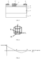
- a buffer layer 11, a gallium nitride layer 12 and an aluminum gallium nitride layer 13 are located on a substrate 10
- a gate electrode 14 a source electrode 15 and a drain electrode 16 are located on the aluminum gallium nitride layer 13.
- a portion of the aluminum gallium nitride layer below the gate electrode 4 is locally etched, so as to decrease a thickness of a portion of the aluminum gallium nitride layer in a gate region.
- Another way is to selectively remain p-type (A1)GaN below a gate electrode.
- the p-type (A1)GaN is used to increase conduction band energy level at an aluminum gallium nitride/gallium nitride heterojunction, so as to form a depletion region and thus implement an enhanced device.
- local p-type nitrides 17 are selectively remained below a gate electrode 14'.
- Still another way is to utilize fluoride plasma processing technology.
- Negatively charged ions such as fluorine ions are injected into a barrier layer. Concentration of injected ions can be controlled to deplete two-dimensional electron gas in a conduction channel, and strong negative ions are required to pinch off the channel. As shown in FIG. 3 , negatively charged ions 18 are injected into a barrier layer 13 below a gate electrode 14".
- a threshold voltage is generally about 0-1 V which is less than a threshold voltage of 3-5 V for an application.
- an additional dielectric layer such as aluminum oxide deposited in an atomic layer
- it is required to form an additional dielectric layer, such as aluminum oxide deposited in an atomic layer however, how to control an interface state between such a dielectric layer and an aluminum gallium nitride surface is a major problem unresolved.
- it is necessary to selectively etch away all areas except for those below the gate electrode how to precisely control an etching thickness is very challenging.
- defects caused by etching and magnesium atoms remaining in p-type aluminum gallium nitride will result in a severe current collapse effect.
- the present invention discloses a method for manufacturing an enhanced device.
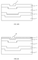
- the principle used to realize pinching off of the two-dimensional electron gas in the enhanced device is based on a characteristic of III group nitrides as a polar semiconductor.
- III group nitrides as a polar semiconductor.
- FIGS. 4 and 5 unlike traditional III-V group semiconductors, there are strong internal electric fields in the III group nitrides. If an AlInGaN/GaN heterojunction structure is formed at C(0002) plane, even without n-type doping in the AlInGaN layer, two-dimensional electron gas with very high concentration will be formed in the heterojunction. The reason lies in a spontaneous polarization electric field within the III group nitrides and a piezoelectric field caused by stresses.
- the concentration of the two-dimensional electron gas can be more than 1E13/cm 2 .
- the spontaneous polarization electric field and the piezoelectric field in the III group nitrides only exist in ⁇ 0002> direction, rather than the polarity direction, i.e., the direction perpendicular to the ⁇ 0002> direction.
- the polarity direction i.e., the direction perpendicular to the ⁇ 0002> direction.
- semi-polar directions for example, directions between the ⁇ 0002> and the ⁇ 1-100> or the ⁇ 11-20>, the intensities of the internal electric field in these directions are far less than those in the ⁇ 0002> direction.
- two-dimensional electron gas with very high concentration can be formed without intentional doping.
- the polarization field intensity is almost zero or very low
- two-dimensional electron gas will not be formed without doping.
- this invention by utilizing this feature of the gallium nitride material, grooves, protrusions or steps etc., are formed in a substrate and epitaxy parameters are controlled, so that the shape of the substrate is transferred to the channel layer, thus non-planar structures are formed in a gate region of the channel layer.
- two-dimensional electron gas is interrupted in the gate region, so that an enhanced device is implemented.
- Non-polar planes or semi-polar planes or combination thereof of nitrides formed in the non-planar structure will result in interruption of the two-dimensional electron gas, therefore, it is not necessary to etch the barrier layer, thereby avoiding performance deterioration due to damage to the active region, such as low current density or current collapse effect. Furthermore, it is no required to introduce Mg atoms to implement p-type nitrides, thereby avoiding contamination of the MOCVD or MBE chamber.
- a method of manufacturing an enhanced device comprising:
- step S1 further comprises:
- step S 1 further comprises:
- the non-planar structure includes a groove, a protrusion and a step.
- a cross-sectional shape of the groove is one of rectangle, triangle, trapezoid, zigzag, polygon, semicircle, U-shape or any combination thereof.
- a cross-sectional shape of the protrusion is one of rectangle, triangle, trapezoid, zigzag, polygon, semicircle, U-shape or any combination thereof.
- a cross-section of the step is a vertical surface, or a slope surface, or a curved surface, or an irregular surface.
- the step S1 further comprises: depositing a nitride nucleation layer on the substrate.
- the method further comprises depositing a dielectric layer on the nitride barrier layer.
- the dielectric layer includes any one of SiN, SiCN, SiO 2 , SiAlN, Al 2 O 3 , AlON, SiON, HfO 2 , HfAlO or any combination thereof.
- the method further comprises: depositing a nitride capping layer on the nitride barrier layer, the nitride capping layer includes gallium nitride or aluminum gallium nitride.
- the method further comprises: depositing an aluminum nitride intermediate layer on the nitride channel layer.
- the manufacturing method of an enhanced device according to the present invention it is not necessary to etch the nitride barrier layer, thereby avoiding performance deterioration due to damage to the active region, such as low current density or current collapse effect. Furthermore, it is no required to introduce Mg atoms to implement p-type nitrides, thereby avoiding contamination of the MOCVD or MBE chamber.
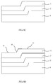
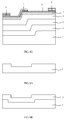
- FIGS. 6A-6G are schematic views illustrating a manufacturing process of an enhanced device according to a first embodiment of the present invention, wherein FIG. 6G is also a schematic view illustrating a structure of the enhanced device according to the first embodiment of the present invention.
- an enhanced device comprises:
- each of the substrate 1, the nitride nucleation layer 2, the nitride buffer layer 3, the nitride channel layer 4, the nitride barrier layer 5 and the dielectric layer 6 has a non-planar structure, and all of the non-planar structures are provided as rectangular grooves.
- a method of manufacturing an enhanced device comprises the flowing steps.
- the groove 41 is a rectangular groove.
- the groove 41 may have another shape, for example, a cross-sectional shape thereof may be one of triangle, trapezoid, zigzag, polygon, semicircle, U-shape or any combination thereof.
- the nitride nucleation layer 2, the nitride buffer layer 3 and the dielectric layer 6 are optional, and in other embodiments, all or part of them may be omitted.
- a nitride capping layer such as gallium nitride or aluminum gallium nitride may be grown on the nitride barrier layer; an aluminum nitride intermediate layer may be grown between the nitride barrier layer and the nitride channel layer.
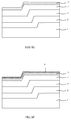
- FIGS. 7A-7G are schematic views illustrating a manufacturing process of an enhanced device according to a second embodiment of the present invention, wherein FIG. 7G is also a schematic view illustrating a structure of the enhanced device according to the second embodiment of the present invention.
- an enhanced device comprises:
- each of the substrate 1, the nitride nucleation layer 2, the nitride buffer layer 3, the nitride channel layer 4, the nitride barrier layer 5 and the dielectric layer 6 has a non-planar structure, and all of the non-planar structures are provided as rectangular protrusions.
- a method of manufacturing an enhanced device comprises the flowing steps.
- a source electrode 8 and a drain electrode 9 are formed in a source region and a drain region respectively, and form ohmic contacts with the nitride barrier layer 5 respectively.
- the protrusion 42 is a rectangular protrusion.
- the protrusion 42 may have another shape, for example, a cross-sectional shape thereof may be one of triangle, trapezoid, zigzag, polygon, semicircle, U-shape or any combination thereof.
- the nitride nucleation layer 2, the nitride buffer layer 3 and the dielectric layer 6 are optional, and in other embodiments, all or part of them may be omitted.
- a nitride capping layer such as gallium nitride or aluminum gallium nitride may be grown on the nitride barrier layer; an aluminum nitride intermediate layer may be grown between the nitride barrier layer and the nitride channel layer.
- FIGS. 8A-8G are schematic views illustrating a manufacturing process of an enhanced device according to a third embodiment of the present invention, wherein FIG. 8G is also a schematic view illustrating a structure of the enhanced device according to the third embodiment of the present invention.
- an enhanced device comprises:
- each of the substrate 1, the nitride nucleation layer 2, the nitride buffer layer 3, the nitride channel layer 4, the nitride barrier layer 5 and the dielectric layer 6 has a non-planar structure, and all of the non-planar structures are provided as steps.
- a method of manufacturing an enhanced device comprises the flowing steps.
- the connecting surfaces of the steps are slopes having certain angles.
- cross-sectional shapes of the steps may be other shapes, such as vertical surfaces, or curved surfaces, or irregular surfaces and so on.
- the nitride nucleation layer 2, the nitride buffer layer 3 and the dielectric layer 6 are optional, and in other embodiments, all or part of them may be omitted.
- a nitride capping layer such as gallium nitride or aluminum gallium nitride may be grown on the nitride barrier layer; an aluminum nitride intermediate layer may be grown between the nitride barrier layer and the nitride channel layer.
- FIGS. 9A-9G are schematic views illustrating a manufacturing process of an enhanced device according to a fourth embodiment of the present invention, wherein FIG. 9G is also a schematic view illustrating a structure of the enhanced device according to the fourth embodiment of the present invention.
- an enhanced device comprises:
- each of the substrate 1, the nitride nucleation layer 2, the nitride buffer layer 3, the nitride channel layer 4, the nitride barrier layer 5 and the dielectric layer 6 has a non-planar structure.
- the non-planar structures of the substrate 1, the nitride nucleation layer 2 and the nitride buffer layer 3 are provided as rectangular grooves, while the non-planar structures of the nitride channel 4, the nitride barrier layer 5 and the dielectric layer 6 are provided as triangular grooves.
- a method of manufacturing an enhanced device comprises the flowing steps.
- the groove 46 is a triangular groove.
- the groove 46 may have another shape, for example, a cross-sectional shape thereof may be one of rectangle, trapezoid, zigzag, polygon, semicircle, U-shape or any combination thereof.
- the nitride nucleation layer 2, the nitride buffer layer 3 and the dielectric layer 6 are optional, and in other embodiments, all or part of them may be omitted.
- a nitride capping layer such as gallium nitride or aluminum gallium nitride may be grown on the nitride barrier layer; an aluminum nitride intermediate layer may be grown between the nitride barrier layer and the nitride channel layer.
- FIG. 10 is a schematic view illustrating a structure of an enhanced device according to a fifth embodiment of the present invention.
- a groove of the substrate 1 has a rectangular shape
- grooves of a nitride nucleation layer 2 and a nitride buffer layer 3 have trapezoidal shapes
- grooves of a nitride channel layer 4, a nitride barrier layer 5 and a dielectric layer 6 have triangular shapes.
- Other aspects of this embodiment are the same as those of the first embodiment.
- FIG. 11 is a schematic view illustrating a structure of an enhanced device according to a sixth embodiment of the present invention.
- a groove of the substrate 1 has a trapezoidal shape
- grooves of a nitride nucleation layer 2, a nitride buffer layer 3, a nitride channel layer 4, a nitride barrier layer 5 and a dielectric layer 6 have trapezoidal shapes.
- Other aspects of this embodiment are the same as those of the first embodiment.
- the present invention provides a method for manufacturing an enhanced device. Since the shape of the substrate is transferred to the nitride channel layer during manufacturing process of the enhanced device, a non-planar structure is formed in a gate region of the nitride channel layer. Non-polar planes, or semi-polar planes or combination thereof of nitrides formed in the non-planar structure will result in interruption of the two-dimensional electron gas, therefore, it is not necessary to etch the nitride barrier layer, thereby avoiding performance deterioration due to damage to the active region, such as low current density or current collapse effect. Furthermore, it is no required to introduce Mg atoms to implement p-type nitrides, thereby avoiding contamination of the MOCVD or MBE chamber.
Landscapes
- Junction Field-Effect Transistors (AREA)
- Insulated Gate Type Field-Effect Transistor (AREA)
Applications Claiming Priority (2)
| Application Number | Priority Date | Filing Date | Title |
|---|---|---|---|
| CN201310738667.7A CN103715086A (zh) | 2013-12-27 | 2013-12-27 | 一种增强型器件的制造方法 |
| PCT/CN2014/094757 WO2015096723A1 (zh) | 2013-12-27 | 2014-12-24 | 一种增强型器件的制造方法 |
Publications (2)
| Publication Number | Publication Date |
|---|---|
| EP3089201A1 true EP3089201A1 (de) | 2016-11-02 |
| EP3089201A4 EP3089201A4 (de) | 2017-05-31 |
Family
ID=50407961
Family Applications (1)
| Application Number | Title | Priority Date | Filing Date |
|---|---|---|---|
| EP14874311.5A Withdrawn EP3089201A4 (de) | 2013-12-27 | 2014-12-24 | Verfahren zur herstellung einer verbesserten komponente |
Country Status (5)
| Country | Link |
|---|---|
| US (1) | US10026834B2 (de) |
| EP (1) | EP3089201A4 (de) |
| JP (1) | JP2017502519A (de) |
| CN (1) | CN103715086A (de) |
| WO (1) | WO2015096723A1 (de) |
Families Citing this family (21)
| Publication number | Priority date | Publication date | Assignee | Title |
|---|---|---|---|---|
| CN103715086A (zh) * | 2013-12-27 | 2014-04-09 | 苏州晶湛半导体有限公司 | 一种增强型器件的制造方法 |
| CN105702821B (zh) * | 2016-03-29 | 2018-01-30 | 苏州晶湛半导体有限公司 | 半导体发光器件及其制造方法 |
| JP6725455B2 (ja) * | 2017-06-22 | 2020-07-22 | 株式会社東芝 | 半導体装置及びその製造方法 |
| JP7203727B2 (ja) | 2017-07-07 | 2023-01-13 | パナソニックホールディングス株式会社 | 半導体装置 |
| JP6989660B2 (ja) * | 2017-09-19 | 2022-01-05 | 株式会社東芝 | 半導体装置及びその製造方法 |
| TWI646691B (zh) * | 2017-11-22 | 2019-01-01 | 友達光電股份有限公司 | 主動元件基板及其製造方法 |
| CN109935630B (zh) * | 2017-12-15 | 2021-04-23 | 苏州能讯高能半导体有限公司 | 半导体器件及其制造方法 |
| CN108461493A (zh) | 2018-01-05 | 2018-08-28 | 上海和辉光电有限公司 | 一种共栅晶体管、像素电路、像素结构及显示面板 |
| JP2019169572A (ja) * | 2018-03-22 | 2019-10-03 | 株式会社東芝 | 半導体装置及びその製造方法 |
| CN109742072B (zh) | 2019-01-04 | 2019-08-16 | 苏州汉骅半导体有限公司 | 集成增强型和耗尽型的hemt及其制造方法 |
| CN111863954B (zh) * | 2019-04-26 | 2026-01-02 | 苏州晶湛半导体有限公司 | 一种增强型器件及其制备方法 |
| CN110299408A (zh) * | 2019-07-22 | 2019-10-01 | 东南大学 | 一种具有槽栅调制结构的半极性GaN基增强型高电子迁移率晶体管 |
| JP7262379B2 (ja) * | 2019-12-16 | 2023-04-21 | 株式会社東芝 | 半導体装置 |
| CN213905363U (zh) * | 2020-12-17 | 2021-08-06 | 苏州晶湛半导体有限公司 | 一种增强型半导体器件 |
| CN113284949B (zh) * | 2021-07-20 | 2021-11-19 | 绍兴中芯集成电路制造股份有限公司 | 氮化镓基器件及其制造方法 |
| JP7534269B2 (ja) * | 2021-07-26 | 2024-08-14 | 株式会社東芝 | 半導体装置 |
| CN115810663B (zh) * | 2021-09-14 | 2026-04-03 | 联华电子股份有限公司 | 高电子迁移率晶体管及其制作方法 |
| US12218202B2 (en) * | 2021-09-16 | 2025-02-04 | Wolfspeed, Inc. | Semiconductor device incorporating a substrate recess |
| CN114975101B (zh) * | 2022-07-29 | 2022-11-15 | 江苏能华微电子科技发展有限公司 | 一种GaN器件及其制备方法 |
| CN116364774B (zh) * | 2023-03-15 | 2024-08-09 | 厦门市三安集成电路有限公司 | 一种高电子迁移率晶体管及其制作方法 |
| CN116314282A (zh) * | 2023-05-25 | 2023-06-23 | 北京大学 | 一种增强型氮化镓基电子器件及其制备方法 |
Family Cites Families (11)
| Publication number | Priority date | Publication date | Assignee | Title |
|---|---|---|---|---|
| JPH03290975A (ja) * | 1990-04-09 | 1991-12-20 | Fujitsu Ltd | 縦型半導体装置 |
| JP3546023B2 (ja) * | 2001-03-23 | 2004-07-21 | 三菱電線工業株式会社 | 結晶成長用基板の製造方法、およびGaN系結晶の製造方法 |
| US7052942B1 (en) * | 2003-09-19 | 2006-05-30 | Rf Micro Devices, Inc. | Surface passivation of GaN devices in epitaxial growth chamber |
| JP5261945B2 (ja) * | 2007-02-23 | 2013-08-14 | サンケン電気株式会社 | 電界効果半導体装置及びその製造方法 |
| JP5245305B2 (ja) * | 2007-07-06 | 2013-07-24 | サンケン電気株式会社 | 電界効果半導体装置及びその製造方法 |
| US7851825B2 (en) * | 2007-12-10 | 2010-12-14 | Transphorm Inc. | Insulated gate e-mode transistors |
| CN101252088B (zh) * | 2008-03-28 | 2010-04-14 | 西安电子科技大学 | 一种增强型A1GaN/GaN HEMT器件的实现方法 |
| CN102130160A (zh) * | 2011-01-06 | 2011-07-20 | 西安电子科技大学 | 槽形沟道AlGaN/GaN增强型HEMT器件及制作方法 |
| US8604486B2 (en) * | 2011-06-10 | 2013-12-10 | International Rectifier Corporation | Enhancement mode group III-V high electron mobility transistor (HEMT) and method for fabrication |
| CN102856370B (zh) * | 2012-09-18 | 2016-04-13 | 苏州晶湛半导体有限公司 | 一种增强型开关器件 |
| CN103715086A (zh) * | 2013-12-27 | 2014-04-09 | 苏州晶湛半导体有限公司 | 一种增强型器件的制造方法 |
-
2013
- 2013-12-27 CN CN201310738667.7A patent/CN103715086A/zh active Pending
-
2014
- 2014-12-24 WO PCT/CN2014/094757 patent/WO2015096723A1/zh not_active Ceased
- 2014-12-24 JP JP2016542926A patent/JP2017502519A/ja active Pending
- 2014-12-24 EP EP14874311.5A patent/EP3089201A4/de not_active Withdrawn
-
2016
- 2016-06-23 US US15/190,690 patent/US10026834B2/en active Active
Also Published As
| Publication number | Publication date |
|---|---|
| EP3089201A4 (de) | 2017-05-31 |
| JP2017502519A (ja) | 2017-01-19 |
| US20160300941A1 (en) | 2016-10-13 |
| WO2015096723A1 (zh) | 2015-07-02 |
| CN103715086A (zh) | 2014-04-09 |
| US10026834B2 (en) | 2018-07-17 |
Similar Documents
| Publication | Publication Date | Title |
|---|---|---|
| US10026834B2 (en) | Method of manufacturing enhanced device and enhanced device | |
| US12094962B2 (en) | Enhancement-mode semiconductor device and preparation method therefor | |
| Shibata et al. | 1.7 kV/1.0 mΩcm 2 normally-off vertical GaN transistor on GaN substrate with regrown p-GaN/AlGaN/GaN semipolar gate structure | |
| Lian et al. | AlGaN/GaN Schottky barrier diodes on silicon substrates with selective Si diffusion for low onset voltage and high reverse blocking | |
| CN105164811B (zh) | 半导体器件的电极及其形成方法 | |
| CN114899227B (zh) | 一种增强型氮化镓基晶体管及其制备方法 | |
| JP5190923B2 (ja) | GaNをチャネル層とする窒化物半導体トランジスタ及びその作製方法 | |
| EP2533292A2 (de) | Gruppe III-V Transistor mit hoher Elektronenbeweglichkeit (HEMT) vom Anreicherungstyp und Herstellungsverfahren | |
| JP5780613B2 (ja) | 改良された接着力を有する半導体デバイス及びその製造方法 | |
| TW202105524A (zh) | 氮化物半導體裝置及其製造方法 | |
| CN103594507B (zh) | 高击穿电压iii族氮化物器件 | |
| CN107851663A (zh) | 半导体器件和用于制造半导体器件的方法 | |
| JP2009141244A (ja) | 窒化物半導体トランジスタ及びその製造方法 | |
| US20180138305A1 (en) | Semiconductor device and method of manufacturing the same | |
| US20150123139A1 (en) | High electron mobility transistor and method of manufacturing the same | |
| TWI887332B (zh) | 基於iii族氮化物半導體之異質接面裝置以及製造一基於iii族氮化物半導體之異質接面裝置之方法 | |
| CN102856370B (zh) | 一种增强型开关器件 | |
| CN102856355A (zh) | 增强型半导体器件 | |
| CN102856366A (zh) | 一种增强型器件 | |
| CN107958939A (zh) | 一种氮化鎵基异质结肖特基二极管结构 | |
| US12002879B2 (en) | High electron mobility transistor and method of manufacturing the same | |
| EP3405979B1 (de) | Halbleiterbauelement, elektronisches teil, elektronische vorrichtung und verfahren zur herstellung eines halbleiterbauelements | |
| CN210897283U (zh) | 一种半导体器件 | |
| CN106531789A (zh) | 通过极性控制实现增强型hemt的方法及增强型hemt | |
| US20150187925A1 (en) | Enhancement-mode device |
Legal Events
| Date | Code | Title | Description |
|---|---|---|---|
| PUAI | Public reference made under article 153(3) epc to a published international application that has entered the european phase |
Free format text: ORIGINAL CODE: 0009012 |
|
| 17P | Request for examination filed |
Effective date: 20160727 |
|
| AK | Designated contracting states |
Kind code of ref document: A1 Designated state(s): AL AT BE BG CH CY CZ DE DK EE ES FI FR GB GR HR HU IE IS IT LI LT LU LV MC MK MT NL NO PL PT RO RS SE SI SK SM TR |
|
| AX | Request for extension of the european patent |
Extension state: BA ME |
|
| DAX | Request for extension of the european patent (deleted) | ||
| RIN1 | Information on inventor provided before grant (corrected) |
Inventor name: CHENG, KAI |
|
| A4 | Supplementary search report drawn up and despatched |
Effective date: 20170503 |
|
| RIC1 | Information provided on ipc code assigned before grant |
Ipc: H01L 29/10 20060101ALI20170425BHEP Ipc: H01L 21/338 20060101ALI20170425BHEP Ipc: H01L 29/423 20060101ALI20170425BHEP Ipc: H01L 29/20 20060101ALN20170425BHEP Ipc: H01L 29/778 20060101AFI20170425BHEP |
|
| STAA | Information on the status of an ep patent application or granted ep patent |
Free format text: STATUS: THE APPLICATION IS DEEMED TO BE WITHDRAWN |
|
| 18D | Application deemed to be withdrawn |
Effective date: 20171130 |