EP3405979B1 - Halbleiterbauelement, elektronisches teil, elektronische vorrichtung und verfahren zur herstellung eines halbleiterbauelements - Google Patents
Halbleiterbauelement, elektronisches teil, elektronische vorrichtung und verfahren zur herstellung eines halbleiterbauelements Download PDFInfo
- Publication number
- EP3405979B1 EP3405979B1 EP17702170.6A EP17702170A EP3405979B1 EP 3405979 B1 EP3405979 B1 EP 3405979B1 EP 17702170 A EP17702170 A EP 17702170A EP 3405979 B1 EP3405979 B1 EP 3405979B1
- Authority
- EP
- European Patent Office
- Prior art keywords
- layer
- semiconductor device
- electrode
- channel
- contact layer
- Prior art date
- Legal status (The legal status is an assumption and is not a legal conclusion. Google has not performed a legal analysis and makes no representation as to the accuracy of the status listed.)
- Active
Links
Images







Classifications
-
- H—ELECTRICITY
- H10—SEMICONDUCTOR DEVICES; ELECTRIC SOLID-STATE DEVICES NOT OTHERWISE PROVIDED FOR
- H10D—INORGANIC ELECTRIC SEMICONDUCTOR DEVICES
- H10D30/00—Field-effect transistors [FET]
- H10D30/40—FETs having zero-dimensional [0D], one-dimensional [1D] or two-dimensional [2D] charge carrier gas channels
- H10D30/47—FETs having zero-dimensional [0D], one-dimensional [1D] or two-dimensional [2D] charge carrier gas channels having two-dimensional [2D] charge carrier gas channels, e.g. nanoribbon FETs or high electron mobility transistors [HEMT]
- H10D30/471—High electron mobility transistors [HEMT] or high hole mobility transistors [HHMT]
- H10D30/477—Vertical HEMTs or vertical HHMTs
-
- H—ELECTRICITY
- H10—SEMICONDUCTOR DEVICES; ELECTRIC SOLID-STATE DEVICES NOT OTHERWISE PROVIDED FOR
- H10D—INORGANIC ELECTRIC SEMICONDUCTOR DEVICES
- H10D30/00—Field-effect transistors [FET]
- H10D30/01—Manufacture or treatment
- H10D30/015—Manufacture or treatment of FETs having heterojunction interface channels or heterojunction gate electrodes, e.g. HEMT
-
- H—ELECTRICITY
- H10—SEMICONDUCTOR DEVICES; ELECTRIC SOLID-STATE DEVICES NOT OTHERWISE PROVIDED FOR
- H10D—INORGANIC ELECTRIC SEMICONDUCTOR DEVICES
- H10D30/00—Field-effect transistors [FET]
- H10D30/40—FETs having zero-dimensional [0D], one-dimensional [1D] or two-dimensional [2D] charge carrier gas channels
- H10D30/47—FETs having zero-dimensional [0D], one-dimensional [1D] or two-dimensional [2D] charge carrier gas channels having two-dimensional [2D] charge carrier gas channels, e.g. nanoribbon FETs or high electron mobility transistors [HEMT]
- H10D30/471—High electron mobility transistors [HEMT] or high hole mobility transistors [HHMT]
- H10D30/473—High electron mobility transistors [HEMT] or high hole mobility transistors [HHMT] having confinement of carriers by multiple heterojunctions, e.g. quantum well HEMT
- H10D30/4732—High electron mobility transistors [HEMT] or high hole mobility transistors [HHMT] having confinement of carriers by multiple heterojunctions, e.g. quantum well HEMT using Group III-V semiconductor material
-
- H—ELECTRICITY
- H10—SEMICONDUCTOR DEVICES; ELECTRIC SOLID-STATE DEVICES NOT OTHERWISE PROVIDED FOR
- H10D—INORGANIC ELECTRIC SEMICONDUCTOR DEVICES
- H10D30/00—Field-effect transistors [FET]
- H10D30/40—FETs having zero-dimensional [0D], one-dimensional [1D] or two-dimensional [2D] charge carrier gas channels
- H10D30/47—FETs having zero-dimensional [0D], one-dimensional [1D] or two-dimensional [2D] charge carrier gas channels having two-dimensional [2D] charge carrier gas channels, e.g. nanoribbon FETs or high electron mobility transistors [HEMT]
- H10D30/471—High electron mobility transistors [HEMT] or high hole mobility transistors [HHMT]
- H10D30/478—High electron mobility transistors [HEMT] or high hole mobility transistors [HHMT] the 2D charge carrier gas being at least partially not parallel to a main surface of the semiconductor body
-
- H—ELECTRICITY
- H10—SEMICONDUCTOR DEVICES; ELECTRIC SOLID-STATE DEVICES NOT OTHERWISE PROVIDED FOR
- H10D—INORGANIC ELECTRIC SEMICONDUCTOR DEVICES
- H10D30/00—Field-effect transistors [FET]
- H10D30/60—Insulated-gate field-effect transistors [IGFET]
- H10D30/63—Vertical IGFETs
-
- H—ELECTRICITY
- H10—SEMICONDUCTOR DEVICES; ELECTRIC SOLID-STATE DEVICES NOT OTHERWISE PROVIDED FOR
- H10D—INORGANIC ELECTRIC SEMICONDUCTOR DEVICES
- H10D30/00—Field-effect transistors [FET]
- H10D30/80—FETs having rectifying junction gate electrodes
- H10D30/801—FETs having heterojunction gate electrodes
-
- H—ELECTRICITY
- H10—SEMICONDUCTOR DEVICES; ELECTRIC SOLID-STATE DEVICES NOT OTHERWISE PROVIDED FOR
- H10D—INORGANIC ELECTRIC SEMICONDUCTOR DEVICES
- H10D62/00—Semiconductor bodies, or regions thereof, of devices having potential barriers
- H10D62/10—Shapes, relative sizes or dispositions of the regions of the semiconductor bodies; Shapes of the semiconductor bodies
- H10D62/117—Shapes of semiconductor bodies
-
- H—ELECTRICITY
- H10—SEMICONDUCTOR DEVICES; ELECTRIC SOLID-STATE DEVICES NOT OTHERWISE PROVIDED FOR
- H10D—INORGANIC ELECTRIC SEMICONDUCTOR DEVICES
- H10D62/00—Semiconductor bodies, or regions thereof, of devices having potential barriers
- H10D62/10—Shapes, relative sizes or dispositions of the regions of the semiconductor bodies; Shapes of the semiconductor bodies
- H10D62/13—Semiconductor regions connected to electrodes carrying current to be rectified, amplified or switched, e.g. source or drain regions
- H10D62/149—Source or drain regions of field-effect devices
-
- H—ELECTRICITY
- H10—SEMICONDUCTOR DEVICES; ELECTRIC SOLID-STATE DEVICES NOT OTHERWISE PROVIDED FOR
- H10D—INORGANIC ELECTRIC SEMICONDUCTOR DEVICES
- H10D64/00—Electrodes of devices having potential barriers
- H10D64/20—Electrodes characterised by their shapes, relative sizes or dispositions
- H10D64/27—Electrodes not carrying the current to be rectified, amplified, oscillated or switched, e.g. gates
- H10D64/311—Gate electrodes for field-effect devices
- H10D64/411—Gate electrodes for field-effect devices for FETs
- H10D64/511—Gate electrodes for field-effect devices for FETs for IGFETs
- H10D64/512—Disposition of the gate electrodes, e.g. buried gates
-
- H—ELECTRICITY
- H10—SEMICONDUCTOR DEVICES; ELECTRIC SOLID-STATE DEVICES NOT OTHERWISE PROVIDED FOR
- H10D—INORGANIC ELECTRIC SEMICONDUCTOR DEVICES
- H10D64/00—Electrodes of devices having potential barriers
- H10D64/20—Electrodes characterised by their shapes, relative sizes or dispositions
- H10D64/27—Electrodes not carrying the current to be rectified, amplified, oscillated or switched, e.g. gates
- H10D64/311—Gate electrodes for field-effect devices
- H10D64/411—Gate electrodes for field-effect devices for FETs
- H10D64/511—Gate electrodes for field-effect devices for FETs for IGFETs
- H10D64/517—Gate electrodes for field-effect devices for FETs for IGFETs characterised by the conducting layers
- H10D64/519—Gate electrodes for field-effect devices for FETs for IGFETs characterised by the conducting layers characterised by their top-view geometrical layouts
-
- H—ELECTRICITY
- H10—SEMICONDUCTOR DEVICES; ELECTRIC SOLID-STATE DEVICES NOT OTHERWISE PROVIDED FOR
- H10P—GENERIC PROCESSES OR APPARATUS FOR THE MANUFACTURE OR TREATMENT OF DEVICES COVERED BY CLASS H10
- H10P50/00—Etching of wafers, substrates or parts of devices
- H10P50/20—Dry etching; Plasma etching; Reactive-ion etching
- H10P50/26—Dry etching; Plasma etching; Reactive-ion etching of conductive or resistive materials
- H10P50/264—Dry etching; Plasma etching; Reactive-ion etching of conductive or resistive materials by chemical means
- H10P50/266—Dry etching; Plasma etching; Reactive-ion etching of conductive or resistive materials by chemical means by vapour etching only
-
- H—ELECTRICITY
- H10—SEMICONDUCTOR DEVICES; ELECTRIC SOLID-STATE DEVICES NOT OTHERWISE PROVIDED FOR
- H10D—INORGANIC ELECTRIC SEMICONDUCTOR DEVICES
- H10D30/00—Field-effect transistors [FET]
- H10D30/01—Manufacture or treatment
- H10D30/021—Manufacture or treatment of FETs having insulated gates [IGFET]
- H10D30/025—Manufacture or treatment of FETs having insulated gates [IGFET] of vertical IGFETs
-
- H—ELECTRICITY
- H10—SEMICONDUCTOR DEVICES; ELECTRIC SOLID-STATE DEVICES NOT OTHERWISE PROVIDED FOR
- H10D—INORGANIC ELECTRIC SEMICONDUCTOR DEVICES
- H10D62/00—Semiconductor bodies, or regions thereof, of devices having potential barriers
- H10D62/10—Shapes, relative sizes or dispositions of the regions of the semiconductor bodies; Shapes of the semiconductor bodies
- H10D62/113—Isolations within a component, i.e. internal isolations
- H10D62/115—Dielectric isolations, e.g. air gaps
-
- H—ELECTRICITY
- H10—SEMICONDUCTOR DEVICES; ELECTRIC SOLID-STATE DEVICES NOT OTHERWISE PROVIDED FOR
- H10D—INORGANIC ELECTRIC SEMICONDUCTOR DEVICES
- H10D62/00—Semiconductor bodies, or regions thereof, of devices having potential barriers
- H10D62/10—Shapes, relative sizes or dispositions of the regions of the semiconductor bodies; Shapes of the semiconductor bodies
- H10D62/17—Semiconductor regions connected to electrodes not carrying current to be rectified, amplified or switched, e.g. channel regions
- H10D62/351—Substrate regions of field-effect devices
- H10D62/357—Substrate regions of field-effect devices of FETs
-
- H—ELECTRICITY
- H10—SEMICONDUCTOR DEVICES; ELECTRIC SOLID-STATE DEVICES NOT OTHERWISE PROVIDED FOR
- H10D—INORGANIC ELECTRIC SEMICONDUCTOR DEVICES
- H10D62/00—Semiconductor bodies, or regions thereof, of devices having potential barriers
- H10D62/80—Semiconductor bodies, or regions thereof, of devices having potential barriers characterised by the materials
- H10D62/85—Semiconductor bodies, or regions thereof, of devices having potential barriers characterised by the materials being Group III-V materials, e.g. GaAs
- H10D62/8503—Nitride Group III-V materials, e.g. AlN or GaN
-
- H—ELECTRICITY
- H10—SEMICONDUCTOR DEVICES; ELECTRIC SOLID-STATE DEVICES NOT OTHERWISE PROVIDED FOR
- H10D—INORGANIC ELECTRIC SEMICONDUCTOR DEVICES
- H10D64/00—Electrodes of devices having potential barriers
- H10D64/20—Electrodes characterised by their shapes, relative sizes or dispositions
- H10D64/23—Electrodes carrying the current to be rectified, amplified, oscillated or switched, e.g. sources, drains, anodes or cathodes
- H10D64/251—Source or drain electrodes for field-effect devices
- H10D64/257—Source or drain electrodes for field-effect devices for lateral devices wherein the source or drain electrodes are characterised by top-view geometrical layouts, e.g. interdigitated, semi-circular, annular or L-shaped electrodes
Definitions
- the present disclosure relates to semiconductor devices, electronic parts, electronic apparatuses, and methods for fabricating a semiconductor device.
- HEMT high electron mobility transistor
- the high electron mobility transistor is a field effect transistor in which a two-dimensional electron gas layer formed by a heterojunction of compound semiconductors is used as a channel.
- the two-dimensional electron gas layer has a high electron mobility and a high sheet electron density. Therefore, the high electron mobility transistor is a semiconductor device which can perform a low-resistance, high-speed, and high-breakdown-voltage operation.
- a high electron mobility transistor has a structure in which a barrier layer is provided on a channel layer, and a source electrode and a drain electrode are provided on the barrier layer.
- the barrier layer having a wide band gap serves as a potential barrier, and therefore, the contact resistances between the source and drain electrodes, and the two-dimensional electron gas layer, which is a channel, are high.
- Patent application JP 2008 218846 (A ) describes a nitride semiconductor element capable of improving a breakdown voltage between a gate and a drain.
- Japanese patent application JPH0715018 describes a HEMT with a substrate; a first contact layer on the substrate; a channel layer on the first contact layer, the channel layer including a two-dimensional electron gas layer on side-wall surfaces of the channel layer in a direction perpendicular to the substrate; a second contact layer on the channel layer; a barrier layer on the first contact layer, and on the side walls of the channel layer; a gate electrode on at least one side surface of the barrier layer; a first electrode on the first contact layer; a second electrode on the second contact layer, wherein the first contact layer and the second contact layer are of a first conductivity type.
- the invention provides a semiconductor device in accordance with independent claim 1.
- the invention provides an electronic part in accordance with dependent claim 8.
- the invention provides an electronic apparatus in accordance with dependent claim 9.
- the invention provides a method for fabricating an electronic device in accordance with independent claim 10.
- the distance between the source electrode and the drain electrode can be reduced without using state-of-the-art fabrication equipment.
- the on-resistance of a semiconductor device can be further reduced.
- FIG. 17 is a cross-sectional view showing a multilayer structure of a compound semiconductor transistor which is a semiconductor device according to a comparative example.
- the compound semiconductor transistor 10 according to the comparative example includes a buffer layer 51 provided on a substrate 50, a channel layer 30 provided on the buffer layer 51, a barrier layer 31 provided on the channel layer 30, a gate electrode 40, source electrode 21, and drain electrode 11 provided on the barrier layer 31, and an insulating layer 52 which insulates the gate electrode 40, the source electrode 21, and the drain electrode 11 from each other. Also, a two-dimensional electron gas layer 32 which is a channel is formed in the vicinity of an interface of the channel layer 30 which is in contact with the barrier layer 31.
- the substrate 50 is formed of, for example, silicon (Si), silicon carbide (SiC), gallium nitride (GaN), sapphire, or the like.
- the buffer layer 51 is formed of a compound semiconductor material, and is for epitaxially growing the channel layer 30 and the barrier layer 31 on the substrate 50.
- the buffer layer 51 is formed of a compound semiconductor material the grating constant of which is appropriately controlled, and can be used to control the crystal orientation and crystalline state of the channel layer 30 provided on the buffer layer 51. As a result, even when the substrate 50 and the channel layer 30 have significantly different grating constants, the channel layer 30 can be epitaxially grown.
- the channel layer 30 is formed of a compound semiconductor material
- the barrier layer 31 is formed of a compound semiconductor material different from that of the channel layer 30.
- the different compound semiconductor materials are joined together at an interface between the channel layer 30 and the barrier layer 31, so that an electron layer called the two-dimensional electron gas layer 32 is formed.
- the channel layer 30 in which the two-dimensional electron gas layer 32 is formed may be formed of an i-type (i.e., undoped) compound semiconductor.
- the barrier layer 31 may be formed of either an i-type or n-type compound semiconductor if the barrier layer 31 allows formation of the two-dimensional electron gas layer 32.
- the barrier layer 31 may be formed of an n-type compound semiconductor in order to increase the electron density of the two-dimensional electron gas layer 32 which is a channel.
- a compound semiconductor transistor which includes such a two-dimensional electron gas layer (32) as a channel is also called a “high electron mobility transistor (HEMT). "
- Examples of the combination of compound semiconductor materials which form such a heterojunction include GaAs and AlGaAs, GaN and AlGaN, GaAs and InGaP, GaN and AlInN, and the like.
- the gate electrode 40 is formed of a metal such as nickel (Ni), titanium (Ti), gold (Au), or the like.
- the gate electrode 40 and the barrier layer 31 form a Schottky junction, which forms, in the barrier layer 31, a depletion layer extending from the gate electrode 40.
- the two-dimensional electron gas layer 32 formed in the channel layer 30 forms a depletion layer extending from the channel layer 30.
- the electron concentration of the two-dimensional electron gas layer 32 can be controlled by controlling a voltage applied to the gate electrode 40 so that the compound semiconductor transistor 10 functions as an field effect transistor in which a two-dimensional electron gas layer is a channel.
- the source electrode 21 and the drain electrode 11 are formed of a metal such as titanium (Ti), aluminum (Al), or the like. Also, the source electrode 21 and the drain electrode 11 are formed to provide an ohmic contact with the channel layer 30.
- the resistance during operation (also called an "on-resistance") is high.
- the barrier layer 31, which is a high potential barrier is interposed between each of the source electrode 21 and the drain electrode 11, and the two-dimensional electron gas layer 32 which is a channel, so that the contact resistance is high.
- a technique of reducing the potential barrier by replacing a portion of the barrier layer 31 with a layer doped with impurities at a high concentration has been proposed.
- a technique of alloying a metal of which the source electrode 21 and the drain electrode 11 are formed, and the barrier layer 31, by high-temperature annealing has been proposed.
- the contact resistance is only reduced, there is a limit on the decrease of the on-resistance of the compound semiconductor transistor 10. This is because the on-resistance of the compound semiconductor transistor 10 includes a channel resistance depending on the distance between the source electrode 21 and the drain electrode 11.
- the channel resistance may be reduced by, for example, employing a fabrication process capable of further miniaturization and thereby reducing the distance between the source electrode 21 and the drain electrode 11.
- a fabrication process capable of further miniaturization is employed, the fabrication cost increases significantly. Therefore, it has been difficult to further reduce the on-resistance of the compound semiconductor transistor 10 while inhibiting the increase of the fabrication cost.
- a semiconductor device has a novel and improved structure in which the distance between the source electrode and the drain electrode can be reduced so that the on-resistance is further reduced.
- FIG. 1 is a cross-sectional view showing the multilayer structure of the semiconductor device 1 according to this embodiment.
- the semiconductor device 1 includes a substrate 500, a buffer layer 510, a first contact layer 100, a channel layer (or region) 300, a second contact layer 200, a barrier layer 310, a gate electrode 400, a first electrode 110, a second electrode 210, and an insulating layer 520.
- the semiconductor device 1 is a high electron mobility transistor.
- a two-dimensional electron gas layer 320 which is a channel is formed in the vicinity of an interface of the channel layer 300 which is in contact with the barrier layer 310, substantially perpendicularly to the substrate 500.
- the substrate 500 is formed of a compound semiconductor material.
- the substrate 500 is formed of a group III-V compound semiconductor material.
- the substrate 500 may be a semi-insulating monocrystalline gallium nitride (GaN) substrate.
- the buffer layer 510 described below the substrate 500 may be formed of a material which has a grating constant different from that of the first contact layer 100 provided on the substrate 500.
- the substrate 500 may, for example, be a silicon (Si) substrate, silicon carbide (SiC) substrate, sapphire substrate, or the like.
- the buffer layer 510 is provided on the substrate 500, and is formed of an epitaxially grown compound semiconductor material. Specifically, the buffer layer 510 is formed of a compound semiconductor material having an appropriate grating constant based on the grating constants of the substrate 500 and the first contact layer 100. When the substrate 500 and the first contact layer 100 have different grating constants, the grating constant of the buffer layer 510 can be controlled so that the first contact layer 100 can have a good crystalline state and the warpage of the semiconductor device 1 is controlled. For example, when the substrate 500 is a Si substrate, and the first contact layer 100 is formed of GaN, the buffer layer 510 can be formed of AlN, AlGaN, GaN, or the like.
- the first contact layer 100 is provided on the buffer layer 510, and is formed of a compound semiconductor material doped with an impurity at a high concentration.
- the first contact layer 100 may be formed of the same compound semiconductor material as that of the channel layer 300 described below that is doped with an n-type impurity at a high concentration.
- the first contact layer 100 the resistance of which is reduced by the high-concentration doping, can reduce the contact resistance between the first contact layer 100 and the first electrode 110.
- the first contact layer 100 may be formed of epitaxially grown GaN which is doped with silicon (Si) or germanium (Ge).
- the concentration of the impurity for the doping may be 1.0 ⁇ 10 18 /cm 3 or more.
- the channel layer 300 is provided in an island shape on a partial region of the first contact layer 100, and is formed of a compound semiconductor material in which carriers are accumulated due to a heterojunction between the channel layer 300 and the barrier layer 310.
- the two-dimensional electron gas layer 320 is formed on a side surface of the channel layer 300, in a direction substantially perpendicular to the substrate 500.
- the channel layer 300 may be formed of a compound semiconductor material which is not doped with an impurity, i.e., an i-type (i.e., undoped) compound semiconductor material. In such a case, in the channel layer 300, carrier scattering caused by impurities is inhibited, and therefore, carrier mobility can be improved in the two-dimensional electron gas layer 320.
- the channel layer 300 may be formed of epitaxially grown GaN.
- the two-dimensional electron gas layer 320 is epitaxially grown and formed on the side surface of the channel layer 300 so that the C-axis direction of the crystal is substantially perpendicular to the side surface of the channel layer 300.
- a two-dimensional electron gas layer is formed on the polar c-plane (0001) of the crystal. Therefore, the crystal orientation of the channel layer 300 may be appropriately controlled so that the two-dimensional electron gas layer 320 is formed on the side surface of the channel layer 300.
- the C-axis of the crystal orientation of the channel layer 300 may not be perpendicular to the side surface, and may be inclined in any direction by up to about 55°. Note that when the angle of the inclination is large, it is difficult to form the two-dimensional electron gas layer 320 on the side surface, and therefore, the inclination angle of the C-axis of the crystal may be within 10° or less in any direction with respect to the normal direction of the side surface.
- the second contact layer 200 is provided on the channel layer 300, and is formed of a compound semiconductor material doped with an impurity at a high concentration.
- the second contact layer 200 may be formed of the same compound semiconductor material as that of the channel layer 300 that is doped with an n-type impurity at a high concentration.
- the second contact layer 200 the resistance of which is reduced by the high-concentration doping, can reduce the contact resistance between the second contact layer 200 and the second electrode 210.
- the second contact layer 200 may be formed of epitaxially grown GaN which is doped with silicon (Si) or germanium (Ge).
- the concentration of the impurity for the doping may be 1.0 ⁇ 10 18 /cm 3 or more.
- the barrier layer 310 is provided on the first contact layer 100 and the second contact layer 200, and is formed of a compound semiconductor material which causes carriers to be accumulated in the channel layer 300 due to a heterojunction between the barrier layer 310 and the channel layer 300.
- the barrier layer 310 is formed of a compound semiconductor material different from that of the channel layer 300.
- the barrier layer 310 may be formed of a compound semiconductor material which is not doped with an impurity, i.e., an i-type (i.e., undoped) compound semiconductor material. In such a case, the barrier layer 310 can inhibit carrier scattering caused by impurities in the channel layer 300, and therefore, the carrier mobility of the two-dimensional electron gas layer 320 can be improved.
- the channel layer 300 and the barrier layer 310 may be formed of respective compound semiconductor materials a combination of which is different from that described above.
- the channel layer 300 and the barrier layer 310 may be formed of GaAs and AlGaAs, GaAs and InGaP, or GaN and AlInN, respectively.
- the gate electrode 400 is provided on the side surface of the channel layer 300 with the barrier layer 310 being interposed therebetween. Also, the gate electrode 400 is formed of a metal which forms a Schottky junction between the gate electrode 400 and the barrier layer 310. For example, the gate electrode 400 may be formed by successively forming a layer of nickel (Ni) and a layer of gold (Au) on top of each other, where the nickel layer is closer to the barrier layer 310. As a result, the concentration of the two-dimensional electron gas layer 320 can be controlled by controlling a voltage applied to the gate electrode 400.
- Ni nickel
- Au gold
- the gate electrode 400 is coupled to a control electrode 401 provided on the insulating layer 520, in a region outside a device region 600 where the semiconductor device 1 is provided. A voltage applied to the gate electrode 400 is controlled through the control electrode 401.
- the insulating layer 520 is formed of an insulating material, and is provided to cover the entire surfaces of the barrier layer 310 and the gate electrode 400.
- the insulating layer 520 insulates the barrier layer 310 and the gate electrode 400 from other electrodes, interconnects, and the like, and protects the barrier layer 310 and the gate electrode 400 from impurities such as ions and the like.
- the insulating layer 520 may be a monolayer film of, for example, SiN, Si 3 N 4 , SiO, SiO 2 , Al 2 O 3 , or the like, or a multilayer film thereof.
- the first electrode 110 is configured to be coupled to the first contact layer 100, while the second electrode 210 is configured to be coupled to the second contact layer 200.
- the first electrode 110 and the second electrode 210 may be formed by successively forming a layer of titanium (Ti) and a layer of aluminum (Al), or the like, on top of each other, where the titanium layer is closer to the first contact layer 100 and the second contact layer 200.
- the first electrode 110 may be a source electrode
- the second electrode 210 may be drain electrode, or vice versa, of course.
- the two-dimensional electron gas layer 320 is formed in the channel layer 300 by a heterojunction between the channel layer 300 and the barrier layer 310, substantially perpendicularly to the substrate 500.
- An upper end of the two-dimensional electron gas layer 320 is coupled to the second electrode 210 with the second contact layer 200 being interposed therebetween, while a lower end of the two-dimensional electron gas layer 320 is coupled to the first electrode 110 with the first contact layer 100 being interposed therebetween.
- the two-dimensional electron gas layer 320 forms a current path between the first electrode 110 and the second electrode 210.
- a current flowing between the first electrode 110 and the second electrode 210 can be modulated by the concentration of the two-dimensional electron gas layer 320 being modulated by a Schottky junction formed between the barrier layer 310 and the gate electrode 400.
- a positive bias is applied to the gate electrode 400
- a current flowing between the first electrode 110 and the second electrode 210 is generated by electrons accumulated in the two-dimensional electron gas layer 320.
- a negative bias is applied to the gate electrode 400, the Schottky junction depletes electrons in the two-dimensional electron gas layer 320 of the channel layer 300 facing the gate electrode 400, so that a current does not flow between the first electrode 110 and the second electrode 210.
- the gate electrode 400 and the second electrode 210 are between first and second portions of the first electrode 110 (e.g., where the first portion of the first electrode 110 is on a left side of the semiconductor device 1 and the second portion of the first electrode 110 is on a right side of the semiconductor device 1).
- the barrier layer 310 includes at least one side surface.
- the barrier layer 310 includes a first side surface and a second side surface (e.g., the surfaces adjacent to the two-dimensional electron gas layer 320).
- the gate electrode 400 includes a first portion on the first side surface of the barrier layer 310 and a second portion on the second side surface of the barrier layer 310 (e.g., where the first portion of the gate electrode 400 is on a left side of the semiconductor device 1 and the second portion of the gate electrode 400 is on a right side of the semiconductor device 1).
- the second electrode 210 is between the first and second portions of the gate electrode 400.
- the barrier layer 310 is on at least one side surface of the channel layer 300.
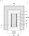
- FIG. 2 is a plan view showing the planar structure of the semiconductor device 1 according to this embodiment. Note that a cross-sectional structure of the semiconductor device 1 shown in FIG. 1 corresponds to a cross-sectional multilayer structure taken along a cut line A of FIG. 2 .
- the channel layer 300 is provided in an island shape in planar view, while the second contact layer 200 and the second electrode 210 are provided on the channel layer 300. Also, the barrier layer 310, the gate electrode 400, and the first electrode 110 are provided around the channel layer 300.
- the channel layer 300 is said to have an island shape because the first electrode 110 is disposed around at least three sides of the channel layer 300 in a plan view, and the gate electrode 400 and the barrier layer 310 surround the channel layer 300 in the plan view.
- example embodiments are not limited thereto.
- the first electrode 110 may be disposed around all sides of (i.e., surround) the channel layer 300, and the barrier layer 310 and the gate electrode 400 may be disposed around less than all four sides of the channel layer 300 (e.g., three sides).
- the barrier layer 310 is formed around the channel layer 300 and that the gate electrode 400 is formed around side surfaces of the barrier layer 310.
- each component of the semiconductor device 1 is provided in the device region 600.
- a region outside the device region 600 has a high resistance so that the semiconductor device 1 is electrically separated from other semiconductor devices provided on the substrate 500.
- the high resistance may be imparted to the region outside the device region 600 by, for example, injecting impurity ions such as boron (B) ions or the like into the first contact layer 100, or by burying an insulating material in an opening formed by removal of the first contact layer 100 using etching or the like.
- the control electrode 401 which is coupled to the gate electrode 400 and is used to control a voltage applied to the gate electrode 400, is provided in the region outside the device region 600.
- the two-dimensional electron gas layer 320 can be formed on the side surface of the channel layer 300 (specifically, a surface substantially perpendicular to the C-axis of the crystal), and therefore, the current density can be higher than that of the compound semiconductor transistor 10 shown in FIG. 17 .
- the thickness of the channel layer 300 corresponds to a distance between the source electrode and the drain electrode.
- the thickness of the channel layer 300 can be controlled on the nanometer scale without using state-of-the-art fabrication equipment, and therefore, in the semiconductor device 1, the distance between the source electrode and the drain electrode can be reduced irrespective of the miniaturization capability of the fabrication process. Therefore, in the semiconductor device 1 according to this embodiment, the reduction of the distance between the source electrode and the drain electrode can reduce the channel resistance, resulting in a reduction in the on-resistance.
- the thickness of the channel layer 300 also corresponds to the gate length. Therefore, the gate length can be similarly reduced irrespective of the miniaturization capability of the fabrication process, whereby the semiconductor device 1 can operate at higher speed.
- the side surface of the channel layer 300 formed in an island shape can be used as a channel to provide a higher current density, and therefore, the semiconductor device can have a size smaller than those of field effect transistors having other structures (e.g., the compound semiconductor transistor 10 shown in FIG. 17 ).
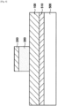
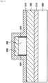
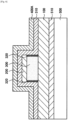
- FIG. 3 to FIG. 9 are cross-sectional views showing a process of fabricating the semiconductor device 1 shown in FIG. 1 .
- the buffer layer 510, the first contact layer 100, the channel layer 300, and the second contact layer 200 are epitaxially grown on top of each other, in that order, by metal organic chemical vapor deposition (MOCVD), molecular beam epitaxy (MBE), or the like.
- MOCVD metal organic chemical vapor deposition
- MBE molecular beam epitaxy
- the substrate 500 may be a silicon (Si) substrate.
- the buffer layer 510 is formed of, for example, AlN, AlGaN, or GaN, while the first contact layer 100 and the second contact layer 200 may be formed of, for example, n-type GaN doped with silicon (Si).
- the channel layer 300 may be formed of, for example, undoped GaN so that the C-axis of the crystal faces in a direction substantially perpendicular to the thickness direction of the substrate 500.
- the plane orientation of a surface of the substrate 500 on which the semiconductor device 1 is to be formed may be appropriately controlled.
- patterning is performed on the channel layer 300 and the second contact layer 200 by wet etching or dry etching using a photoresist as a mask. Note that when the first contact layer 100 and the channel layer 300 are formed of substantially the same compound semiconductor, a surface of the first contact layer 100 may be etched during this patterning step, which does not significantly affect the characteristics of the semiconductor device 1.
- an isolation step is performed in order to separate semiconductor devices on the substrate 500 from each other.
- the isolation may be achieved by injecting impurity ions such as boron (B) ions or the like into the first contact layer 100 so that the region outside the device region 600 on which the semiconductor device 1 is formed has a high resistance.
- the isolation may be achieved by removing the first contact layer 100 in the region outside the device region 600 on which the semiconductor device 1 is formed, using etching or the like, and then burying an insulating material.
- the barrier layer 310 is epitaxially grown on the first contact layer 100 and the second contact layer 200 by MOCVD, MBE, or the like.
- the two-dimensional electron gas layer 320 is formed in the vicinity of an interface of the channel layer 300 which is in contact with the barrier layer 310.
- the barrier layer 310 may be formed of AlGaN or AlGaInN.
- a gate electrode material layer 400A is formed on the barrier layer 310 by sputtering or the like.
- the gate electrode material layer 400A may be formed by successively forming a layer of nickel (Ni) and a layer of gold (Au) on top of each other.
- the entire surface of the gate electrode material layer 400A can be etched using dry etching having perpendicular anisotropy so that the gate electrode 400 is formed only on the side surface of the channel layer 300 protruding on the first contact layer 100.
- the insulating layer 520 is formed on the entire surfaces of the barrier layer 310 and the gate electrode 400 by chemical vapor deposition (CVD) or the like.
- the insulating layer 520 may be a monolayer film of, for example, SiN, Si 3 N 4 , SiO, SiO 2 , Al 2 O 3 , or the like, or a multilayer film thereof.
- openings are formed in partial regions of the barrier layer 310 and the insulating layer 520 by wet etching or dry etching using a photoresist as a mask, and in the openings, the first electrode 110 and the second electrode 210 are formed.
- the first electrode 110 and the second electrode 210 can be coupled to the first contact layer 100 and the second contact layer 200, respectively, and therefore, a current path is formed with the two-dimensional electron gas layer 320 serving as a channel.
- the first electrode 110 and the second electrode 210 may be formed by forming metal layers such as a layer of titanium (Ti) and a layer of aluminum (Al) or the like on top of each other and then performing patterning.
- the above fabrication steps can be used to fabricate the semiconductor device 1 according to this embodiment.
- the gate electrode 400 can be formed only on the side surface of the channel layer 300 protruding on the first contact layer 100 by so-called self-alignment without using a mask or the like. Therefore, according to the above fabrication method, the semiconductor device 1 according to this embodiment can be easily fabricated without the need of a large additional cost. In view of FIGS.
- a method for fabricating a semiconductor device includes forming a first contact layer 100 of a first conductivity type on a substrate; forming a channel layer 300 on the first contact layer; forming a second contact layer 200 of the first conductivity type on the first contact layer 100 and the channel layer 300; etching the channel layer 300 and the second contact layer 200 to expose a portion of the first contact layer 100; forming a barrier layer 310 on the portion of the first contact layer 100 and the etched second contact layer 200; forming a gate electrode 400 on at least one side surface of the barrier layer 310; and forming a first electrode 110 and a second electrode 210 on the first contact layer 100 and the second contact layer 200, respectively.
- the forming a gate electrode 400 includes forming an electrode material layer on the barrier layer 310, and etching the electrode material layer to form the gate electrode 400.
- the etching the electrode material layer is an anisotropic etching operation.
- the forming a first electrode 110 and a second electrode 210 includes forming an insulating layer 520 on the barrier layer 310 and the gate electrode, etching the insulating layer 520 and the barrier layer 310 to form openings that expose the first contact layer 100 and the second contact layer 200, and filling the openings with a conductive material.
- FIG. 10 is a cross-sectional view showing a multilayer structure of the semiconductor device 2 according to this embodiment. Note that components indicated by the same reference signs as those of FIG. 1 are substantially the same as those shown in FIG. 1 , and therefore, will not be described herein.
- the semiconductor device 2 according to this embodiment includes a gate insulating layer 410 which is provided between the barrier layer 310 and the gate electrode 400.
- the semiconductor device 2 according to this embodiment has a metal-insulator-semiconductor (MIS) gate structure.
- MIS metal-insulator-semiconductor
- the gate insulating layer 410 is formed of an insulating material.
- the gate insulating layer 410 may be formed of SiO 2 or Al 2 O 3 using atomic layer deposition (ALD).
- ALD atomic layer deposition
- an MIS gate is formed by the gate insulating layer 410 being provided between the barrier layer 310 and the gate electrode 400.
- the carrier concentration or band state of the barrier layer 310 is modulated. Therefore, in the semiconductor device 2 according to this embodiment, by applying a voltage to the gate electrode 400, the electron concentration of the two-dimensional electron gas layer 320 can be controlled so that a current flowing between the first electrode 110 and the second electrode 210 is modulated.
- the breakdown resistance of the gate structure is improved, compared to the semiconductor device 1 having a Schottky gate shown in FIG. 1 , and therefore, a higher voltage can be applied to the gate electrode 400.
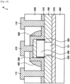
- FIG. 11 is a cross-sectional view showing a multilayer structure of the semiconductor device 3 according to the invention. Note that components indicated by the same reference signs as those of FIG. 1 are substantially the same as those shown in FIG. 1 , and therefore, will not be described herein.
- the semiconductor device 3 according to the invention includes a second conductivity type (e.g., p-type) semiconductor layer 420 which is provided between the barrier layer 310 and the gate electrode 400.
- the semiconductor device 3 according to the present invention has a second conductivity type (e.g. p-type) gate.
- the semiconductor layer 420 is formed of a second conductivity type (e.g., p-type) semiconductor.
- the semiconductor layer 420 may be formed by epitaxially growing GaN doped with Mg, which is a p-type impurity, on the barrier layer 310.
- a second conductivity type (p-type) gate is formed by the semiconductor layer 420 being provided between the barrier layer 310 and the gate electrode 400.
- the semiconductor layer 420 may be formed by doping all or a portion of the barrier layer 310 which is in contact with the gate electrode 400 with Mg, which is a p-type impurity.
- the carrier concentration or band state of the barrier layer 310 is modulated through the p-n junction. Therefore, in the semiconductor device 3 according to the present invention, by applying a voltage to the gate electrode 400, the electron concentration of the two-dimensional electron gas layer 320 can be controlled so that a current flowing between the first electrode 110 and the second electrode 210 is modulated.
- the threshold voltage can be higher than that of the semiconductor device 1 having a Schottky gate shown in FIG. 1 , and therefore, a normally-off operation can be easily achieved.
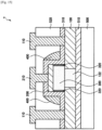
- FIG. 12 is a cross-sectional view showing a multilayer structure of the semiconductor device 4 according to this embodiment. Note that components indicated by the same reference signs as those of FIG. 1 are substantially the same as those shown in FIG. 1 , and therefore, will not be described herein.
- a channel layer 301 is formed of a second conductivity type (e.g., p-type) compound semiconductor material.
- the channel layer 301 may be formed by epitaxially growing GaN doped with Mg, which is a p-type impurity, on the first contact layer 100.
- the potential barrier between the first electrode 110 and the second electrode 210 can be higher than that of the semiconductor device 1 including the i-type (i.e., undoped) channel layer 300 shown in FIG. 1 . Therefore, in the semiconductor device 4 according to this embodiment, a leakage current occurring between the first electrode 110 and the second electrode 210 can be inhibited, compared to the semiconductor device 1 shown in FIG. 1 .
- FIG. 13 is a cross-sectional view showing a multilayer structure of the semiconductor device 5 according to this embodiment. Note that components indicated by the same reference signs as those of FIG. 1 , FIG. 10 , and FIG. 12 are substantially the same as those shown in FIG. 1 , FIG. 10 , and FIG. 12 , and therefore, will not be described herein.
- a gate insulating layer 410 is provided in place of the barrier layer 310, and the channel layer 301 is formed of a second conductivity type (e.g., p-type) compound semiconductor material.
- the semiconductor device 5 according to this embodiment is a field effect transistor which has an MIS gate, and in which an inversion layer formed at an interface of the channel layer 301 which is in contact with the gate insulating layer 410 is a channel.
- a two-dimensional electron gas layer which is formed by a heterojunction of compound semiconductors is not formed, and the inversion layer formed by the MIS gate operates as a channel as in a typical field effect transistor.
- the semiconductor device 5 can be fabricated using a fabrication process easier than that for the semiconductor device 1 shown in FIG. 1 , because it is not necessary to provide the barrier layer 310 which is epitaxially grown and formed.
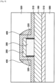
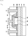
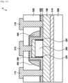
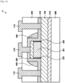
- FIG. 14 to FIG. 16 are cross-sectional views showing a first to a third structure example of the semiconductor device according to this embodiment. Note that components indicated by the same reference signs as those of FIG. 1 are substantially the same as those shown in FIG. 1 , and therefore, will not be described herein.
- a capacitance reduction region is provided in the first contact layer 100 below the channel layer 300 so that a parasitic capacitance (also called an "off-capacitance") during non-operation which occurs by the first contact layer 100 and the second contact layer 200, which have a low resistance, facing each other, can be reduced.
- a parasitic capacitance also called an "off-capacitance”
- the capacitance reduction region is provided in a region smaller than a region where the channel layer 300 is provided in planar view. This is because when the capacitance reduction region is formed in a region having at least the same size as that of the region where the channel layer 300 is provided in planar view, it is difficult to electrically couple the two-dimensional electron gas layer 320 formed on the side surface of the channel layer 300 to the first contact layer 100.
- a low permittivity region 121 having a permittivity lower than that of the first contact layer 100 is provided as a capacitance reduction region in the first contact layer 100 below the channel layer 300.
- the low permittivity region 121 is formed of a material having a permittivity lower than that of the first contact layer 100.
- the low permittivity region 121 may be formed of an insulating material or a cavity.
- the low permittivity region 121 may be formed by removing all or a portion of the first contact layer 100 in the corresponding region using etching or the like, and then forming the channel layer 300 on that region.
- the low permittivity region 121 may be formed by burying an insulating material such as SiO 2 or the like in a region where the first contact layer 100 has been removed by etching or the like.
- the low permittivity region 121 may be formed by etching all or a portion of the first contact layer 100 in the corresponding region from the back surface.
- a portion of the channel layer 300 may also be removed by etching from the back surface.
- the off-capacitance formed by the first contact layer 100 and the second contact layer 200 facing each other can be reduced.
- a parasitic capacitance can be reduced (or alternatively, prevented) from occurring between the first contact layer 100 and the second contact layer 200.
- a low carrier region 122 having a carrier density lower than that of the first contact layer 100 is provided as a capacitance reduction region in the first contact layer 100 below the channel layer 300.
- the low carrier region 122 is configured to have an impurity concentration lower than that of the first contact layer 100.
- the low carrier region 122 may be a layer formed of the same compound semiconductor material as that of the first contact layer 100 that is doped with an n-type impurity (Si, etc.) at a concentration lower than that of the first contact layer 100.
- the low carrier region 122 may be a layer the resistance of which is increased by doping the first contact layer 100 with a p-type impurity (Mg, etc.).
- the low carrier region 122 may be formed by removing all or a portion of the first contact layer 100 in the corresponding region using etching or the like, and regrowing a compound semiconductor at a concentration of an n-type impurity (Si, etc.) lower than that of the first contact layer 100.
- the low carrier region 122 may be formed by additionally doping the first contact layer 100 excluding the low carrier region 122 with an n-type impurity (Si, etc.) by ion injection or the like.
- the low carrier region 122 may be formed by doping the low carrier region 122 with a p-type impurity (Mg, etc.) by ion injection or the like, and thereby increasing the resistance of the low carrier region 122.
- a p-type impurity Mg, etc.
- an off-capacitance formed by the first contact layer 100 and the second contact layer 200 facing each other can be reduced.
- a depletion layer 123 is provided as a capacitance reduction region in the first contact layer 100 below the channel layer 300.
- the depletion layer 123 is formed by a second conductivity type (e.g., p-type) depleted region 130 which is provided in the first contact layer 100.
- the depleted region 130 is obtained by, for example, doping the same compound semiconductor material as that of the first contact layer 100 with a p-type impurity (Mg, etc.).
- the depleted region 130 may be formed by doping the corresponding region of the first contact layer 100 with a p-type impurity (Mg, etc.) by ion injection or the like.
- the depletion layer 123 in which carriers are depleted by a p-n junction is formed below the channel layer 300.
- the depletion layer 123 is formed, extending on both the first contact layer 100 and depleted region 130.
- the carrier density is reduced. Therefore, according to the third structure example, an off-capacitance formed by the first contact layer 100 and the second contact layer 200 facing each other can be reduced, as in the second structure example.
- the depleted region 130 may be floating, although a bias voltage more negative than that of the second electrode 210 may be applied to the depleted region 130 by being in contact with a region outside the device region 600.
- the thickness of the channel layer 300 is the distance between the source electrode and the drain electrode, and therefore, the distance between the source electrode and the drain electrode can be reduced without using state-of-the-art fabrication equipment. Therefore, in the semiconductor device according to one embodiment of the present disclosure, the channel resistance and the on-resistance can be reduced.
- the thickness of the channel layer 300 is the gate length, and therefore, the gate length can be reduced without using state-of-the-art fabrication equipment. Therefore, the semiconductor device can operate at higher speed.
- the side surface of the channel layer 300 formed in an island shape serves as a channel, and therefore, the current density can be increased.
- the size of the semiconductor device according to one embodiment of the present disclosure can be reduced, compared to field effect transistors having other structures.
- a semiconductor device can be applied to electronic parts such as, for example, a radio frequency (RF) module, a power conversion module which uses a high voltage, and the like. Also, a semiconductor device according to one embodiment of the present disclosure can improve the performance of electronic apparatuses including the above electronic parts such as an alternating current (AC) adaptor, power conditioner, smartphone, mobile telephone, and the like.
- RF radio frequency
- AC alternating current
Landscapes
- Junction Field-Effect Transistors (AREA)
- Insulated Gate Type Field-Effect Transistor (AREA)
- Chemical & Material Sciences (AREA)
- Engineering & Computer Science (AREA)
- Materials Engineering (AREA)
Claims (10)
- Halbleitervorrichtung (3), die Folgendes umfasst:ein Substrat (500);eine erste Kontaktschicht (100) auf dem Substrat (500);eine Kanalschicht (300) auf der ersten Kontaktschicht (100), wobei die Kanalschicht eine zweidimensionale Elektronengasschicht (320) auf den Seitenwänden des Kanals (300) in einer Richtung senkrecht zu dem Substrat enthält;eine zweite Kontaktschicht (200) auf der Kanalschicht (300) ;eine Sperrschicht (310) auf der ersten Kontaktschicht (100), auf der zweiten Kontaktschicht und auf den Seitenwänden der Kanalschicht (300);eine Gate-Elektrode (400) auf wenigstens einer Seitenfläche der Sperrschicht (310);eine erste Elektrode (110) auf der ersten Kontaktschicht (100) ;eine zweite Elektrode (210) auf der zweiten Kontaktschicht (200);eine Halbleiterschicht (420) zwischen der Gate-Elektrode (400) und der Sperrschicht (310), wobei die erste Kontaktschicht (100) und die zweite Kontaktschicht (200) von einem ersten Leitfähigkeitstyp sind und die Halbleiterschicht von einem zweiten Leitfähigkeitstyp ist, wobei die Halbleiterschicht (420) ein Gate vom zweiten Leitfähigkeitstyp bildet.
- Halbleitervorrichtung (3) nach Anspruch 1,
wobei eine C-Achsenrichtung eines Kristalls der Kanalschicht im Wesentlichen senkrecht zu einer Seitenfläche der Kanalschicht (300) ist, und/oder wobei die erste Elektrode (110) in der planaren Ansicht um wenigstens drei Seiten der Kanalschicht (300) angeordnet ist. - Halbleitervorrichtung (3) nach Anspruch 1, die ferner Folgendes umfasst:
eine Isolierschicht (520) auf der Gate-Elektrode (400) und der Halbleiterschicht (310). - Halbleitervorrichtung (3) nach Anspruch 1,
wobei die Kanalschicht (300) eine Halbleiterschicht ist. - Halbleitervorrichtung (3) nach Anspruch 1,
wobei die Gate-Elektrode (400) und die zweite Elektrode (210) sich zwischen einem ersten und einem zweiten Abschnitt der ersten Elektrode (110) befinden. - Halbleitervorrichtung (3) nach Anspruch 5,wobei die wenigstens eine Seitenfläche der Sperrschicht (310) eine erste Seitenfläche und eine zweite Seitenfläche aufweist undwobei die Gate-Elektrode (400) einen ersten Abschnitt auf der ersten Seitenfläche und einen zweiten Abschnitt auf der zweiten Seitenfläche aufweist.
- Halbleitervorrichtung (3) nach Anspruch 6,
wobei sich die zweite Elektrode (210) zwischen dem ersten und dem zweiten Abschnitt der Gate-Elektrode (400) befindet. - Elektronisches Bauteil, das Folgendes umfasst:
eine Halbleitervorrichtung nach Anspruch 1. - Elektronische Einrichtung, die Folgendes umfasst:
eine Halbleitervorrichtung nach Anspruch 1. - Verfahren zur Herstellung einer Halbleitervorrichtung (3), das Folgendes umfasst:Bilden einer ersten Kontaktschicht (100) eines ersten Leitfähigkeitstyps auf einem Substrat (500);Bilden einer Kanalschicht (300) auf der ersten Kontaktschicht (100);Bilden einer zweidimensionalen Elektronengasschicht (320) in Seitenwänden der Kanalschicht;Bilden einer zweiten Kontaktschicht (200) des ersten Leitfähigkeitstyps auf der ersten Kontaktschicht (100) und der Kanalschicht (300);Ätzen der Kanalschicht (300) und der zweiten Kontaktschicht (200), um einen Abschnitt der ersten Kontaktschicht (100) freizulegen;Bilden einer Sperrschicht (310) auf dem Abschnitt der ersten Kontaktschicht (100) und der geätzten zweiten Kontaktschicht (200) und auf den Seitenwänden der Kanalschicht; wobei in der Kanalschicht (300) in der Nähe einer Grenzfläche der Kanalschicht (300) mit der Sperrschicht (310) ein 2DEG gebildet wird;Bilden einer Gate-Elektrode (400) auf wenigstens einer Seitenfläche der Sperrschicht (310);Bilden einer ersten Elektrode (110) und einer zweiten Elektrode (210) auf der ersten Kontaktschicht (100) bzw. der zweiten Kontaktschicht (200); undBilden einer Halbleiterschicht (420) zwischen der Gate-Elektrode (400) und der Sperrschicht (310), wobei die erste Kontaktschicht (100) und die zweite Kontaktschicht (200) von einem ersten Leitfähigkeitstyp sind und die Halbleiterschicht von einem zweiten Leitfähigkeitstyp ist, wobei die Halbleiterschicht (420) ein Gate vom zweiten Leitfähigkeitstyp bildet.
Applications Claiming Priority (2)
| Application Number | Priority Date | Filing Date | Title |
|---|---|---|---|
| JP2016009797A JP6693142B2 (ja) | 2016-01-21 | 2016-01-21 | 半導体装置、電子部品、電子機器、および半導体装置の製造方法 |
| PCT/JP2017/001014 WO2017126428A1 (en) | 2016-01-21 | 2017-01-13 | Semiconductor device, electronic part, electronic apparatus, and method for fabricating semiconductor device |
Publications (2)
| Publication Number | Publication Date |
|---|---|
| EP3405979A1 EP3405979A1 (de) | 2018-11-28 |
| EP3405979B1 true EP3405979B1 (de) | 2023-10-11 |
Family
ID=57915035
Family Applications (1)
| Application Number | Title | Priority Date | Filing Date |
|---|---|---|---|
| EP17702170.6A Active EP3405979B1 (de) | 2016-01-21 | 2017-01-13 | Halbleiterbauelement, elektronisches teil, elektronische vorrichtung und verfahren zur herstellung eines halbleiterbauelements |
Country Status (6)
| Country | Link |
|---|---|
| US (1) | US20190035922A1 (de) |
| EP (1) | EP3405979B1 (de) |
| JP (1) | JP6693142B2 (de) |
| CN (1) | CN108352408B (de) |
| TW (1) | TWI732813B (de) |
| WO (1) | WO2017126428A1 (de) |
Families Citing this family (4)
| Publication number | Priority date | Publication date | Assignee | Title |
|---|---|---|---|---|
| US10217819B2 (en) * | 2015-05-20 | 2019-02-26 | Samsung Electronics Co., Ltd. | Semiconductor device including metal-2 dimensional material-semiconductor contact |
| CN115668506A (zh) * | 2020-05-25 | 2023-01-31 | 索尼半导体解决方案公司 | 半导体装置、半导体模块和电子设备 |
| US20240405118A1 (en) * | 2021-02-01 | 2024-12-05 | Sony Semiconductor Solutions Corporation | Semiconductor device, semiconductor module, and electronic apparatus |
| WO2026053620A1 (ja) * | 2024-09-06 | 2026-03-12 | ソニーセミコンダクタソリューションズ株式会社 | ショットキー障壁接合型高電子移動度トランジスタ、半導体装置、半導体モジュール及び電子機器 |
Citations (2)
| Publication number | Priority date | Publication date | Assignee | Title |
|---|---|---|---|---|
| JPH0715018A (ja) * | 1993-06-15 | 1995-01-17 | Toshiba Corp | 電界効果トランジスタ |
| US20010013604A1 (en) * | 2000-01-31 | 2001-08-16 | Sony Corporation | Compound semiconductor device and process for fabricating the same |
Family Cites Families (14)
| Publication number | Priority date | Publication date | Assignee | Title |
|---|---|---|---|---|
| JPH098290A (ja) * | 1995-06-20 | 1997-01-10 | Mitsubishi Electric Corp | 半導体装置及びその製造方法 |
| JP2000208760A (ja) * | 1999-01-13 | 2000-07-28 | Furukawa Electric Co Ltd:The | 電界効果トランジスタ |
| JP2005286140A (ja) * | 2004-03-30 | 2005-10-13 | Seiko Epson Corp | 半導体装置およびその製造方法 |
| WO2007077813A1 (ja) * | 2005-12-28 | 2007-07-12 | Kao Corporation | 柔軟洗剤組成物 |
| JP2008053449A (ja) * | 2006-08-24 | 2008-03-06 | Rohm Co Ltd | 半導体装置およびその製造方法 |
| JP2008218846A (ja) * | 2007-03-06 | 2008-09-18 | Rohm Co Ltd | 窒化物半導体素子および窒化物半導体素子の製造方法 |
| JP2009170746A (ja) * | 2008-01-18 | 2009-07-30 | Toshiba Corp | 半導体装置及びその製造方法 |
| JP5505698B2 (ja) | 2010-02-01 | 2014-05-28 | 日本電信電話株式会社 | 半導体装置 |
| JP2012104568A (ja) * | 2010-11-08 | 2012-05-31 | Sumitomo Electric Ind Ltd | 半導体装置およびその製造方法 |
| JP2012169470A (ja) * | 2011-02-15 | 2012-09-06 | Nippon Telegr & Teleph Corp <Ntt> | 半導体装置およびその製造方法 |
| JP5844656B2 (ja) * | 2012-02-20 | 2016-01-20 | ルネサスエレクトロニクス株式会社 | 半導体装置及び半導体装置の製造方法 |
| JP6069688B2 (ja) * | 2012-06-18 | 2017-02-01 | 富士通株式会社 | 化合物半導体装置及びその製造方法 |
| JP6444045B2 (ja) * | 2014-04-02 | 2018-12-26 | ローム株式会社 | 半導体装置および半導体装置の製造方法 |
| US9871111B2 (en) * | 2014-09-18 | 2018-01-16 | Taiwan Semiconductor Manufacturing Company, Ltd. | Semiconductor device and method |
-
2016
- 2016-01-21 JP JP2016009797A patent/JP6693142B2/ja active Active
-
2017
- 2017-01-12 TW TW106100920A patent/TWI732813B/zh not_active IP Right Cessation
- 2017-01-13 US US16/069,841 patent/US20190035922A1/en not_active Abandoned
- 2017-01-13 WO PCT/JP2017/001014 patent/WO2017126428A1/en not_active Ceased
- 2017-01-13 EP EP17702170.6A patent/EP3405979B1/de active Active
- 2017-01-13 CN CN201780003978.5A patent/CN108352408B/zh active Active
Patent Citations (2)
| Publication number | Priority date | Publication date | Assignee | Title |
|---|---|---|---|---|
| JPH0715018A (ja) * | 1993-06-15 | 1995-01-17 | Toshiba Corp | 電界効果トランジスタ |
| US20010013604A1 (en) * | 2000-01-31 | 2001-08-16 | Sony Corporation | Compound semiconductor device and process for fabricating the same |
Also Published As
| Publication number | Publication date |
|---|---|
| JP2017130579A (ja) | 2017-07-27 |
| TW201737354A (zh) | 2017-10-16 |
| WO2017126428A1 (en) | 2017-07-27 |
| TWI732813B (zh) | 2021-07-11 |
| CN108352408B (zh) | 2021-09-17 |
| US20190035922A1 (en) | 2019-01-31 |
| JP6693142B2 (ja) | 2020-05-13 |
| CN108352408A (zh) | 2018-07-31 |
| EP3405979A1 (de) | 2018-11-28 |
Similar Documents
| Publication | Publication Date | Title |
|---|---|---|
| CN100429786C (zh) | 在基于氮化镓的盖帽区段上有栅接触区的氮化铝镓/氮化镓高电子迁移率晶体管及其制造方法 | |
| US9837519B2 (en) | Semiconductor device | |
| US9837518B2 (en) | Semiconductor device | |
| CN111883588B (zh) | 用于hemt器件的侧壁钝化 | |
| US11335798B2 (en) | Enhancement mode MISHEMT with GaN channel regrowth under a gate area | |
| US8669591B2 (en) | E-mode HFET device | |
| US9184305B2 (en) | Method and system for a GAN vertical JFET utilizing a regrown gate | |
| US8390029B2 (en) | Semiconductor device for reducing and/or preventing current collapse | |
| US10840353B2 (en) | High electron mobility transistor with dual thickness barrier layer | |
| US8164117B2 (en) | Nitride semiconductor device | |
| CN113169228A (zh) | 包括垂直栅极模块的横向iii族氮化物器件 | |
| US10553697B1 (en) | Regrowth method for fabricating wide-bandgap transistors, and devices made thereby | |
| US20130240951A1 (en) | Gallium nitride superjunction devices | |
| KR101092467B1 (ko) | 인헨스먼트 노말리 오프 질화물 반도체 소자 및 그 제조방법 | |
| US20130032812A1 (en) | Method and system for a gan vertical jfet utilizing a regrown channel | |
| KR20150070001A (ko) | 반도체 장치 | |
| US20130214283A1 (en) | Power Transistor Having Segmented Gate | |
| US20120228674A1 (en) | Semiconductor device, field-effect transistor, and electronic device | |
| US11127743B2 (en) | Transistor, semiconductor device, electronic apparatus, and method for producing transistor | |
| CN108352408B (zh) | 半导体装置、电子部件、电子设备以及半导体装置的制造方法 | |
| JP2013239735A (ja) | 電界効果トランジスタ | |
| WO2023219046A1 (ja) | 窒化物半導体装置 |
Legal Events
| Date | Code | Title | Description |
|---|---|---|---|
| STAA | Information on the status of an ep patent application or granted ep patent |
Free format text: STATUS: UNKNOWN |
|
| STAA | Information on the status of an ep patent application or granted ep patent |
Free format text: STATUS: THE INTERNATIONAL PUBLICATION HAS BEEN MADE |
|
| PUAI | Public reference made under article 153(3) epc to a published international application that has entered the european phase |
Free format text: ORIGINAL CODE: 0009012 |
|
| STAA | Information on the status of an ep patent application or granted ep patent |
Free format text: STATUS: REQUEST FOR EXAMINATION WAS MADE |
|
| 17P | Request for examination filed |
Effective date: 20180814 |
|
| AK | Designated contracting states |
Kind code of ref document: A1 Designated state(s): AL AT BE BG CH CY CZ DE DK EE ES FI FR GB GR HR HU IE IS IT LI LT LU LV MC MK MT NL NO PL PT RO RS SE SI SK SM TR |
|
| AX | Request for extension of the european patent |
Extension state: BA ME |
|
| DAV | Request for validation of the european patent (deleted) | ||
| DAX | Request for extension of the european patent (deleted) | ||
| STAA | Information on the status of an ep patent application or granted ep patent |
Free format text: STATUS: EXAMINATION IS IN PROGRESS |
|
| 17Q | First examination report despatched |
Effective date: 20200910 |
|
| RAP3 | Party data changed (applicant data changed or rights of an application transferred) |
Owner name: SONY GROUP CORPORATION |
|
| RIC1 | Information provided on ipc code assigned before grant |
Ipc: H01L 29/10 20060101ALI20230323BHEP Ipc: H01L 29/80 20060101ALI20230323BHEP Ipc: H01L 29/417 20060101ALI20230323BHEP Ipc: H01L 29/20 20060101ALI20230323BHEP Ipc: H01L 21/336 20060101ALI20230323BHEP Ipc: H01L 29/06 20060101ALI20230323BHEP Ipc: H01L 29/423 20060101ALI20230323BHEP Ipc: H01L 29/778 20060101ALI20230323BHEP Ipc: H01L 29/78 20060101AFI20230323BHEP |
|
| GRAP | Despatch of communication of intention to grant a patent |
Free format text: ORIGINAL CODE: EPIDOSNIGR1 |
|
| STAA | Information on the status of an ep patent application or granted ep patent |
Free format text: STATUS: GRANT OF PATENT IS INTENDED |
|
| INTG | Intention to grant announced |
Effective date: 20230502 |
|
| GRAS | Grant fee paid |
Free format text: ORIGINAL CODE: EPIDOSNIGR3 |
|
| GRAA | (expected) grant |
Free format text: ORIGINAL CODE: 0009210 |
|
| STAA | Information on the status of an ep patent application or granted ep patent |
Free format text: STATUS: THE PATENT HAS BEEN GRANTED |
|
| AK | Designated contracting states |
Kind code of ref document: B1 Designated state(s): AL AT BE BG CH CY CZ DE DK EE ES FI FR GB GR HR HU IE IS IT LI LT LU LV MC MK MT NL NO PL PT RO RS SE SI SK SM TR |
|
| REG | Reference to a national code |
Ref country code: GB Ref legal event code: FG4D |
|
| REG | Reference to a national code |
Ref country code: CH Ref legal event code: EP |
|
| REG | Reference to a national code |
Ref country code: DE Ref legal event code: R096 Ref document number: 602017075137 Country of ref document: DE |
|
| REG | Reference to a national code |
Ref country code: IE Ref legal event code: FG4D |
|
| REG | Reference to a national code |
Ref country code: LT Ref legal event code: MG9D |
|
| REG | Reference to a national code |
Ref country code: NL Ref legal event code: MP Effective date: 20231011 |
|
| REG | Reference to a national code |
Ref country code: AT Ref legal event code: MK05 Ref document number: 1621108 Country of ref document: AT Kind code of ref document: T Effective date: 20231011 |
|
| PG25 | Lapsed in a contracting state [announced via postgrant information from national office to epo] |
Ref country code: NL Free format text: LAPSE BECAUSE OF FAILURE TO SUBMIT A TRANSLATION OF THE DESCRIPTION OR TO PAY THE FEE WITHIN THE PRESCRIBED TIME-LIMIT Effective date: 20231011 |
|
| PG25 | Lapsed in a contracting state [announced via postgrant information from national office to epo] |
Ref country code: GR Free format text: LAPSE BECAUSE OF FAILURE TO SUBMIT A TRANSLATION OF THE DESCRIPTION OR TO PAY THE FEE WITHIN THE PRESCRIBED TIME-LIMIT Effective date: 20240112 |
|
| PG25 | Lapsed in a contracting state [announced via postgrant information from national office to epo] |
Ref country code: IS Free format text: LAPSE BECAUSE OF FAILURE TO SUBMIT A TRANSLATION OF THE DESCRIPTION OR TO PAY THE FEE WITHIN THE PRESCRIBED TIME-LIMIT Effective date: 20240211 |
|
| PG25 | Lapsed in a contracting state [announced via postgrant information from national office to epo] |
Ref country code: LT Free format text: LAPSE BECAUSE OF FAILURE TO SUBMIT A TRANSLATION OF THE DESCRIPTION OR TO PAY THE FEE WITHIN THE PRESCRIBED TIME-LIMIT Effective date: 20231011 |
|
| PG25 | Lapsed in a contracting state [announced via postgrant information from national office to epo] |
Ref country code: AT Free format text: LAPSE BECAUSE OF FAILURE TO SUBMIT A TRANSLATION OF THE DESCRIPTION OR TO PAY THE FEE WITHIN THE PRESCRIBED TIME-LIMIT Effective date: 20231011 |
|
| PG25 | Lapsed in a contracting state [announced via postgrant information from national office to epo] |
Ref country code: ES Free format text: LAPSE BECAUSE OF FAILURE TO SUBMIT A TRANSLATION OF THE DESCRIPTION OR TO PAY THE FEE WITHIN THE PRESCRIBED TIME-LIMIT Effective date: 20231011 |
|
| PG25 | Lapsed in a contracting state [announced via postgrant information from national office to epo] |
Ref country code: LT Free format text: LAPSE BECAUSE OF FAILURE TO SUBMIT A TRANSLATION OF THE DESCRIPTION OR TO PAY THE FEE WITHIN THE PRESCRIBED TIME-LIMIT Effective date: 20231011 Ref country code: IS Free format text: LAPSE BECAUSE OF FAILURE TO SUBMIT A TRANSLATION OF THE DESCRIPTION OR TO PAY THE FEE WITHIN THE PRESCRIBED TIME-LIMIT Effective date: 20240211 Ref country code: GR Free format text: LAPSE BECAUSE OF FAILURE TO SUBMIT A TRANSLATION OF THE DESCRIPTION OR TO PAY THE FEE WITHIN THE PRESCRIBED TIME-LIMIT Effective date: 20240112 Ref country code: ES Free format text: LAPSE BECAUSE OF FAILURE TO SUBMIT A TRANSLATION OF THE DESCRIPTION OR TO PAY THE FEE WITHIN THE PRESCRIBED TIME-LIMIT Effective date: 20231011 Ref country code: BG Free format text: LAPSE BECAUSE OF FAILURE TO SUBMIT A TRANSLATION OF THE DESCRIPTION OR TO PAY THE FEE WITHIN THE PRESCRIBED TIME-LIMIT Effective date: 20240111 Ref country code: AT Free format text: LAPSE BECAUSE OF FAILURE TO SUBMIT A TRANSLATION OF THE DESCRIPTION OR TO PAY THE FEE WITHIN THE PRESCRIBED TIME-LIMIT Effective date: 20231011 Ref country code: PT Free format text: LAPSE BECAUSE OF FAILURE TO SUBMIT A TRANSLATION OF THE DESCRIPTION OR TO PAY THE FEE WITHIN THE PRESCRIBED TIME-LIMIT Effective date: 20240212 |
|
| P01 | Opt-out of the competence of the unified patent court (upc) registered |
Effective date: 20240329 |
|
| PG25 | Lapsed in a contracting state [announced via postgrant information from national office to epo] |
Ref country code: SE Free format text: LAPSE BECAUSE OF FAILURE TO SUBMIT A TRANSLATION OF THE DESCRIPTION OR TO PAY THE FEE WITHIN THE PRESCRIBED TIME-LIMIT Effective date: 20231011 Ref country code: RS Free format text: LAPSE BECAUSE OF FAILURE TO SUBMIT A TRANSLATION OF THE DESCRIPTION OR TO PAY THE FEE WITHIN THE PRESCRIBED TIME-LIMIT Effective date: 20231011 Ref country code: PL Free format text: LAPSE BECAUSE OF FAILURE TO SUBMIT A TRANSLATION OF THE DESCRIPTION OR TO PAY THE FEE WITHIN THE PRESCRIBED TIME-LIMIT Effective date: 20231011 Ref country code: NO Free format text: LAPSE BECAUSE OF FAILURE TO SUBMIT A TRANSLATION OF THE DESCRIPTION OR TO PAY THE FEE WITHIN THE PRESCRIBED TIME-LIMIT Effective date: 20240111 Ref country code: LV Free format text: LAPSE BECAUSE OF FAILURE TO SUBMIT A TRANSLATION OF THE DESCRIPTION OR TO PAY THE FEE WITHIN THE PRESCRIBED TIME-LIMIT Effective date: 20231011 Ref country code: HR Free format text: LAPSE BECAUSE OF FAILURE TO SUBMIT A TRANSLATION OF THE DESCRIPTION OR TO PAY THE FEE WITHIN THE PRESCRIBED TIME-LIMIT Effective date: 20231011 |
|
| PG25 | Lapsed in a contracting state [announced via postgrant information from national office to epo] |
Ref country code: DK Free format text: LAPSE BECAUSE OF FAILURE TO SUBMIT A TRANSLATION OF THE DESCRIPTION OR TO PAY THE FEE WITHIN THE PRESCRIBED TIME-LIMIT Effective date: 20231011 |
|
| REG | Reference to a national code |
Ref country code: DE Ref legal event code: R097 Ref document number: 602017075137 Country of ref document: DE |
|
| PG25 | Lapsed in a contracting state [announced via postgrant information from national office to epo] |
Ref country code: CZ Free format text: LAPSE BECAUSE OF FAILURE TO SUBMIT A TRANSLATION OF THE DESCRIPTION OR TO PAY THE FEE WITHIN THE PRESCRIBED TIME-LIMIT Effective date: 20231011 |
|
| PG25 | Lapsed in a contracting state [announced via postgrant information from national office to epo] |
Ref country code: SK Free format text: LAPSE BECAUSE OF FAILURE TO SUBMIT A TRANSLATION OF THE DESCRIPTION OR TO PAY THE FEE WITHIN THE PRESCRIBED TIME-LIMIT Effective date: 20231011 |
|
| PG25 | Lapsed in a contracting state [announced via postgrant information from national office to epo] |
Ref country code: SM Free format text: LAPSE BECAUSE OF FAILURE TO SUBMIT A TRANSLATION OF THE DESCRIPTION OR TO PAY THE FEE WITHIN THE PRESCRIBED TIME-LIMIT Effective date: 20231011 Ref country code: SK Free format text: LAPSE BECAUSE OF FAILURE TO SUBMIT A TRANSLATION OF THE DESCRIPTION OR TO PAY THE FEE WITHIN THE PRESCRIBED TIME-LIMIT Effective date: 20231011 Ref country code: RO Free format text: LAPSE BECAUSE OF FAILURE TO SUBMIT A TRANSLATION OF THE DESCRIPTION OR TO PAY THE FEE WITHIN THE PRESCRIBED TIME-LIMIT Effective date: 20231011 Ref country code: IT Free format text: LAPSE BECAUSE OF FAILURE TO SUBMIT A TRANSLATION OF THE DESCRIPTION OR TO PAY THE FEE WITHIN THE PRESCRIBED TIME-LIMIT Effective date: 20231011 Ref country code: EE Free format text: LAPSE BECAUSE OF FAILURE TO SUBMIT A TRANSLATION OF THE DESCRIPTION OR TO PAY THE FEE WITHIN THE PRESCRIBED TIME-LIMIT Effective date: 20231011 Ref country code: DK Free format text: LAPSE BECAUSE OF FAILURE TO SUBMIT A TRANSLATION OF THE DESCRIPTION OR TO PAY THE FEE WITHIN THE PRESCRIBED TIME-LIMIT Effective date: 20231011 Ref country code: CZ Free format text: LAPSE BECAUSE OF FAILURE TO SUBMIT A TRANSLATION OF THE DESCRIPTION OR TO PAY THE FEE WITHIN THE PRESCRIBED TIME-LIMIT Effective date: 20231011 |
|
| PLBE | No opposition filed within time limit |
Free format text: ORIGINAL CODE: 0009261 |
|
| STAA | Information on the status of an ep patent application or granted ep patent |
Free format text: STATUS: NO OPPOSITION FILED WITHIN TIME LIMIT |
|
| PG25 | Lapsed in a contracting state [announced via postgrant information from national office to epo] |
Ref country code: MC Free format text: LAPSE BECAUSE OF FAILURE TO SUBMIT A TRANSLATION OF THE DESCRIPTION OR TO PAY THE FEE WITHIN THE PRESCRIBED TIME-LIMIT Effective date: 20231011 |
|
| PG25 | Lapsed in a contracting state [announced via postgrant information from national office to epo] |
Ref country code: MC Free format text: LAPSE BECAUSE OF FAILURE TO SUBMIT A TRANSLATION OF THE DESCRIPTION OR TO PAY THE FEE WITHIN THE PRESCRIBED TIME-LIMIT Effective date: 20231011 |
|
| REG | Reference to a national code |
Ref country code: CH Ref legal event code: PL |
|
| PG25 | Lapsed in a contracting state [announced via postgrant information from national office to epo] |
Ref country code: LU Free format text: LAPSE BECAUSE OF NON-PAYMENT OF DUE FEES Effective date: 20240113 |
|
| 26N | No opposition filed |
Effective date: 20240712 |
|
| GBPC | Gb: european patent ceased through non-payment of renewal fee |
Effective date: 20240113 |
|
| PG25 | Lapsed in a contracting state [announced via postgrant information from national office to epo] |
Ref country code: LU Free format text: LAPSE BECAUSE OF NON-PAYMENT OF DUE FEES Effective date: 20240113 |
|
| PG25 | Lapsed in a contracting state [announced via postgrant information from national office to epo] |
Ref country code: GB Free format text: LAPSE BECAUSE OF NON-PAYMENT OF DUE FEES Effective date: 20240113 |
|
| PG25 | Lapsed in a contracting state [announced via postgrant information from national office to epo] |
Ref country code: BE Free format text: LAPSE BECAUSE OF NON-PAYMENT OF DUE FEES Effective date: 20240131 |
|
| PG25 | Lapsed in a contracting state [announced via postgrant information from national office to epo] |
Ref country code: FR Free format text: LAPSE BECAUSE OF NON-PAYMENT OF DUE FEES Effective date: 20240131 |
|
| PG25 | Lapsed in a contracting state [announced via postgrant information from national office to epo] |
Ref country code: CH Free format text: LAPSE BECAUSE OF NON-PAYMENT OF DUE FEES Effective date: 20240131 |
|
| PG25 | Lapsed in a contracting state [announced via postgrant information from national office to epo] |
Ref country code: SI Free format text: LAPSE BECAUSE OF FAILURE TO SUBMIT A TRANSLATION OF THE DESCRIPTION OR TO PAY THE FEE WITHIN THE PRESCRIBED TIME-LIMIT Effective date: 20231011 |
|
| PG25 | Lapsed in a contracting state [announced via postgrant information from national office to epo] |
Ref country code: SI Free format text: LAPSE BECAUSE OF FAILURE TO SUBMIT A TRANSLATION OF THE DESCRIPTION OR TO PAY THE FEE WITHIN THE PRESCRIBED TIME-LIMIT Effective date: 20231011 Ref country code: GB Free format text: LAPSE BECAUSE OF NON-PAYMENT OF DUE FEES Effective date: 20240113 Ref country code: FR Free format text: LAPSE BECAUSE OF NON-PAYMENT OF DUE FEES Effective date: 20240131 Ref country code: CH Free format text: LAPSE BECAUSE OF NON-PAYMENT OF DUE FEES Effective date: 20240131 Ref country code: BE Free format text: LAPSE BECAUSE OF NON-PAYMENT OF DUE FEES Effective date: 20240131 |
|
| REG | Reference to a national code |
Ref country code: BE Ref legal event code: MM Effective date: 20240131 |
|
| REG | Reference to a national code |
Ref country code: DE Ref legal event code: R079 Ref document number: 602017075137 Country of ref document: DE Free format text: PREVIOUS MAIN CLASS: H01L0029780000 Ipc: H10D0030600000 |
|
| PG25 | Lapsed in a contracting state [announced via postgrant information from national office to epo] |
Ref country code: IE Free format text: LAPSE BECAUSE OF NON-PAYMENT OF DUE FEES Effective date: 20240113 |
|
| PG25 | Lapsed in a contracting state [announced via postgrant information from national office to epo] |
Ref country code: IE Free format text: LAPSE BECAUSE OF NON-PAYMENT OF DUE FEES Effective date: 20240113 |
|
| PG25 | Lapsed in a contracting state [announced via postgrant information from national office to epo] |
Ref country code: CY Free format text: LAPSE BECAUSE OF FAILURE TO SUBMIT A TRANSLATION OF THE DESCRIPTION OR TO PAY THE FEE WITHIN THE PRESCRIBED TIME-LIMIT; INVALID AB INITIO Effective date: 20170113 |
|
| PG25 | Lapsed in a contracting state [announced via postgrant information from national office to epo] |
Ref country code: HU Free format text: LAPSE BECAUSE OF FAILURE TO SUBMIT A TRANSLATION OF THE DESCRIPTION OR TO PAY THE FEE WITHIN THE PRESCRIBED TIME-LIMIT; INVALID AB INITIO Effective date: 20170113 |
|
| PG25 | Lapsed in a contracting state [announced via postgrant information from national office to epo] |
Ref country code: FI Free format text: LAPSE BECAUSE OF FAILURE TO SUBMIT A TRANSLATION OF THE DESCRIPTION OR TO PAY THE FEE WITHIN THE PRESCRIBED TIME-LIMIT Effective date: 20231011 |
|
| PG25 | Lapsed in a contracting state [announced via postgrant information from national office to epo] |
Ref country code: TR Free format text: LAPSE BECAUSE OF FAILURE TO SUBMIT A TRANSLATION OF THE DESCRIPTION OR TO PAY THE FEE WITHIN THE PRESCRIBED TIME-LIMIT Effective date: 20231011 |
|
| PGFP | Annual fee paid to national office [announced via postgrant information from national office to epo] |
Ref country code: DE Payment date: 20251217 Year of fee payment: 10 |