EP3091468A1 - Zugriff auf integrierte schaltung - Google Patents
Zugriff auf integrierte schaltung Download PDFInfo
- Publication number
- EP3091468A1 EP3091468A1 EP16167621.8A EP16167621A EP3091468A1 EP 3091468 A1 EP3091468 A1 EP 3091468A1 EP 16167621 A EP16167621 A EP 16167621A EP 3091468 A1 EP3091468 A1 EP 3091468A1
- Authority
- EP
- European Patent Office
- Prior art keywords
- security key
- integrated circuit
- memory
- access
- key
- Prior art date
- Legal status (The legal status is an assumption and is not a legal conclusion. Google has not performed a legal analysis and makes no representation as to the accuracy of the status listed.)
- Granted
Links
Images

Classifications
-
- G—PHYSICS
- G06—COMPUTING OR CALCULATING; COUNTING
- G06F—ELECTRIC DIGITAL DATA PROCESSING
- G06F21/00—Security arrangements for protecting computers, components thereof, programs or data against unauthorised activity
- G06F21/30—Authentication, i.e. establishing the identity or authorisation of security principals
- G06F21/44—Program or device authentication
-
- G—PHYSICS
- G06—COMPUTING OR CALCULATING; COUNTING
- G06F—ELECTRIC DIGITAL DATA PROCESSING
- G06F21/00—Security arrangements for protecting computers, components thereof, programs or data against unauthorised activity
- G06F21/50—Monitoring users, programs or devices to maintain the integrity of platforms, e.g. of processors, firmware or operating systems
- G06F21/57—Certifying or maintaining trusted computer platforms, e.g. secure boots or power-downs, version controls, system software checks, secure updates or assessing vulnerabilities
-
- G—PHYSICS
- G09—EDUCATION; CRYPTOGRAPHY; DISPLAY; ADVERTISING; SEALS
- G09C—CIPHERING OR DECIPHERING APPARATUS FOR CRYPTOGRAPHIC OR OTHER PURPOSES INVOLVING THE NEED FOR SECRECY
- G09C1/00—Apparatus or methods whereby a given sequence of signs, e.g. an intelligible text, is transformed into an unintelligible sequence of signs by transposing the signs or groups of signs or by replacing them by others according to a predetermined system
-
- G—PHYSICS
- G06—COMPUTING OR CALCULATING; COUNTING
- G06F—ELECTRIC DIGITAL DATA PROCESSING
- G06F2221/00—Indexing scheme relating to security arrangements for protecting computers, components thereof, programs or data against unauthorised activity
- G06F2221/21—Indexing scheme relating to G06F21/00 and subgroups addressing additional information or applications relating to security arrangements for protecting computers, components thereof, programs or data against unauthorised activity
- G06F2221/2143—Clearing memory, e.g. to prevent the data from being stolen
Definitions
- This invention relates to integrated circuit access. More in particular, the present invention relates to an integrated circuit configured for providing secure access, as well as to a user device provided with such an integrated circuit and a method of providing secure access to an integrated circuit.
- the integrated circuit includes a memory in which a security key can be stored.
- the security key stored in the memory can be compared with a security key stored in another part of the integrated circuit. Access to the integrated circuit can be granted when the security keys match and can be denied when the security keys fail to match. If the keys fail to match, the memory of the integrated circuit can only be erased, thus erasing the non-matching security key and any other content. After the erase, a new security key can be stored in memory. In this way, it can be ascertained that an integrated circuit is properly initialized.
- circuitry is described in operation. However, it will be apparent that the respective elements are arranged to perform the functions being described as performed by them.
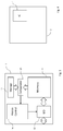
- FIG. 1 An exemplary integrated circuit in accordance with an embodiment of the present invention is schematically illustrated in Fig. 1 .
- the integrated circuit 1 of Fig. 1 includes a memory unit 11, a storage unit 12, a comparator unit 13, an access control unit 14, and an input/output (I/O) unit 15.
- the integrated circuit 1 may include additional components but such components are not shown in Fig. 1 for the sake of clarity of the illustration.
- the memory unit 11 may be a so-called flash memory, a semiconductor memory in which data can be stored but from which the data can also be deleted.
- the memory unit 11 is preferably non-volatile, preserving the stored data when power is off.
- Stored data can be exchanged, via the I/O unit 15, between the memory unit 11 and circuits outside the integrated circuit 1, as shown in Fig. 1 .
- Data stored in the memory unit 11 may also be exchanged, via the I/O unit 15, with other units (not shown in Fig. 1 ) inside the integrated circuit 1.
- the storage unit 12 can be configured for permanently storing a security key.
- a security key for example an embodiment using synthesized logic which provides an unalterable bit pattern as security key.
- a hard-wired and therefore unalterable memory is used which may be referred to as read-only memory.
- Yet another embodiment may include a programmable read-only memory (PROM) having fuses or antifuses that can be blown to permanently store information.
- PROM programmable read-only memory
- the security key in the storage unit 12 will be referred to as first security key.
- the storage unit 12 can be arranged in such a way that its contents can only be read out by the comparator unit 13, not by other units..
- the comparator unit 13 is configured for comparing the contents of the storage unit 12 and the contents of certain locations of the memory unit 11, which contain a second security key. If the contents of the storage unit 12 and the contents of those locations of the memory unit 11 match, then the comparator unit 13 sends a positive comparator signal to the access control unit 14. If the contents of the storage unit 12 and the contents of those locations of the memory unit 11 fail to match, then the comparator unit 13 sends a negative comparator signal to the access control unit 14.
- the terms “positive” and “negative” as used here refer to the meaning of the comparator signal, not to its particular polarity. It is further noted that the match of the contents of the locations of the memory unit 11 and the contents of the storage unit 12 typically but not necessarily means that the first and the second security keys are identical. Embodiments can be envisaged in which only parts of the security keys are compared, and/or in which a predefined deviation of the security keys (for example a limited number of non-identical bits) still results in a match. Additionally, or alternatively, the security keys may be said to match if they have matching transforms, which transforms may or may not be cryptographic transforms. The security keys can have any desired length, for example 16 bits, 32 bits, 64 bits, 128 bits, 256 bits or longer.
- the access control unit 14 can directly grant access by supplying an enable signal to the I/O unit 15 so as to allow the I/O unit to write data to or retrieve data from the memory unit 11.
- the access control unit 14 may continue with a further security check, which involves an access key.
- This access key which typically is distinct from the security key, serves to verify access permissions to memory.
- An access key will typically be received from another device external to the integrated circuit, for example from a keypad or from a computer, and be compared with an access key stored in the memory of the integrated circuit. If the received access key and the stored access key match, for example because they are identical, then access to the memory of the integrated circuit will be granted, otherwise access may be denied.
- the matching of the received access key and the stored access key may be determined using a further comparator (not shown in Fig. 1 for the sake of clarity of the illustration).
- the access key may be stored in memory after initialization of the integrated circuit, for example by an end user. It is noted that the access key will later be further explained with reference to Figs. 2 and 3 .
- the security keys make it possible to distinguish an uninitialized integrated circuit from an initialized one, in particular when the security key has a bit pattern which is very unlikely to occur in uninitialized integrated circuits.
- the access keys make it possible to control access to the memory once the integrated circuit has been initialized. It is noted that different parties may use different keys, for different purposes. An integrated circuits manufacturer, for example, may use the security key while an electronics apparatus manufacturer, who uses the integrated circuits in his products, may use the access key.
- the integrated circuit 1 of Fig. 1 is configured for only allowing access to the memory unit 11 when the access control unit 14, aided by the comparator unit 13, has established that the (second) security key stored in the memory unit 11 matches the (first) security key stored in the storage unit 12.
- This match indicates that the memory contents have not been tampered with. More in particular, this match can be used to establish that the integrated circuit has been properly initialized. This can be accomplished by configuring the integrated circuit 1 in such a way that the absence of a match between the first and second security keys not only inhibits memory access, but all operations related to memory except for a memory erase operation.
- the access control unit 14 can be configured for this purpose, using the comparator signal.
- a memory access verification step in which the validity of an access key is checked, can therefore only be carried out when the security keys are found to match.
- the comparison can be carried out after a reset of the integrated circuit.
- a positive comparator signal that is, matching security keys
- a negative comparator signal that is, non-matching security keys
- the integrated circuit cannot be used before the memory is erased (it is noted that the storage 12 cannot be erased).
- This feature is particularly useful for distinguishing uninitialized or "virgin” integrated circuits from initialized integrated circuits: uninitialized integrated circuits will hold no valid security key in memory, while properly initialized integrated circuits will. Accordingly, all integrated circuits can be initialized by storing a valid security key (matching the unalterable security key) in memory, the initialization requiring a complete erasing of the memory prior to storing the security key.
- This feature is further particularly useful for separating the common access protection which may be implemented using access keys from a type of access protection which only needs to distinguish between an initialized device and an uninitialized device, as is the case directly after manufacture of an integrated circuit.
- a newly manufactured integrated circuit will typically not have a valid access key, but for testing purposes a complete access to the integrated circuit is necessary. By granting access to the integrated circuit after erasing its memory, the availability of an access key is no longer relevant.
- Fig. 1 only a single memory unit 11 is shown, but that the integrated circuit 1 may include more than one memory unit, for example two, four or eight memory units. It will be understood that any erase operation made necessary by a negative comparator signal as described above will typically erase all memory units of the integrated circuit. It will further be understood that the storage 12 will not be affected by such an erase operation.
- the exemplary sequence 100 starts with a reset step 101, in which the integrated circuit is reset.
- a reset step 101 in which the integrated circuit is reset.
- embodiments may be envisaged which do not include a reset step, such an initial step forces the integrated circuit to be in a well-defined state.
- step 102 the validity of the security key stored in memory is checked, that is, a check is made whether the (second) security key retrieved from the memory unit matches the (first) security key in the storage unit. If there is a match ("Yes"), then there is a valid security key and the method continues with step 108, in which the presence of a valid access key in memory may be checked.
- An access key is an additional security measure which may be applied independently from the security key. It is noted that the access key and the security key are preferably two separate, distinct keys stored at different memory locations, and that use of an access key (or access keys) is optional. It is further noted that erasing the memory will also erase the access key. Two or more distinct access keys may be used to control access to different parts of the integrated circuit. If there is a valid access key, or if there are valid access keys, then access to the integrated circuit is granted in step 109. If no valid access key is identified, then access is denied.
- step 102 in which the validity of the security key was checked, if there is no match ("No"), then there is no valid security key (which means that the integrated circuit has not, or not properly, been initialized) and the method continues with step 103.
- step 103 memory operations such as read access and write access are disabled. However, an (initial) erase operation is enabled. As a result, the only enabled memory operation is an (initial) erase operation. It is noted that an initial erase operation typically erases the entire memory so as to initialize the memory, clearing any previous contents.
- step 104 the (initial or other) erase operation is carried out, for example under control of another device, that is, a device other than the integrated circuit concerned.
- the erase operation may also be controlled and initiated by the integrated circuit itself.
- step 105 the erase operation can be checked. If the erase operation was successful, for example when the memory is completely erased, then the sequence continues with step 106. If the erase operation was not successful, then the sequence returns in the present example to step 102 to check the validity of the security key again. This check is certain to fail, leading to step 103 in which the erase operation is enabled again. In some embodiments, the sequence may return directly to step 103.
- step 106 writing to the memory is enabled again, thus reversing the disabling of step 103, to allow the security key to be written in the next step. It is noted that reading from memory may have been enabled in step 105 to allow an erasure check only. As writing to memory is now enabled, the security key can now be written to memory in step 107. As mentioned before, this (second) security key must correspond with the (first) security key in the storage (12 in Fig. 1 ); the second security key may be identical or similar to the first security key.
- the security key stored in memory is proof that the integrated circuit, and in particular its memory, has been properly initialized. After step 107, the sequence returns to step 102 in which the security key is read from memory and checked for validity.
- sequence 100 ensures that the memory access verification step 108 can only be carried out when the memory holds a valid security key.
- FIG. 3 Another embodiment of a portion of an integrated circuit is schematically shown in Fig. 3 .
- the key storage 12 is part of control logic 14 which serves as access control.
- the I/O unit 15 of Fig. 1 is here constituted by a read logic unit 15A and a write logic unit 15B, both of which are controlled by the control logic unit 14 and which allow data to be exchanged with another device 20 which may be located outside the integrated circuit 10.
- the embodiment of Fig. 3 further includes a first flag register (FR) 17 and a second flag register (FR) 18, as well as a reset unit 16.
- the reset unit 16 serves to initiate a reset in response to a reset condition, which may be triggered by an externally provided reset request or by an internal reset condition, which may in turn depend on external input. In response to the reset condition, the reset unit 16 sends a reset signal to the control logic unit 14.
- the first flag register 17 serves as "virgin device flag” and may, for example, store a first value (for example “1") when it has been established that the integrated circuit is uninitialized (that is, "virgin”) and a second value (for example "0") when it is not. This may be accomplished by storing a suitable value in the first flag register in step 102 of the sequence of Fig. 2 upon detection of a valid security key.
- the second flag register 18 stores a flag indicating whether the erase, corresponding with step 105 in the sequence of Fig. 2 , was successful.
- the flag registers 17 & 18 may be protected to prevent access from outside the integrated circuit and thus to prevent tampering. Both flag registers can be reset by a reset of the integrated circuit.
- the second flag register 18 can be connected to both the control logic 14 and the write logic 15B as its flag determines whether the write logic is enabled or not. When the flag of the second flag register 18 is set in the embodiment of Fig. 3 , the write logic 15B can be enabled. Conversely, when the flag of the second flag register 18 is not set, the write logic 15B can be disabled, thus making it impossible to write to the memory 11.
- the second flag register 18 may be set by hardware (the control logic unit 14) after a successful erase operation in which the memory 11 is erased. This erase operation may be a so-called "initial erase" which erases all blocks of the non-volatile memory 11 and may use a subsequent read back to ensure that all blocks are completely erased.
- This read back can use intermittent reads of a non-erased value to be able to detect any fake erase results. This allows identifying voltage attacks which mimic the detection of an erased value during read back.
- the second flag register 18 can also be set when a valid security key has been detected in step 102 of the sequence in Fig. 2 to permit later erase operations.
- the memory 11 can hold the (second) security key in a memory area 11A. This (second) security key can be copied to the memory 11, from the (first) security key in the control logic 14 via the read logic 15A.
- the memory 11 may further store an access key in a memory area 11B. After storing the security key and/or the access key, writing to the memory area 11A and/or the memory area 11B may be disabled to prevent any tampering with the security key.
- the (first) security key and/or the access key may have an equal amount of ones and zeroes. This serves to prevent security attacks based upon counting ones and zeroes, which may be achieved using suitable voltage measurements. Keys having equal amounts of ones and zeros may be obtained by replicating an inverse copy of a key (in which the ones and zeros have been inverted) and thus producing a double length key.
- the memory 11 can be a non-volatile memory which preserves the stored data when the power is off.
- the memory 11 can be written to, in contrast to the storage 12 which cannot be written to and which may therefore be referred to as read-only memory.
- the integrated circuit 10 may be a memory integrated circuit, or an integrated circuit containing a memory but having further components, such as a processor, for other tasks.
- One such task may be cryptographic operations, but the invention may well be applied to integrated circuits designed for other tasks than cryptographic operations.
- the user device 2 is shown to include an integrated circuit (IC) 1, which can be an integrated circuit 1 as illustrated in Fig. 1 or an integrated circuit 10 as illustrated in Fig. 3 .
- IC integrated circuit
- the user device 2 may be a mobile (cellular) telephone device, for example, or a navigation device, and can include further components which are not shown in Fig. 4 .
- Such further components may include a keyboard or touchscreen, a display, a power source, and/or further integrated circuits.
- a method provides secure access to an integrated circuit including an unalterable first security key and a memory, in which memory a second security key can be stored, which method may include checking the second security key by comparing the first security key and the second security key; if the second security key is valid, optionally requesting an access key from an external device and receiving an access key, optionally checking the received access key by comparing the received access key with a stored access key, and providing access to the integrated circuit, optionally in dependence of the received access key being valid; and if the second security key is invalid, restricting memory access to an erase operation, and after the erase operation, storing in the memory a new second security key which corresponds to the first security key.
- the checking of the second security key may be preceded by resetting the integrated circuit, while the erase operation may be followed by checking the erasing for completeness.
- a method is configured for initialising an integrated circuit including an unalterable first security key and a memory, in which memory a second security key may be stored, which method may include erasing the memory, and copying or writing the first security key into the memory.
- the memory is erased completely during the erasing. More in particular, it is preferred that at least all memory locations containing security information are erased, for example the security key, the access key, any further keys and/or confidential data, and any confidential software and/or device configuration information. Additionally, or alternatively, to erasing the entire memory, the copied first security key may be permanently but erasably stored in memory so as to constitute a second security key which may be used for security purposes, e.g. to allow tampering detection.
- an integrated circuit may be provided including a processor, an unalterable first security key and a memory, in which memory a second security key may be stored, which processor may be configured for checking the second security key by comparing the first security key and the second security key; if the second security key is valid, optionally requesting an access key from an external device and receiving an access key, optionally checking the received access key by comparing the received access key with a stored access key, and providing access to the integrated circuit, optionally in dependence on the received access key being valid; and if the second security key is invalid, erasing the memory, and storing in the memory a new second security key which corresponds to the first security key.
- the processor may be configured for resetting the integrated circuit before checking the second security key. Additionally, or alternatively, the second security key may be stored in a protected part of the memory.
- the first security key may be hard-wired.
- the processor may be replaced with dedicated circuits, such as a comparator unit and an access control unit.
- a virgin device will be assumed when no valid security key is detected in the device.
- a virgin device can only be initialized by a procedure which guarantees the erasure of all data in memory. Detection of a valid security key guarantees that the device has been properly initialized.
- connections may be any type of connection suitable to transfer signals from or to the respective nodes, units or devices, for example via intermediate devices. Accordingly, unless implied or stated otherwise the connections may for example be direct connections or indirect connections.
- Devices functionally forming separate devices may be integrated in a single physical device. Also, the units and circuits may be suitably combined in one or more semiconductor devices.
- any reference signs placed between parentheses shall not be construed as limiting the claim.
- the word 'comprising' does not exclude the presence of other elements or steps than those listed in a claim.
- the terms "a” or "an,” as used herein, are defined as one or more than one.
Landscapes
- Engineering & Computer Science (AREA)
- Theoretical Computer Science (AREA)
- Computer Security & Cryptography (AREA)
- Computer Hardware Design (AREA)
- Physics & Mathematics (AREA)
- General Engineering & Computer Science (AREA)
- General Physics & Mathematics (AREA)
- Software Systems (AREA)
- Storage Device Security (AREA)
- Mathematical Physics (AREA)
- Microelectronics & Electronic Packaging (AREA)
Applications Claiming Priority (1)
| Application Number | Priority Date | Filing Date | Title |
|---|---|---|---|
| US14/706,128 US9619647B2 (en) | 2015-05-07 | 2015-05-07 | Integrated circuit access |
Publications (2)
| Publication Number | Publication Date |
|---|---|
| EP3091468A1 true EP3091468A1 (de) | 2016-11-09 |
| EP3091468B1 EP3091468B1 (de) | 2020-07-08 |
Family
ID=55970790
Family Applications (1)
| Application Number | Title | Priority Date | Filing Date |
|---|---|---|---|
| EP16167621.8A Active EP3091468B1 (de) | 2015-05-07 | 2016-04-29 | Zugriff auf integrierte schaltung |
Country Status (2)
| Country | Link |
|---|---|
| US (1) | US9619647B2 (de) |
| EP (1) | EP3091468B1 (de) |
Cited By (1)
| Publication number | Priority date | Publication date | Assignee | Title |
|---|---|---|---|---|
| US20230289301A1 (en) * | 2019-11-07 | 2023-09-14 | Micron Technology, Inc. | Semiconductor device with secure access key and associated methods and systems |
Families Citing this family (2)
| Publication number | Priority date | Publication date | Assignee | Title |
|---|---|---|---|---|
| US10318748B2 (en) * | 2016-09-30 | 2019-06-11 | Intel Corporation | Techniques to protect fuses against non-destructive attacks |
| US10318438B1 (en) | 2017-12-07 | 2019-06-11 | Nuvoton Technology Corporation | Secure memory access using memory read restriction |
Citations (3)
| Publication number | Priority date | Publication date | Assignee | Title |
|---|---|---|---|---|
| US20030131210A1 (en) * | 2001-12-19 | 2003-07-10 | Detlef Mueller | Method and arrangement for the verification of NV fuses as well as a corresponding computer program product and a corresponding computer-readable storage medium |
| US20070237325A1 (en) * | 2006-02-01 | 2007-10-11 | Gershowitz Michael N | Method and apparatus to improve security of cryptographic systems |
| US7940073B1 (en) * | 2008-12-05 | 2011-05-10 | Kovio, Inc. | Deactivation of integrated circuits |
Family Cites Families (16)
| Publication number | Priority date | Publication date | Assignee | Title |
|---|---|---|---|---|
| JPH0484348A (ja) * | 1990-07-27 | 1992-03-17 | Nec Corp | Romデータ保護方式 |
| US6138236A (en) * | 1996-07-01 | 2000-10-24 | Sun Microsystems, Inc. | Method and apparatus for firmware authentication |
| US6367017B1 (en) * | 1996-11-07 | 2002-04-02 | Litronic Inc. | Apparatus and method for providing and authentication system |
| JPH10214232A (ja) * | 1997-01-30 | 1998-08-11 | Rohm Co Ltd | Icカードおよびicカードの運用方法 |
| JPH11109856A (ja) * | 1997-09-30 | 1999-04-23 | Matsushita Electric Ind Co Ltd | 復号装置 |
| US6108789A (en) * | 1998-05-05 | 2000-08-22 | Liberate Technologies | Mechanism for users with internet service provider smart cards to roam among geographically disparate authorized network computer client devices without mediation of a central authority |
| US20030172265A1 (en) * | 2001-05-04 | 2003-09-11 | Vu Son Trung | Method and apparatus for secure processing of cryptographic keys |
| US7444682B2 (en) | 2002-07-03 | 2008-10-28 | Macronix International Co., Ltd. | Security memory device and method for making same |
| US20060041932A1 (en) * | 2004-08-23 | 2006-02-23 | International Business Machines Corporation | Systems and methods for recovering passwords and password-protected data |
| US7623378B1 (en) | 2006-05-02 | 2009-11-24 | Lattice Semiconductor Corporation | Selective programming of non-volatile memory facilitated by security fuses |
| US8117377B2 (en) * | 2007-12-27 | 2012-02-14 | Electronics And Telecommunications Research Institute | Flash memory device having secure file deletion function and method for securely deleting flash file |
| US8175276B2 (en) | 2008-02-04 | 2012-05-08 | Freescale Semiconductor, Inc. | Encryption apparatus with diverse key retention schemes |
| US8484486B2 (en) | 2008-08-06 | 2013-07-09 | Silver Spring Networks, Inc. | Integrated cryptographic security module for a network node |
| CN102315933B (zh) * | 2011-10-18 | 2014-02-05 | 飞天诚信科技股份有限公司 | 一种更新密钥的方法及系统 |
| US8938626B2 (en) | 2012-07-17 | 2015-01-20 | Dell Products, L.P. | Single command functionality for providing data security and preventing data access within a decommissioned information handling system |
| US9253200B2 (en) * | 2013-10-28 | 2016-02-02 | GM Global Technology Operations LLC | Programming vehicle modules from remote devices and related methods and systems |
-
2015
- 2015-05-07 US US14/706,128 patent/US9619647B2/en active Active
-
2016
- 2016-04-29 EP EP16167621.8A patent/EP3091468B1/de active Active
Patent Citations (3)
| Publication number | Priority date | Publication date | Assignee | Title |
|---|---|---|---|---|
| US20030131210A1 (en) * | 2001-12-19 | 2003-07-10 | Detlef Mueller | Method and arrangement for the verification of NV fuses as well as a corresponding computer program product and a corresponding computer-readable storage medium |
| US20070237325A1 (en) * | 2006-02-01 | 2007-10-11 | Gershowitz Michael N | Method and apparatus to improve security of cryptographic systems |
| US7940073B1 (en) * | 2008-12-05 | 2011-05-10 | Kovio, Inc. | Deactivation of integrated circuits |
Cited By (2)
| Publication number | Priority date | Publication date | Assignee | Title |
|---|---|---|---|---|
| US20230289301A1 (en) * | 2019-11-07 | 2023-09-14 | Micron Technology, Inc. | Semiconductor device with secure access key and associated methods and systems |
| US12105644B2 (en) * | 2019-11-07 | 2024-10-01 | Lodestar Licensing Group Llc | Semiconductor device with secure access key and associated methods and systems |
Also Published As
| Publication number | Publication date |
|---|---|
| US9619647B2 (en) | 2017-04-11 |
| US20160328554A1 (en) | 2016-11-10 |
| EP3091468B1 (de) | 2020-07-08 |
Similar Documents
| Publication | Publication Date | Title |
|---|---|---|
| US11880313B2 (en) | Storage system and method for performing and authenticating write-protection thereof | |
| US10911229B2 (en) | Unchangeable physical unclonable function in non-volatile memory | |
| US20240354417A1 (en) | Deriving Identity and Root Keys for Embedded Systems | |
| US9984007B2 (en) | Storage system and method for performing and authenticating write-protection thereof | |
| CN110020561B (zh) | 半导体装置和操作半导体装置的方法 | |
| US20080148001A1 (en) | Virtual Secure On-Chip One Time Programming | |
| US8230495B2 (en) | Method for security in electronically fused encryption keys | |
| JP6518798B2 (ja) | 安全な集積回路状態を管理する装置およびその方法 | |
| US20230188326A1 (en) | System on chip, security system, and method of performing authentication | |
| US11106829B2 (en) | Chip fingerprint management based upon one-time programmable memory | |
| US20060184799A1 (en) | Security circuit and method to secure information in a device | |
| EP3091468B1 (de) | Zugriff auf integrierte schaltung | |
| EP3407336A1 (de) | Unveränderliche, physische, nicht klonbare funktion in einem nichtflüchtigen speicher | |
| CN103914664A (zh) | 具有内部存储体保护功能的控制器与控制方法 | |
| US20040186947A1 (en) | Access control system for nonvolatile memory | |
| KR20170102285A (ko) | 보안 요소 | |
| CN111199023A (zh) | 一种mcu程序的密钥系统及解密方法 | |
| US20060221718A1 (en) | Memory module and memory system having data protection function, and method for controlling the memory module | |
| US12500147B2 (en) | Integrated circuit (IC) and electronic apparatus | |
| JP2003203012A (ja) | マイクロコンピュータ装置 | |
| EP4610984A1 (de) | Sicherer nichtflüchtiger speicher und integrierte schaltung mit dem nichtflüchtigen speicher | |
| Zilberstein et al. | e. MMC Security Methods | |
| US10719615B2 (en) | Information processing apparatus, reading control method, and computer readable storage medium | |
| KR102195274B1 (ko) | 보안 모듈의 메모리 관리 | |
| JP2000259801A (ja) | 初期化機能付きicカード用メモリ装置 |
Legal Events
| Date | Code | Title | Description |
|---|---|---|---|
| PUAI | Public reference made under article 153(3) epc to a published international application that has entered the european phase |
Free format text: ORIGINAL CODE: 0009012 |
|
| AK | Designated contracting states |
Kind code of ref document: A1 Designated state(s): AL AT BE BG CH CY CZ DE DK EE ES FI FR GB GR HR HU IE IS IT LI LT LU LV MC MK MT NL NO PL PT RO RS SE SI SK SM TR |
|
| AX | Request for extension of the european patent |
Extension state: BA ME |
|
| RAP1 | Party data changed (applicant data changed or rights of an application transferred) |
Owner name: NXP USA, INC. |
|
| STAA | Information on the status of an ep patent application or granted ep patent |
Free format text: STATUS: REQUEST FOR EXAMINATION WAS MADE |
|
| 17P | Request for examination filed |
Effective date: 20170509 |
|
| RBV | Designated contracting states (corrected) |
Designated state(s): AL AT BE BG CH CY CZ DE DK EE ES FI FR GB GR HR HU IE IS IT LI LT LU LV MC MK MT NL NO PL PT RO RS SE SI SK SM TR |
|
| STAA | Information on the status of an ep patent application or granted ep patent |
Free format text: STATUS: EXAMINATION IS IN PROGRESS |
|
| 17Q | First examination report despatched |
Effective date: 20181017 |
|
| GRAP | Despatch of communication of intention to grant a patent |
Free format text: ORIGINAL CODE: EPIDOSNIGR1 |
|
| STAA | Information on the status of an ep patent application or granted ep patent |
Free format text: STATUS: GRANT OF PATENT IS INTENDED |
|
| INTG | Intention to grant announced |
Effective date: 20200324 |
|
| GRAS | Grant fee paid |
Free format text: ORIGINAL CODE: EPIDOSNIGR3 |
|
| GRAA | (expected) grant |
Free format text: ORIGINAL CODE: 0009210 |
|
| STAA | Information on the status of an ep patent application or granted ep patent |
Free format text: STATUS: THE PATENT HAS BEEN GRANTED |
|
| AK | Designated contracting states |
Kind code of ref document: B1 Designated state(s): AL AT BE BG CH CY CZ DE DK EE ES FI FR GB GR HR HU IE IS IT LI LT LU LV MC MK MT NL NO PL PT RO RS SE SI SK SM TR |
|
| REG | Reference to a national code |
Ref country code: CH Ref legal event code: EP Ref country code: AT Ref legal event code: REF Ref document number: 1289236 Country of ref document: AT Kind code of ref document: T Effective date: 20200715 |
|
| REG | Reference to a national code |
Ref country code: DE Ref legal event code: R096 Ref document number: 602016039386 Country of ref document: DE |
|
| REG | Reference to a national code |
Ref country code: IE Ref legal event code: FG4D |
|
| REG | Reference to a national code |
Ref country code: LT Ref legal event code: MG4D |
|
| REG | Reference to a national code |
Ref country code: AT Ref legal event code: MK05 Ref document number: 1289236 Country of ref document: AT Kind code of ref document: T Effective date: 20200708 |
|
| REG | Reference to a national code |
Ref country code: NL Ref legal event code: MP Effective date: 20200708 |
|
| PG25 | Lapsed in a contracting state [announced via postgrant information from national office to epo] |
Ref country code: NO Free format text: LAPSE BECAUSE OF FAILURE TO SUBMIT A TRANSLATION OF THE DESCRIPTION OR TO PAY THE FEE WITHIN THE PRESCRIBED TIME-LIMIT Effective date: 20201008 Ref country code: BG Free format text: LAPSE BECAUSE OF FAILURE TO SUBMIT A TRANSLATION OF THE DESCRIPTION OR TO PAY THE FEE WITHIN THE PRESCRIBED TIME-LIMIT Effective date: 20201008 Ref country code: LT Free format text: LAPSE BECAUSE OF FAILURE TO SUBMIT A TRANSLATION OF THE DESCRIPTION OR TO PAY THE FEE WITHIN THE PRESCRIBED TIME-LIMIT Effective date: 20200708 Ref country code: PT Free format text: LAPSE BECAUSE OF FAILURE TO SUBMIT A TRANSLATION OF THE DESCRIPTION OR TO PAY THE FEE WITHIN THE PRESCRIBED TIME-LIMIT Effective date: 20201109 Ref country code: ES Free format text: LAPSE BECAUSE OF FAILURE TO SUBMIT A TRANSLATION OF THE DESCRIPTION OR TO PAY THE FEE WITHIN THE PRESCRIBED TIME-LIMIT Effective date: 20200708 Ref country code: HR Free format text: LAPSE BECAUSE OF FAILURE TO SUBMIT A TRANSLATION OF THE DESCRIPTION OR TO PAY THE FEE WITHIN THE PRESCRIBED TIME-LIMIT Effective date: 20200708 Ref country code: AT Free format text: LAPSE BECAUSE OF FAILURE TO SUBMIT A TRANSLATION OF THE DESCRIPTION OR TO PAY THE FEE WITHIN THE PRESCRIBED TIME-LIMIT Effective date: 20200708 Ref country code: SE Free format text: LAPSE BECAUSE OF FAILURE TO SUBMIT A TRANSLATION OF THE DESCRIPTION OR TO PAY THE FEE WITHIN THE PRESCRIBED TIME-LIMIT Effective date: 20200708 Ref country code: GR Free format text: LAPSE BECAUSE OF FAILURE TO SUBMIT A TRANSLATION OF THE DESCRIPTION OR TO PAY THE FEE WITHIN THE PRESCRIBED TIME-LIMIT Effective date: 20201009 Ref country code: FI Free format text: LAPSE BECAUSE OF FAILURE TO SUBMIT A TRANSLATION OF THE DESCRIPTION OR TO PAY THE FEE WITHIN THE PRESCRIBED TIME-LIMIT Effective date: 20200708 |
|
| PG25 | Lapsed in a contracting state [announced via postgrant information from national office to epo] |
Ref country code: RS Free format text: LAPSE BECAUSE OF FAILURE TO SUBMIT A TRANSLATION OF THE DESCRIPTION OR TO PAY THE FEE WITHIN THE PRESCRIBED TIME-LIMIT Effective date: 20200708 Ref country code: PL Free format text: LAPSE BECAUSE OF FAILURE TO SUBMIT A TRANSLATION OF THE DESCRIPTION OR TO PAY THE FEE WITHIN THE PRESCRIBED TIME-LIMIT Effective date: 20200708 Ref country code: LV Free format text: LAPSE BECAUSE OF FAILURE TO SUBMIT A TRANSLATION OF THE DESCRIPTION OR TO PAY THE FEE WITHIN THE PRESCRIBED TIME-LIMIT Effective date: 20200708 Ref country code: IS Free format text: LAPSE BECAUSE OF FAILURE TO SUBMIT A TRANSLATION OF THE DESCRIPTION OR TO PAY THE FEE WITHIN THE PRESCRIBED TIME-LIMIT Effective date: 20201108 |
|
| PG25 | Lapsed in a contracting state [announced via postgrant information from national office to epo] |
Ref country code: NL Free format text: LAPSE BECAUSE OF FAILURE TO SUBMIT A TRANSLATION OF THE DESCRIPTION OR TO PAY THE FEE WITHIN THE PRESCRIBED TIME-LIMIT Effective date: 20200708 |
|
| REG | Reference to a national code |
Ref country code: DE Ref legal event code: R097 Ref document number: 602016039386 Country of ref document: DE |
|
| PG25 | Lapsed in a contracting state [announced via postgrant information from national office to epo] |
Ref country code: IT Free format text: LAPSE BECAUSE OF FAILURE TO SUBMIT A TRANSLATION OF THE DESCRIPTION OR TO PAY THE FEE WITHIN THE PRESCRIBED TIME-LIMIT Effective date: 20200708 Ref country code: DK Free format text: LAPSE BECAUSE OF FAILURE TO SUBMIT A TRANSLATION OF THE DESCRIPTION OR TO PAY THE FEE WITHIN THE PRESCRIBED TIME-LIMIT Effective date: 20200708 Ref country code: CZ Free format text: LAPSE BECAUSE OF FAILURE TO SUBMIT A TRANSLATION OF THE DESCRIPTION OR TO PAY THE FEE WITHIN THE PRESCRIBED TIME-LIMIT Effective date: 20200708 Ref country code: SM Free format text: LAPSE BECAUSE OF FAILURE TO SUBMIT A TRANSLATION OF THE DESCRIPTION OR TO PAY THE FEE WITHIN THE PRESCRIBED TIME-LIMIT Effective date: 20200708 Ref country code: RO Free format text: LAPSE BECAUSE OF FAILURE TO SUBMIT A TRANSLATION OF THE DESCRIPTION OR TO PAY THE FEE WITHIN THE PRESCRIBED TIME-LIMIT Effective date: 20200708 Ref country code: EE Free format text: LAPSE BECAUSE OF FAILURE TO SUBMIT A TRANSLATION OF THE DESCRIPTION OR TO PAY THE FEE WITHIN THE PRESCRIBED TIME-LIMIT Effective date: 20200708 |
|
| PLBE | No opposition filed within time limit |
Free format text: ORIGINAL CODE: 0009261 |
|
| STAA | Information on the status of an ep patent application or granted ep patent |
Free format text: STATUS: NO OPPOSITION FILED WITHIN TIME LIMIT |
|
| PG25 | Lapsed in a contracting state [announced via postgrant information from national office to epo] |
Ref country code: AL Free format text: LAPSE BECAUSE OF FAILURE TO SUBMIT A TRANSLATION OF THE DESCRIPTION OR TO PAY THE FEE WITHIN THE PRESCRIBED TIME-LIMIT Effective date: 20200708 |
|
| 26N | No opposition filed |
Effective date: 20210409 |
|
| PG25 | Lapsed in a contracting state [announced via postgrant information from national office to epo] |
Ref country code: SK Free format text: LAPSE BECAUSE OF FAILURE TO SUBMIT A TRANSLATION OF THE DESCRIPTION OR TO PAY THE FEE WITHIN THE PRESCRIBED TIME-LIMIT Effective date: 20200708 |
|
| PG25 | Lapsed in a contracting state [announced via postgrant information from national office to epo] |
Ref country code: SI Free format text: LAPSE BECAUSE OF FAILURE TO SUBMIT A TRANSLATION OF THE DESCRIPTION OR TO PAY THE FEE WITHIN THE PRESCRIBED TIME-LIMIT Effective date: 20200708 |
|
| PG25 | Lapsed in a contracting state [announced via postgrant information from national office to epo] |
Ref country code: MC Free format text: LAPSE BECAUSE OF FAILURE TO SUBMIT A TRANSLATION OF THE DESCRIPTION OR TO PAY THE FEE WITHIN THE PRESCRIBED TIME-LIMIT Effective date: 20200708 |
|
| GBPC | Gb: european patent ceased through non-payment of renewal fee |
Effective date: 20210429 |
|
| PG25 | Lapsed in a contracting state [announced via postgrant information from national office to epo] |
Ref country code: LU Free format text: LAPSE BECAUSE OF NON-PAYMENT OF DUE FEES Effective date: 20210429 |
|
| REG | Reference to a national code |
Ref country code: BE Ref legal event code: MM Effective date: 20210430 |
|
| PG25 | Lapsed in a contracting state [announced via postgrant information from national office to epo] |
Ref country code: GB Free format text: LAPSE BECAUSE OF NON-PAYMENT OF DUE FEES Effective date: 20210429 Ref country code: FR Free format text: LAPSE BECAUSE OF NON-PAYMENT OF DUE FEES Effective date: 20210430 Ref country code: LI Free format text: LAPSE BECAUSE OF NON-PAYMENT OF DUE FEES Effective date: 20210430 Ref country code: CH Free format text: LAPSE BECAUSE OF NON-PAYMENT OF DUE FEES Effective date: 20210430 |
|
| PG25 | Lapsed in a contracting state [announced via postgrant information from national office to epo] |
Ref country code: IE Free format text: LAPSE BECAUSE OF NON-PAYMENT OF DUE FEES Effective date: 20210429 |
|
| PG25 | Lapsed in a contracting state [announced via postgrant information from national office to epo] |
Ref country code: IS Free format text: LAPSE BECAUSE OF FAILURE TO SUBMIT A TRANSLATION OF THE DESCRIPTION OR TO PAY THE FEE WITHIN THE PRESCRIBED TIME-LIMIT Effective date: 20201108 |
|
| PG25 | Lapsed in a contracting state [announced via postgrant information from national office to epo] |
Ref country code: BE Free format text: LAPSE BECAUSE OF NON-PAYMENT OF DUE FEES Effective date: 20210430 |
|
| PG25 | Lapsed in a contracting state [announced via postgrant information from national office to epo] |
Ref country code: HU Free format text: LAPSE BECAUSE OF FAILURE TO SUBMIT A TRANSLATION OF THE DESCRIPTION OR TO PAY THE FEE WITHIN THE PRESCRIBED TIME-LIMIT; INVALID AB INITIO Effective date: 20160429 |
|
| PG25 | Lapsed in a contracting state [announced via postgrant information from national office to epo] |
Ref country code: CY Free format text: LAPSE BECAUSE OF FAILURE TO SUBMIT A TRANSLATION OF THE DESCRIPTION OR TO PAY THE FEE WITHIN THE PRESCRIBED TIME-LIMIT Effective date: 20200708 |
|
| P01 | Opt-out of the competence of the unified patent court (upc) registered |
Effective date: 20230725 |
|
| PG25 | Lapsed in a contracting state [announced via postgrant information from national office to epo] |
Ref country code: MK Free format text: LAPSE BECAUSE OF FAILURE TO SUBMIT A TRANSLATION OF THE DESCRIPTION OR TO PAY THE FEE WITHIN THE PRESCRIBED TIME-LIMIT Effective date: 20200708 |
|
| PG25 | Lapsed in a contracting state [announced via postgrant information from national office to epo] |
Ref country code: MT Free format text: LAPSE BECAUSE OF FAILURE TO SUBMIT A TRANSLATION OF THE DESCRIPTION OR TO PAY THE FEE WITHIN THE PRESCRIBED TIME-LIMIT Effective date: 20200708 |
|
| PGFP | Annual fee paid to national office [announced via postgrant information from national office to epo] |
Ref country code: DE Payment date: 20250319 Year of fee payment: 10 |
|
| PG25 | Lapsed in a contracting state [announced via postgrant information from national office to epo] |
Ref country code: TR Free format text: LAPSE BECAUSE OF FAILURE TO SUBMIT A TRANSLATION OF THE DESCRIPTION OR TO PAY THE FEE WITHIN THE PRESCRIBED TIME-LIMIT Effective date: 20200708 |