EP3096437B1 - Vorrichtung zur drahtlosen stromübertragung und verfahren zur drahtlosen stromübertragung - Google Patents
Vorrichtung zur drahtlosen stromübertragung und verfahren zur drahtlosen stromübertragung Download PDFInfo
- Publication number
- EP3096437B1 EP3096437B1 EP15734986.1A EP15734986A EP3096437B1 EP 3096437 B1 EP3096437 B1 EP 3096437B1 EP 15734986 A EP15734986 A EP 15734986A EP 3096437 B1 EP3096437 B1 EP 3096437B1
- Authority
- EP
- European Patent Office
- Prior art keywords
- power
- duty ratio
- transmitter
- control
- power conversion
- Prior art date
- Legal status (The legal status is an assumption and is not a legal conclusion. Google has not performed a legal analysis and makes no representation as to the accuracy of the status listed.)
- Not-in-force
Links
Images



Classifications
-
- H—ELECTRICITY
- H02—GENERATION; CONVERSION OR DISTRIBUTION OF ELECTRIC POWER
- H02J—ELECTRIC POWER NETWORKS; CIRCUIT ARRANGEMENTS OR SYSTEMS FOR SUPPLYING OR DISTRIBUTING ELECTRIC POWER; SYSTEMS FOR STORING ELECTRIC ENERGY
- H02J50/00—Circuit arrangements or systems for wireless supply or distribution of electric power
- H02J50/10—Circuit arrangements or systems for wireless supply or distribution of electric power using inductive coupling
- H02J50/12—Circuit arrangements or systems for wireless supply or distribution of electric power using inductive coupling of the resonant type
-
- H—ELECTRICITY
- H02—GENERATION; CONVERSION OR DISTRIBUTION OF ELECTRIC POWER
- H02J—ELECTRIC POWER NETWORKS; CIRCUIT ARRANGEMENTS OR SYSTEMS FOR SUPPLYING OR DISTRIBUTING ELECTRIC POWER; SYSTEMS FOR STORING ELECTRIC ENERGY
- H02J50/00—Circuit arrangements or systems for wireless supply or distribution of electric power
- H02J50/40—Circuit arrangements or systems for wireless supply or distribution of electric power using two or more transmitting or receiving devices
-
- H—ELECTRICITY
- H02—GENERATION; CONVERSION OR DISTRIBUTION OF ELECTRIC POWER
- H02J—ELECTRIC POWER NETWORKS; CIRCUIT ARRANGEMENTS OR SYSTEMS FOR SUPPLYING OR DISTRIBUTING ELECTRIC POWER; SYSTEMS FOR STORING ELECTRIC ENERGY
- H02J7/00—Circuit arrangements for charging or discharging batteries or for supplying loads from batteries
- H02J7/40—Circuit arrangements for charging or discharging batteries or for supplying loads from batteries characterised by the exchange of charge or discharge related data
- H02J7/42—Circuit arrangements for charging or discharging batteries or for supplying loads from batteries characterised by the exchange of charge or discharge related data with electronic devices having internal batteries, e.g. mobile phones
-
- H—ELECTRICITY
- H02—GENERATION; CONVERSION OR DISTRIBUTION OF ELECTRIC POWER
- H02J—ELECTRIC POWER NETWORKS; CIRCUIT ARRANGEMENTS OR SYSTEMS FOR SUPPLYING OR DISTRIBUTING ELECTRIC POWER; SYSTEMS FOR STORING ELECTRIC ENERGY
- H02J7/00—Circuit arrangements for charging or discharging batteries or for supplying loads from batteries
- H02J7/90—Regulation of charging or discharging current or voltage
- H02J7/92—Regulation of charging or discharging current or voltage with prioritisation of loads or sources
-
- H—ELECTRICITY
- H04—ELECTRIC COMMUNICATION TECHNIQUE
- H04B—TRANSMISSION
- H04B5/00—Near-field transmission systems, e.g. inductive or capacitive transmission systems
- H04B5/20—Near-field transmission systems, e.g. inductive or capacitive transmission systems characterised by the transmission technique; characterised by the transmission medium
- H04B5/24—Inductive coupling
-
- H—ELECTRICITY
- H04—ELECTRIC COMMUNICATION TECHNIQUE
- H04B—TRANSMISSION
- H04B5/00—Near-field transmission systems, e.g. inductive or capacitive transmission systems
- H04B5/70—Near-field transmission systems, e.g. inductive or capacitive transmission systems specially adapted for specific purposes
- H04B5/79—Near-field transmission systems, e.g. inductive or capacitive transmission systems specially adapted for specific purposes for data transfer in combination with power transfer
-
- H—ELECTRICITY
- H02—GENERATION; CONVERSION OR DISTRIBUTION OF ELECTRIC POWER
- H02J—ELECTRIC POWER NETWORKS; CIRCUIT ARRANGEMENTS OR SYSTEMS FOR SUPPLYING OR DISTRIBUTING ELECTRIC POWER; SYSTEMS FOR STORING ELECTRIC ENERGY
- H02J50/00—Circuit arrangements or systems for wireless supply or distribution of electric power
- H02J50/80—Circuit arrangements or systems for wireless supply or distribution of electric power involving the exchange of data, concerning supply or distribution of electric power, between transmitting devices and receiving devices
Definitions
- the invention relates to a transmitter for generating power and a method for driving a wirless power transfer system.
- Wireless power transfer (WPT) system is a technology of transferring power through a space without any wire, which maximizes ease of providing mobile equipment and digital appliances with power.
- the wireless power transfer system has advantages of saving energy by a power usage control in real time, overcoming a restriction of space needed for providing power and reducing waste batteries by recharging batteries.
- the wireless power transfer system is typically embodied in a magnetic induction scheme or a magnetic resonance scheme.
- the magnetic induction scheme is a non-contact energy transfer technique where current is applied to one of two coils disposed closely each other and by means of the magnetic flux generated accordingly electromotive force is also applied to the other coil, which may use frequencies of hundreds of kHz.
- the magnetic resonance scheme is a magnetic resonance technique where electric field or magnetic field only is used without using electromagnetic waves or current so that the distance of power transfer is more than several meters, which has a characteristic that band having tens of MHz is used.
- spurious wave that is, a harmonic coming from a power transmitter
- harmonic component may cause an electromagnetic interference effect, thereby having a harmful effect on a body.
- the harmonic refers to a frequency higher than a commercial frequency in terms of power, hundreds of Hz or higher, for example, which has integer multiple frequency of a fundamental.
- the wireless power transfer system generates the harmonic component near the multiple frequency of the receiving frequency due to a non-linear characteristic of the receiver load, basically. That is, the AC signal provided from the receiver does not remain as its waveform but is distorted due to the non-linear load, forming a harmonic.
- the harmonic component disturbs normal operations of surrounding equipment or causes undesired power reception, noise and various obstacles.
- changes of magnetic field emitting from the power transmitter generate current caused by electromagnetic induction phenomenon in a conductor of a stationary surrounding equipment, capable of causing abnormal operations.
- magnetic field generated in the power transmitter causes current in a mobile equipment when the mobile equipment moves around the magnetic field, capable of causing obstacles.
- the power transmitter has a resonance condition similar to that of the surrounding equipment that does not want to receive power, there may occur a magnetic resonance coupling, capable of causing erroneous operations in the surrounding equipment.
- WO 2013/179763 A1 discloses a wireless electric power supply which supplies electric power between a power transmission coil and the receiving coil.
- An inverter has switching elements and converts electric power from the power supply. It supplies power to the transmission coil.
- the electric power supply comprises inverter output current detecting means which detect the output current of said inverter.
- the inverter control means set the pulse width of the target value of the output voltage of the inverter.
- the inverter control means control said inverter according to the output current.
- JP 2013-106490 discloses a solution for the problem to control a power signal in wide dynamic range.
- a resonant antenna includes a transmission coil and a resonant capacitor for transmitting signals that are provided in series.
- a DC power supply applies a DC voltage between a first power-supply line and a second power-supply line.
- a H-bridge circuit is provided between the first power-supply line and the second power-supply line.
- a control unit switches switches by a transmission frequency. The control unit adjusts a phase difference according to the strength of the power signal to be transmitted.
- FIG. 1 is a block diagram of a transmitter for transmitting power in a conventional wireless power transfer system.
- the transmitter 1 may include a gate driver 2, a power converter 3 of a half bridge type, a matching circuit 4, and a transmission coil 5.
- a half bridge circuit of the power converter 3 in the art has two switches that are complementarily turned on and turned off when proper voltage waveforms are applied to gage driving inputs, respectively.
- a square wave voltage generates which is used to switch between a common node of the two switches and the ground.
- the Invention according to claim 1 refers to a transmitter for generating a wireless power to be transmitted to a receiver, the transmitter comprising:
- the device is capable of minimizing current wasted or consumed and enhancing a wireless power transfer efficiency.
- the device solves obstacles such as power reception and noise due to harmonic components included in an output signal of a power conversion part of a transmitter for transmitting power.
- Another embodiment of the present disclosure provides a device that approximates an output waveform of the power conversion part to a sign wave using the power conversion part including a full bridge inverter, improving a harmonic distortion ratio.
- Yet another embodiment of the present disclosure provides a device that feedbacks an output signal outputted from a power conversion part to measure a distribution of harmonic elements of the output signal and to provide a duty ratio that is capable of minimizing the harmonic components.
- the invention according to claim 5 refers to method for driving a wireless power transfer system that includes a transmitter having a power conversion part to convert power applied from an external power supply and a receiver to receive power from the transmitter, the method comprising:
- An embodiment of the present disclosure may change an AC power control signal to control an AC power generator depending on a receiving status of a receiver, and control a duty ratio of an AC voltage of an AC power outputted from an AC power generator in response to the change of the AC power control signal to control the magnitude of the AC power, thereby blocking an occurrence of current loss to prevent power from being wasted.
- An embodiment of the present disclosure may solve obstacles such as power reception and noise due to harmonic components included in an output signal of a power conversion part of a transmission part for transmitting power, improve a harmonic distortion ratio by approximating an output waveform of the power conversion part to a sine wave using the power conversion part including a full bridge inverter as the embodiment, and provide a duty ratio that may measure a distribution of harmonic components of the output signal and minimize the harmonic components by feedbacking an output signal outputted from a power conversion part.
- Embodiments selectively use various kinds of frequency bands from a low frequency of 50kHz to a high frequency of 15MHz to transfer a wireless power, and it is needed to support a communication system in which data and control signals may be exchanged to control a system.
- Embodiments may be applied to a variety of industrial fields that use electronic equipment which uses and needs batteries, such as mobile terminal industry, home appliance industry, electric automobile industry, medical device industry and robot industry.
- Embodiments may consider a system that is capable of transferring power to a number of equipment using one transmission coil that provides an equipment.
- Wireless Power Transfer System a system providing a wireless power transfer in a magnetic field region
- Wireless Power Transfer System-Charger a device providing a wireless power transfer in a magnetic field region
- Wireless Power Transfer System-Device a device to which a wireless power transfer is provided from a power transmitter in a magnetic field area
- Charging Area a region where a practical wireless power transfer is performed in a magnetic field area, which may be changed depending on size, required power and operating frequency of an application product
- FIG. 2 is a view illustrating a wireless power transfer system according to an embodiment.
- a wireless power transfer system 10 may include a power source 300, a transmitting part 100 which is a wireless power transfer device, a receiving part 200 which is a wireless power receiving device, and a load 240.
- the power source 300 may be included in the transmitter 100, which is not limited thereto.
- the transmitting part 100 may include a transmitting induction coil 102a and a transmitting resonance coil 102b.
- the receiving part 200 may include a receiving resonance coil 202b, a receiving induction coil 202a and a rectifying part 220. Both ends of the power source 300 may be connected to both ends of the transmitting induction coil 102a, respectively.
- the transmitting resonance coil 102b may be disposed apart from the transmitting induction coil 102a in a predetermined distance.
- the receiving resonance coil 202b may be disposed apart from the receiving induction coil 202a in a predetermined distance.
- Both ends of the receiving induction coil 202a may be connected to both ends of the rectifying part 220, respectively.
- the load 240 may be connected to both ends of the rectifying part 220. In the embodiment, the load 240 may be included in the receiving unit 200.
- the power generated in the power source 300 may be transferred to the transmitting part 100, and the power transferred to the transmitting part 100 may be transferred to the receiving part 200 that is resonated with the transmitting part 100 by a resonance phenomenon, that is, has the same resonance frequency as the transmitting part 100.
- the power source 300 may generate an AC power having a predetermined frequency to transfer it to the transmitting part 100.
- the transmitting induction coil 102a and the transmitting resonance coil 102b may be inductively coupled to each other. That is, an AC current is generated in the transmitting induction coil 102a by the AC power supplied from the power source 300, and an AC current may also be induced in the transmitting resonance coil 102b separated physically, by an electromagnetic induction caused by such an AC current. Then, the power transferred to the transmitting resonance coil 102b may be transmitted to the receiving part 200 having the same resonance frequency as that of the transmitting part 100 using a frequency resonance scheme.
- Power may be transferred between two impedance-matched LC circuits by resonance.
- the power transfer by resonance makes it possible to transfer power farther and at a higher transfer efficiency, compared with a power transfer by an electromagnetic induction scheme.
- the receiving resonance coil 202b may receive the power that is transferred from the transmitting resonance coil 102b using a frequency resonance scheme.
- An AC current may flow in the receiving resonance coil 200b due to the received power, and the power transferred to the receiving resonance coil 202b may be transferred to the receiving inductance coil 202a that is inductively coupled with the receiving resonance coil 202b by an electromagnetic induction.
- the power transferred to the receiving induction coil 202a may be rectified by the rectifying part 220 to be transferred to the load 240.
- the transmitting induction coil 102a, the transmitting resonance coil 102b, the receiving resonance coil 202b and the receiving induction coil 202a may have a spiral or helical structure, which are not limited thereto.
- the transmitting resonance coil 102b and the receiving resonance coil 202b may be resonantly coupled each other so as to transfer power in a resonance frequency. Due to the resonance coupling between the transmitting resonance coil 102b and the receiving resonance coil 202b, a power transfer efficiency between the transmitting resonance coil 102b and the receiving resonance coil 202b may be considerably enhanced.
- the wireless power transfer system has described a power transfer in the resonance frequency scheme.
- the embodiment may also be applied to the power transfer in the electromagnetic induction scheme other than in the resonance frequency. That is, when the wireless power transfer system performs the power transfer based on an electromagnetic induction according to the embodiment, the transmitting resonance coil 102b included in the transmitting part 100 and the receiving resonance coil 202b included in the receiving part 200 may be omitted.
- a quality factor and a coupling coefficient may have a significant meaning in the wireless power transfer. That is, a power transfer efficiency may have a proportional relationship with each of the quality factor and the coupling coefficient. Accordingly, as a value of at least one of the quality factor and the coupling coefficient becomes great, a power transfer efficiency may be enhanced.
- the quality factor may mean an index of energy accumulated near the transmitting part 100 or the receiving part 200.
- the quality factor may be changed depending on an operating frequency (w) and a shape, dimension and material of coil.
- the quality factor may be expressed in the following equation 1.
- the quality factor may have a value from zero (0) to infinity, and the higher the quality factor is, the more the power transfer efficiency between the transmitting part 100 and the receiving part 200 is enhanced.
- the coupling coefficient means a degree of coupling between a coil of a transmitting side and a coil of a receiving side, having a range from zero (0) to one (1). The coupling coefficient may be changed depending on a relative position or distance between the coil of the transmitting side and the coil of the receiving side.
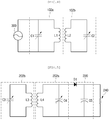
- FIG. 3 is an equivalent circuit diagram of a transfer induction coil according to an embodiment.
- the transmitting induction coil 102a may be configured of an inductor L1 and a capacitor C1, which may configure a circuit having a suitable inductance value and a suitable resistance value.
- the transmitting induction coil 102a may be configured with an equivalent circuit in which both ends of the inductor L1 are connected to both ends of the capacitor C1, respectively. That is, the transmitting induction coil 102a may be configured with an equivalent circuit in which the inductor L1 and the capacitor C1 are connected in parallel.
- the capacitor C1 may be a variable capacitor, so that an impedance matching is performed by controlling a capacitance of the capacitor C1.
- An equivalent circuit of the transmitting resonance coil 102b, the receiving resonance coil 202b and the receiving induction coil 202a may also be the same as or similar to that illustrated in FIG. 2 , which is not limited thereto.
- FIG. 4 is an equivalent circuit diagram of a power source and a wireless transfer device according to an embodiment.
- the transmitting induction coil 102a and the transmitting resonance coil 102b may be configured with the inductors L1 and L2 and the capacitors C1 and C2, respectively, the inductors and capacitors having their inductance values and capacitance values, respectively.
- FIG. 5 is an equivalent circuit diagram of a receiver according to an embodiment.
- the receiving resonance coil 202b and the receiving resonance coil 202a may be configured with inductors L3 and L4 and capacitors C3 and C4, respectively, the inductors and capacitors having their inductance values and capacitance values, respectively.
- the rectifying part 220 may convert an AC power transferred from the receiving inductance coil 202a into a DC power to transfer the converted DC power to the load 240.
- the rectifying part 220 may include a rectifier and a smoothing circuit, which are not illustrated.
- the rectifier may be a silicon rectifier that may be equalized with a diode D1 as illustrated in FIG. 5 , which is not limited thereto.
- the rectifier may convert an AC power transferred from the receiving induction coil 202a into a DC power.
- the smoothing circuit may remove an AC component included in the DC power converted in the rectifier and output a smooth DC power.
- the smoothing circuit may employ a rectifying capacitor C5 as illustrated in FIG. 5 , which is not limited thereto.
- a DC power transferred from the rectifying part 220 may be a DC voltage or a DC current, which is not limited thereto.
- the load 240 may be an arbitrary charger or device that needs a DC power.
- the load 240 may mean a battery.
- the receiving part 200 may be mounted on an electronic equipment that needs a power, such as a mobile phone, a laptop computer, a mouse, etc. Accordingly, the receiving resonance coil 202b and the receiving inductance coil 202a may have a shape adapted to that of the electronic equipment.
- the transmitting part 100 may exchange information using an in-band or out-of-band communication with the receiving part 200.
- the in-band communication may mean a communication scheme to exchange information between the transmitting part 100 and the receiving part 200 using signals having a frequency used for a wireless power transfer.
- the receiving part 200 may further include a switch, and may or may not receive the power transmitted from the wireless power transfer device 200 through a switching operation of the switch. Accordingly, the transmitting part 100 may detect the amount of power consumed in the transmitting part 100 to recognize an on or off signal of the switch included in the receiving part 200.
- the receiving part 200 may change the amount of power absorbed in a resistor element using the resistor element and a switch, capable of changing the amount of power consumed in the receiving part 200.
- the transmitting part 100 may sense changes of power consumed and obtain status information of the load 240.
- the switch and resistor element may be serially connected.
- the status information of the load 240 may include a current charging amount and a charging amount development of the load 240.
- the load 240 may be included in the receiving part 200.
- the switch when the switch is opened, the power absorbed by the resistor element becomes zero (0), and the power consumed in the receiving part 200 is also reduced.
- the transmitting part 100 may detect the power consumed in the transmitting part 100 and perform a digital communication with the receiving part 200.
- the transmitting part 100 may receive status information of the load 240 by the operations described above, and transmit a suitable power.
- the status information of the transmitting part 100 may include the maximum providing the amount of power that is transferred by the transmitting part 100, the number of the receiving parts 200 to which the transmitting part 100 provides the power, and available amount of power of the transmitting part 100.
- the out-of-band communication refers to a communication scheme in which information needed when transferring power is exchanged using a separate frequency band other than a resonance frequency band.
- An out-of-band communication module is mounted on both the transmitting part 100 and the receiving part 200, so that they may exchange information needed to transfer power.
- the out-of-band communication module may be mounted on the power source 300, which is not limited thereto.
- the out-of-band communication module may use a local area communication scheme such as blueTooth, Zigbee, wireless LAN and NFC, which is not limited thereto.
- FIG. 6 is a block diagram illustrating a transmitter of a wireless power transfer system according to an embodiment of the present disclosure
- FIG. 7 is a block diagram illustrating a receiver of a wireless power transfer system according to an embodiment of the present disclosure.
- the wireless power transfer system 10 may include a transmitting part 100 transmitting power in a wireless manner and a receiving part 200 receiving power from the transmitting part 100.
- the subsystem of the transmitting part 100 may include a transmitting power converter system 101 and a transfer antenna system 102.
- the transmitting power converter system 101 may include a number of subsystems, including a rectifying and filtering part 110, a converter 120, a power converting part 130, a control part 140 and a matching part 150.
- the rectifying and filtering part 110 generates a DC voltage to be used in the next stage, and the generated DC voltage is supplied to the converter 120 and then to the transmitting antenna system 102.
- the converter 120 together with the rectifying and filtering part 110 is configured of an AC/DC converter, which may rectify an AC voltage having a band of tens of Hz to generate a DC voltage.
- the converter 120 is configured independently from the rectifying and filtering part 110 to be a DC/DC converter that generates a DC voltage suitable to a power transfer. Also, the converter 120 may be a step-down converter to provide an output DC voltage that is lower than an input voltage, which is not limited thereto.
- the converter 120 may output a DC voltage whose voltage level is controlled by the control part 140.
- the power conversion part 130 may convert a DC voltage of a certain level into an AC voltage by a switching pulse signal of tens of KHz to tens of MHz, generating power. That is, the power conversion part 130 may convert a DC voltage into an AC voltage, generating a target, that is, "a wake-up voltage' or "a charging power” that is used in the receiving part 200 which is brought into a charging region.
- the wake-up power means a small power of 0.1 to 1mWatt
- the charging power is a power that is needed to charge a battery of the receiving part 200 or consumed when operating the receiving part 200, indicating a large power of 1mWatt to 200Watt consumed in a load of the target receiving part 200.
- the power conversion part 130 may include a power amplifier that amplifies a DC voltage according to a switching pulse signal.
- the power conversion part 130 may be configured of a full bridge inverter.
- the control part 140 may generate a frequency and a switching waveforms to drive the power conversion part 130 in consideration of the maximum power transfer efficiency, controlling the power to be transferred.
- the matching part 150 performs an impedance matching between the transmitting part 100 and the receiving part 200.
- the transmitting antenna system 102 may include at least one of the inductance coil 102a and the resonance coil 102b.
- the transmitting antenna system 102 may include the induction coil 102a only.
- the transmitting antenna system 102 may include the resonance coil 102b only.
- the transmitting antenna system 102 may include both the induction coil 102a and the resonance coil 102b.
- the induction coil 102a or the resonance coil 102b may be included in a single or in plural.
- the induction coil 102a or the resonance coil 102b may be disposed in an overlapping manner and an overlapping area may be determined in consideration of a deviation of magnetic flux.
- the receiving part 200 illustrated in FIG. 2 may include a receiving power converter system 201 and a receiving antenna system 202.
- the receiving antenna system 202 of the receiving part 200 may be the same as the transmitting antenna system 102, and dimensions of the receiving antenna may be changed depending on electrical characteristics of the receiving part 200.
- the receiving antenna system 202 may receive power in the magnetic induction scheme or magnetic resonance scheme.
- the receiving antenna system 202 may include at least one of the induction coil 202a and the resonance coil 202b depending on the power receiving scheme.
- the receiving antenna system 202 may further include a near field communication antenna.
- the receiving power converter system 201 may include a matching part 210, a rectifying part 220, a receiving side converter 230, a load 240 and a receiving side controller 250.
- the matching part 210 performs an impedance matching between the transmitter 100 and the receiver 200.
- the rectifying part 220 rectifies an AC voltage outputted from the receiving antenna system 202 to generate a DC voltage.
- the receiving side converter 230 may be configured of a DC/DC converter to control a level of the DC voltage outputted from the rectifying part 220 according to a load capacity.
- the load 240 may include a battery, a display device, a sound output circuit, a main processor and kinds of sensors.
- the receiving side control part 250 may be activated by a wake-up power from the transmitting part 100, perform a communication with the transmitting part 100, and control an operation of the subsystem of the receiving part 200.
- the receiving part 200 may be configured in a single or in plural, to simultaneously receive energy from the transmitting part 100 in a wireless manner. That is, in the wireless power transfer system employing the resonance scheme, a plurality of target receiving parts 200 may be supplied with power from one transmitting part 100.
- the matching part 150 of the transmitting part 100 may adaptively perform an impedance matching among a plurality of receiving parts 200.
- the receiving part 200 when configured in plural, they may become the same kind of system or different kinds of system.
- control part 140 of the transmitting part 100 may generally control the transmitting part 100.
- the control part 140 may control the power conversion part 130.
- the control part 140 may control the power conversion part 130 depending on statuses of the receiving part 200, that is, a charging status or a receiving status. For example, when the receiving part 200 requires a higher wireless power, the control part 140 may control the power conversion part 130 to generate a higher wireless power to be transmitted to the receiving part 200. For example, when the receiving part 200 requires a lower wireless power, the control part 140 controls the power conversion part 130 to generate a lower wireless power to be transmitted to the receiving part 200.
- the status of the receiving part 200 may be provided from the receiving part 200 in response to a request of the transmitting part 100. On the other hand, information on the status of the receiving part 200 may be provided to the transmitting part 100 arbitrarily or in a predetermined interval.
- the control part 140 may supply the power conversion part 130 with a PWM control signal whose duty ratio is controlled according to statuses of the receiving part 200 based on status information provided from the receiving part 200. Accordingly, the embodiment may regulate a control signal used to generate an AC power instead of regulating the magnitude of the power of the power source 300 or the output of the converter 120 in order to regulate an AC power to be transmitted to the receiving part 200 so as to change the magnitude of the AC power, preventing current from being lost and power from being wasted, thereby enhancing power transfer efficiency.
- FIG. 8 is a view illustrating a light device according to an embodiment.
- connection relationship and an operation method of the power conversion part 130 will be described with reference to FIG. 8 .
- the power conversion part 130 may convert power provided from the converter 120 into an AC power based on an AC power control signal provided from the control part 140 and amplify it. Also, the power conversion part 130 may include a full bridge inverter.
- the power conversion part 130 may include a first to a fourth switching elements S1, S2, S3 and S4.
- the first to fourth switching elements S1, S2, S3 and S4 each may conduct when a first to a fourth AC power control signals C11, C12, C21 and C22 provided from the control part 140 are in a high level, and open when in a low level.
- the first switching element S1 may be connected between a first node N1 and the converter 120, and controlled by a first AC power control signal C11 of the control part 140.
- the second switching element S2 may be connected between the first node N1 and a ground and controlled by a second AC power control signal C12 of the control part 140.
- the third switching element S3 may be connected between the second node N2 and the converter 120, and controlled by a third AC power control signal C21 of the control part 140.
- the fourth switching element S4 may be connected between the second node N2 and a ground, and controlled by a fourth AC power control signal C22 of the control part 140.
- the first to fourth switching elements S1, S2, S3 and S4 may be N-type MOSFET (Metal-Oxide-Semiconductor Field-Effect-Transistor), which is not limited thereto. Rather, elements that perform a switching operation by the AC power control signal of the control part 140 may be available.
- N-type MOSFET Metal-Oxide-Semiconductor Field-Effect-Transistor
- each gate terminal of the first to fourth switching elements S1, S2, S3 and S4 is applied an AC power control signal. Remaining two terminals of the first to fourth switching elements S1, S2, S3 and S4 may be source and drain terminals and current may flow from the drain terminal to the source terminal in the first to fourth switching elements S1, S2, S3 and S4.
- FIGS. 9 and 10 are views illustrating operations of a power conversion part
- FIG. 11 is a waveform view of an output signal of a power conversion part according to an AC power control signal.
- a positive polarity output voltage Vo may be applied to the matching part 150.
- a negative polarity output voltage Vo may be applied to the matching part 150.
- FIG. 11 shows the first to fourth AC power control signals C11, C12, C21 and C22 applied to the first to fourth switching elements S1, S2,S3 and S4 and a resultant output voltage Vo when a duty ratio is 50%, for example.
- a duty ratio 50%
- FIGS. 12 and 13 are views illustrating waveform diagrams to control a duty ratio of an AC voltage by controlling a blank interval.
- duty ratios of the first to fourth AC power control signals C11, C12, C21 and C22 that are PWM signals provided from the control part 140 may be changed. For example, rising times Tr11 Tr12, Tr21 and Tr22 and falling times Tf11, Tf12 Tf21 and Tf22 of high levels of the first to fourth AC power control signals C11, C12, C21 and C22 that are PWM signals provided from the control part 140 may be changed.
- the embodiment may enable the receiving part 200 to receive a constant power by differing a duty ratio Ton of the AC voltage Vo of the AC power depending on a status of the receiving part 200, for example, a charging status and/or a receiving status.
- the embodiment may interrupt the current that may be lost when an AC power is generated in the transmitting part 100, minimizing power consumption.
- FIG. 12 illustrates waveform diagrams of the first to fourth AC power control signals that are PWM signals to generate an AC power having an AC voltage of 50% duty ratio.
- the first to fourth AC power control signals C11, C12, C21 and C22 may be generated based on clock signals.
- the clock signal may be generated based on an AC signal of an oscillator (not illustrated) or by a separate means, which is not limited thereto.
- the clock signal (Clock) may be repeatedly generated in a cycle having a high level pulse and a low level pulse.
- the first AC power control signal C11 defines a rising time Tr11 for a high level at a time delayed for a predetermined time from a rising time of a first high level pulse in the clock signal (Clock) and a falling time Tf11 for a low level at a rising time of a second high level pulse.
- a high level section of the second AC power control signal C12 is not overlapped with a high level section of the first AC power control signal C11. If the high level section of the first AC power control signal C11 is overlapped with the high level section of the second AC power control signal C12, the first and second switching elements S1 and S2 are simultaneously conducted, an output voltage of the converter 120 is discharged to a ground, the output voltage of the converter 120 is not applied to the first node N1. As a result, power is not transferred to the transfer antenna system 102.
- a blank interval T PA may be defined where high level intervals of the first and second AC power control signals C11 and C12 do not exist between the falling time Tf11 of the first AC power control signal C11 and the rising time Tr12 of the second AC power control signal C12 or between the rising time Tr11 of the first AC power control signal C11 and the falling time Tf12 of the second AC power control signal C12.
- the second AC power control signal C12 may define a rising time Tr12 for a high level at a time delayed for a predetermined time from a rising time of a second high level in the clock signal (Clock) and a falling time Tf12 for a low level at a rising time of a third high level pulse.
- a high level interval of the third AC power control signal C21 may be partially overlapped with a high level interval of the first AC power control signal C11 and a high level interval of the second AC power control signal C12. That is, the rising time Tr21 of the third AC power control signal C21 is ahead of a falling time Tf11 of the first AC power control signal C11, and the falling time Tf21 of the third AC power control signal C21 follows the rising time Tr12 of the second AC power voltage signal C12.
- a high level interval of the fourth AC power control signal C22 is not overlapped with a high level interval of the third AC power control signal C21.
- the third and fourth switching elements S3 and S4 are simultaneously conducted, an output voltage of the converter 102 is discharged to a ground and the output voltage of the converter 120 is not applied to the second node N2. As a result, power is not transferred to the transfer antenna system 102.
- a blank interval T AP may be defined where high level intervals of the third and fourth AC power control signals C21 and C22 do not exist between a falling time Tf21 of the third AC power control signal C21 and a rising time Tr22 of the fourth AC power control signal C22 or between a rising time Tr21 of the third AC power control signal C21 and a falling time Tf22 of the fourth AC power control signal C22.
- the high level interval of the fourth AC power control signal C22 may be partially overlapped with the high level interval of the first AC power control signal C11 and a high level interval of the second AC power control signal C12. That is, the rising time Tr22 of the fourth AC power control signal C22 is ahead of a falling time Tf12 of the second AC power control signal C12, and follows the rising time Tr11 of the first AC power voltage signal C11.
- Respective high level intervals of the first to fourth AC power control signals C11, C12, C21 and C22 may be defined in a cycle of the clock signal (Clock).
- an high level overlapping interval of the first and fourth AC power control signals C11 and C22 is a power transfer interval, which may be defined as a duty ratio (Ton).
- the duty ratio (Ton) is an interval where a power may be transferred for a cycle, the maximum being set 50%, which is not limited thereto. For example, when a duty ratio is 50%, power can be transferred in a half cycle and cannot be transferred in the remaining half cycle.
- an overlapped high level interval of the second and third AC power control signals C12 and C21 is a power transfer available interval, which may be defined as a duty ratio (Ton).
- the duty ratio (Ton) is determined by the falling time Tf21 of the third AC power control signal C21 and the falling time Tf22 of the fourth AC power control signal C22.
- Ton the duty ratio
- the duty ratio Ton may be increased, and when the falling time is quickened, the duty ratio Ton may be decreased.
- the embodiment may reflect an increase or decrease of the AC power to be transferred to the receiving part 200 so that the control part 140 generates the first to fourth AC power control signals C11, C112, C21 and C22, a duty ratio (Ton) of an AC voltage (Vo) output from the power conversion part 130 may be regulated by the first to fourth AC power control signals C11, C12, C21 and C22, and the wireless power having an AC voltage (Vo) of the regulated duty ratio (Ton) may be transmitted to the receiving part 200 by the transmitting antenna system 102.
- a duty ratio (Ton) of an AC voltage (Vo) output from the power conversion part 130 may be regulated by the first to fourth AC power control signals C11, C12, C21 and C22
- the wireless power having an AC voltage (Vo) of the regulated duty ratio (Ton) may be transmitted to the receiving part 200 by the transmitting antenna system 102.
- FIG. 13 illustrates a waveform diagram of the first to fourth AC power control signals to generate an AC power having an AC voltage of 30% duty ratio.
- FIG. 13 a method for generating the first to fourth AC power control signals C11, C12, C21 and C22 is the same as that described with reference to FIG. 8 .
- An AC voltage (Vo) illustrate in FIG. 13 has a duty ratio (Ton) of 30%, which is smaller than the duty ratio (To) of 50% illustrated in FIG. 12 .
- Ton a duty ratio
- a width of a positive polarity voltage or a negative polarity voltage having a duty ratio (To) of 30% may be smaller than that of a positive polarity voltage or a negative polarity voltage having a duty ratio (To) of 50%.
- the first to fourth AC power control signals C11, C12, C21 and C22 may be changed so that the duty ratio of the AC voltage (Vo) may be reduced to 30%. That is, the falling time Tf12 of the second AC power control signal C12 and the falling time Tf21 of the third AC power control signal C21 illustrated in FIG. 13 may be ahead of the falling time Tf12 of the second AC power control signal C12 and the falling time Tf21 of the third AC power control signal C21 illustrated in FIG. 12 . Accordingly, as the duty ratio (Ton) of the AC voltage Vo is reduced, the falling time Tf12 of the second AC power control signal C12 and the falling time Tf21 of the third AC power control signal C21 may be quickened more and more. For example, the falling time Tf12 of the second AC power control signal C12 and the falling time Tf21 of the third AC power control signal C21 may be more quickened in a duty ratio (Ton) of 20% rather than a duty ratio (Ton) of 30%.
- control part 140 may include a fist serve control part that generates the first to fourth AC power control signals C11 to C22 that are PWM signals, to be provided to the first to fourth switching elements S1 to S4 and a second serve control part that provides the first serve control part with a duty ratio regulation signal to regulate duty ratios of the first to fourth AC power control signals C11 to C22.
- the second serve control part may supply the first serve control part with a duty ratio regulation signal regulated depending on a status of the receiving part 200 based on status information provided from the receiving part 200.
- the duty ratio regulation signal may be a binary data of 6 bits.
- the first serve control part may generate the first to fourth AC power control signals C11 to C22 to generate an AC power having an AC voltage of a duty ratio of 50% in response to the duty ratio regulation.
- the AC power having the AC voltage of a duty ratio of 50% may be the maximum AC power to be transmitted to the receiving part 200, which is not limited4d thereto.
- the first serve control part may generate the first to fourth AC power control signals C11 to C22 to generate an AC power having an AC voltage of a duty ratio of 40% in response to the control signal.
- the first serve control part may generate the first to fourth AC power control signals C11 to C22 to generate an AC power having an AC voltage of a duty ratio of 30% in response to the control signal.
- the first serve control part may generate the first to fourth AC power control signals C11 to C22 to generate an AC power having an AC voltage of a duty ratio of 20% in response to the control signal.
- the first serve control part may generate the first to fourth AC power control signals C11 to C22 to generate an AC power having an AC voltage of a duty ratio of 10% in response to the control signal.
- the first to fourth AC power control signals C11 to C22 to generate an AC power in a duty ratio unit of 5%, a duty ratio unit of 3%, or a duty ratio unit of 2%, which is not limited thereto.
- FIGS. 14A, 14B, 15A , 15C , 16A and 16B are views illustrating the magnitude of a fundamental wave of a signal outputted as a result of simulating an output waveform when changing a duty ratio of a full bridge of a power converter and the magnitude of a harmonic that is multiple components of a fundamental wave.
- a simulation is performed using a Fourier analysis of an output signal, basically.
- a total harmonics distortion THD is used in order to compare degrees of harmonic components depending on duty ratios.
- the total harmonics distortion THD is defined as a ratio of an RMS of a harmonic component and an RMS of a fundamental wave, which indicates degrees of harmonic occurrence.
- the total harmonics distortion THD is defined as a maximum harmonics distortion that is a ratio of an RMS of a maximum magnitude harmonic component having the maximum magnitude of harmonic components and an RMS of a fundamental wave. That is, the maximum harmonic distortion is defined as a ratio of an RMS of a maximum magnitude harmonic component contrasted with an RMS of a fundamental wave.
- a simulation result is produced by changing a duty ratio to 50%, 40% and 30% based on an amplitude of an output waveform 1V and a cycle, 143Hz.
- a fundamental wave has a value of about 0.6V, and even number and even number harmonics appear and the magnitude of a first harmonic component which is twice of a fundamental frequency among harmonic components is between 0.1V and 0.2V.
- FIGS. 16A and 15b illustrate a case that a duty ratio is 30%.
- a fundamental wave has a magnitude between 0.5V and 0.6V
- FIG. 17 is a view illustrating a simulation result of the maximum harmonic distortion ratio when changing a duty ratio.
- the maximum harmonic distortion has a relatively small value in a duty ration interval of 0.26 to 0.44 (26% to 44%). That is, the duty ratio interval is an interval where less harmonic components are distributed.
- the maximum harmonic distortion is smallest when a duty ratio is 0.41(41%) and 0.32(32%), and the value of the maximum harmonic distortion becomes 23.6%.
- a perfect sine wave does not include harmonic components
- a sine wave having a distorted waveform due to a non-linear characteristic of a load includes harmonic components. Accordingly, when controlling an output voltage Vo to be approximated to a sine wave, the harmonic components may be reduced and an electromagnetic compatibility EMC may be maximized.
- the above-described simulation reviews an EMC characteristic using a ratio of the magnitude of a fundamental wave and the magnitude of the maximum harmonic component, which is not limited thereto. Rather, the EMC characteristic may be considered using a ratio of the magnitude of a fundamental wave and the magnitude of total harmonic components.
- FIG. 18 is a signal flow chart illustrating operations of a wireless power transfer system according to an embodiment of the present disclosure.
- a first step is a sensing step (S100).
- a wireless power transfer may start when the transmitting part 100 senses the receiving part 200 or in reverse the receiving part 200 senses the transmitting part 100.
- the sensing step (S100) may be configured of substeps, a selection step to sense the receiving part 200, a ping step to receive a packet, and an identification and configuration step to receive a unique ID, an extension ID, and information on control parameters.
- a second step is a power requesting step (S200).
- the receiving part 200 requests the transmitting part 100 to transmit power
- the receiving part 200 may request the transmitting part 100 to transmit a certain amount of power depending on status of the receiving part 200, that is, battery charging status of the receiving part 200, temperature status of the receiving part 200 and battery, the amount and degree of battery power consumption and battery charging speed.
- a third step is a step to control the control part 140 and the converter 120 (S300).
- the power transmission amount may be changed depending on status of the receiving part 200, and accordingly the control part 140 of the transmitting part 100 may control the converter 120 to regulate level of the DC power.
- a fourth step is a step to control the power conversion part 130 of the control part 140 (S400) and a step to transmit power (S500).
- the converter 120 may control first to fourth switching elements S1, S2, S3 and S4 of a full bridge inverter inside the power conversion part 130 using a PWM control signal.
- a turning on or off ratio of the first to fourth switching elements S1, S2, S3 and S4 may be changed according to a duty ratio, and a degree of the harmonic components included in the power conversion part 130 may be changed according to a duty ratio.
- the control part may analyze the magnitude of the DC voltage transferred to the power conversion part 130 from the converter 120 and a frequency component of the output signal outputted from the power conversion part 130 to control a duty ratio of the PWM control signal.
- control part 140 may determine a duty ratio to have a predetermined value among 26% to 44%, for example and provide the power conversion part 130 with a PWM control signal having the predetermined value as well. Also, the control part 140 may be fed back with signals outputted from the power conversion part 130, analyze harmonic components of the output signal to provide the power conversion part 130 with PWM control signal having a duty ratio in which a ratio of the magnitude of a fundamental wave and the magnitude of a maximum harmonic is a minimum, so that the control part 140 may enable the transmitting part 100 to provide the power requested by the receiving part 200.
- the output signal of the power conversion part 130 may be fed back and analyzed each predetermined period. Therefore, a real time control may be performed to determine a distortion degree of the power conversion part 130 depending on changes of the power transmission condition of the wireless power transfer system 10 or changes of system characteristic to output output signals having optimized electromagnetic characteristic.
- the transmitting part 100 of the wireless power transfer system 10 uses a full bridge inverter as the power converter 130.
- the full bridge inverter has an effect to approximate the output signal to a sine wave so that the harmonic components are minimized, as well as an effect to increase the maximum power provided to the transmitting antenna system 102 compared with an half bridge inverter in the art.
- control part 140 may regulate a duty ratio of the DC voltage level outputted from the converter 120 and first to fourth AC power control signals C11, C12, C21 and C22 that are PWM control signals provided to the power conversion part 130 to reduce harmonic components of the output signals outputted from the power conversion part 130. Also, the control part 140 may be fed back with the amount of power requested in the receiving part 200 and distortion status of the output signal of the power conversion part 130 depending on current status of the transmitting part and receiving part 100 and 200 to regulate a duty ratio of the first to fourth power control signals C11, C12, C21 and C22, thereby improving electromagnetic wave characteristics.
- the method according to the above-described embodiment may be manufactured with a computer executable program and stored in a computer readable recording medium.
- the computer-readable recording medium include a ROM, RAM, CD-ROM, magnetic tape, floppy disk, optical data storage device and so on. Also, it may be implemented in the form of a carrier wave (e.g., transmission over Internet).
- the computer-readable recording medium may be distributed in the computer system connected through a computer communication network, and may be stored and executed as codes readable in a distributed manner.
- functional program, code and code segments, used to implement the present disclosure can be derived by a skilled computer programmer from the description of the disclosure contained herein.
- the receiving part 200 may be mounted on a mobile terminal such as a mobile phone, a smart phone, a laptop computer, a digital broadcasting terminal, a personal digital assistance PDA, a portable multimedia player PMP, a navigation, and so on.
- a mobile terminal such as a mobile phone, a smart phone, a laptop computer, a digital broadcasting terminal, a personal digital assistance PDA, a portable multimedia player PMP, a navigation, and so on.
- the configuration of the embodiment may also be applicable to stationary terminals such as digital TV, desktop computer and the like, except the case applicable to mobile terminal only.
- the power transmission scheme by electromagnetic induction may mean a relatively low Q value and a tight coupling
- the power transmission scheme by resonance may mean a relatively high Q value and a loose coupling
- the wireless power transfer device may be used in the field of wireless charging system.
Landscapes
- Engineering & Computer Science (AREA)
- Computer Networks & Wireless Communication (AREA)
- Power Engineering (AREA)
- Signal Processing (AREA)
- Charge And Discharge Circuits For Batteries Or The Like (AREA)
- Inverter Devices (AREA)
Claims (12)
- Ein Sender (100) zum Erzeugen einer drahtlosen Energie, die zu einem Empfänger (200) zu übertragen ist, wobei der Sender (100) umfasst:ein Leistungswandlerteil (130) mit einem Vollbrücken-Inverter; undeinem Steuerteil (140) zur Steuerung des Leistungswandlerteils (130) unter Verwendung von PWM-Steuersignalen (Pulsweitenmodulation),dadurch gekennzeichnet, dass das Steuerteil (140) so konfiguriert ist, dass es ein Tastverhältnis des PWM-Steuersignals durch ein Tastverhältnis bestimmt, bei dem die maximale harmonische Verzerrung eines Ausgangssignals des Leistungswandlerteils (130) einen minimalen Wert hat,wobei die maximale harmonische Verzerrung als ein Verhältnis eines RMS einer harmonischen Komponente maximaler Größe definiert ist, die einem RMS einer Grundwelle entgegengesetzt ist.
- Der Sender (100) nach Anspruch 1, wobei das Tastverhältnis 26% bis 44% beträgt.
- Der Sender (100) nach Anspruch 1, wobei das Tastverhältnis 41% oder 32% beträgt.
- Der Sender (100) nach Anspruch 1, weiter umfassend:ein Gleichrichter- und Filterteil (110), das so konfiguriert ist, dass es eine AC-Eingangsleistung empfängt und eine Gleichspannung erzeugt;einen DC/DC-Wandler zum Regeln eines Pegels der Gleichspannung, die von dem Gleichrichtungs- und Filterteil (110) ausgegeben wird, um an den Leistungswandlerteil (130) ausgegeben zu werden; undein Anpassungsteil zur Durchführung einer Impedanzanpassung zwischen dem Sender (100) und dem Empfänger (200),wobei der Steuerteil (140) einen Gleichspannungspegel des DC/DC-Wandlers steuert.
- Ein Verfahren zum Ansteuern eines drahtlosen Leistungsübertragungssystems, das einen Sender (100) mit einem Leistungswandlerteil (130) zum Umwandeln von Leistung, die von einer externen Leistungsversorgung zugeführt wird, und einen Empfänger (200) zum Empfangen von Leistung von dem Sender (100) enthält, wobei das Verfahren umfasst:Ermöglichen, dass, wenn sich der Empfänger (200) einem Ladebereich des Senders (100) nähert, entweder der Sender (100) oder der Empfänger (200) den anderen erfasst;Ermöglichen, dass der Empfänger (200) den Sender (100) auffordert, Leistung zu übertragen;Ermöglichen, dass ein Steuerteil (140) des Senders (100) einen Gleichspannungspegel des DC/DC-Wandlers in Abhängigkeit von der vom Empfänger (200) angeforderten Leistungsmenge reguliert; undermöglichen dem Steuerteil (140) die Steuerung des Leistungsumwandlungsteils (130) in Abhängigkeit von einem Tastverhältnis von vorbestimmten PWM-Steuersignalen zu steuern, dadurch gekennzeichnet, dass das Tastverhältnis des PWM-Steuersignals durch ein Tastverhältnis bestimmt wird, bei dem die maximale harmonische Verzerrung eines Ausgangssignals des Leistungswandlerteils (130) einen minimalen Wert hat,wobei die maximale harmonische Verzerrung als ein Verhältnis eines RMS einer harmonischen Komponente maximaler Größe definiert ist, die einem RMS einer Grundwelle entgegengesetzt ist.
- Verfahren nach Anspruch 5, wobei der Leistungswandlerteil (130) einen Vollbrücken-Inverter enthält, der eine Gleichspannung von einem DC/DC-Wandler erhält, um ein AC-Signal auszugeben.
- Verfahren nach Anspruch 5, wobei das Tastverhältnis 26% bis 44% beträgt.
- Verfahren nach Anspruch 5, wobei das Tastverhältnis 41% oder 32% beträgt.
- Verfahren nach Anspruch 5, bei dem das Steuerteil (140) mit einem von dem Leistungswandlerteil (130) ausgegebenen Ausgangssignal rückgekoppelt wird und das Leistungswandlerteil (130) mit einem PWM-Steuersignal mit einem Tastverhältnis versorgt, bei dem das Verhältnis der Größe einer Harmonischen zur Größe einer Grundfrequenz des Ausgangssignals ein Minimum ist.
- Sender (100) nach Anspruch 1, wobei der Sender (100) umfasst:das Steuerteil (140) zum Erzeugen eines ersten bis vierten Wechselstrom-Leistungssteuersignals; undden Leistungswandlerteil (130) zum Erzeugen einer Wechselstromleistung einschließlich einer Elektrodenspannung positiver Polarität und einer Elektrodenspannung negativer Polarität als Reaktion auf das erste bis vierte Wechselstrom-Leistungssteuersignal,wobei das Leistungswandlerteil (130) die Elektrodenspannung positiver Polarität als Reaktion auf das erste und vierte Wechselstrom-Leistungssteuersignal und die Elektrodenspannung negativer Polarität als Reaktion auf das zweite und dritte Wechselstrom-Leistungssteuersignal erzeugt.
- Sender (100) nach Anspruch 10, wobei das Tastverhältnis in Abhängigkeit von einem Leistungsempfangsstatus des Empfängers (200) geregelt wird.
- Sender nach Anspruch 11, wobei die Abfallzeit des vierten Wechselstrom-Leistungssteuersignals vor der Abfallzeit des ersten Wechselstrom-Leistungssteuersignals liegt.
Applications Claiming Priority (3)
| Application Number | Priority Date | Filing Date | Title |
|---|---|---|---|
| KR1020140002327A KR102146484B1 (ko) | 2014-01-08 | 2014-01-08 | 전력 생성 장치, 무선 전력 송신 장치 및 무선 전력 전송 시스템 |
| KR1020140009243A KR102175599B1 (ko) | 2014-01-24 | 2014-01-24 | 무선전력전송 시스템 |
| PCT/KR2015/000163 WO2015105334A1 (ko) | 2014-01-08 | 2015-01-07 | 무선 전력 송신 장치 및 무선 전력 전송 시스템 |
Publications (3)
| Publication Number | Publication Date |
|---|---|
| EP3096437A1 EP3096437A1 (de) | 2016-11-23 |
| EP3096437A4 EP3096437A4 (de) | 2017-11-01 |
| EP3096437B1 true EP3096437B1 (de) | 2020-11-04 |
Family
ID=53524111
Family Applications (1)
| Application Number | Title | Priority Date | Filing Date |
|---|---|---|---|
| EP15734986.1A Not-in-force EP3096437B1 (de) | 2014-01-08 | 2015-01-07 | Vorrichtung zur drahtlosen stromübertragung und verfahren zur drahtlosen stromübertragung |
Country Status (5)
| Country | Link |
|---|---|
| US (1) | US10193392B2 (de) |
| EP (1) | EP3096437B1 (de) |
| JP (1) | JP6353545B2 (de) |
| CN (1) | CN106063080A (de) |
| WO (1) | WO2015105334A1 (de) |
Families Citing this family (23)
| Publication number | Priority date | Publication date | Assignee | Title |
|---|---|---|---|---|
| JP6302549B2 (ja) * | 2014-06-13 | 2018-03-28 | 株式会社東芝 | インダクタユニット、無線電力伝送装置、及び電動車両 |
| KR101775234B1 (ko) * | 2015-10-16 | 2017-09-05 | 엘지이노텍 주식회사 | 무전전력전송 시스템 및 이의 구동 방법. |
| KR102572577B1 (ko) * | 2016-04-15 | 2023-08-30 | 삼성전자주식회사 | 무선 충전을 제어하는 충전 장치 및 방법 |
| KR102588613B1 (ko) * | 2016-05-13 | 2023-10-11 | 엘지이노텍 주식회사 | 무선 충전 방법 및 그를 위한 장치 및 시스템 |
| CN106451818B (zh) * | 2016-10-25 | 2018-12-11 | 哈尔滨工业大学 | 基于磁耦合谐振的轮毂电机无线供电系统 |
| KR102602386B1 (ko) * | 2016-11-29 | 2023-11-16 | 삼성전자주식회사 | 무선 충전 방법 및 이를 지원하는 전자 장치 |
| CN106549457B (zh) * | 2016-12-27 | 2019-01-11 | 深圳大学 | 一种无线充电驱动芯片 |
| US10974608B2 (en) * | 2017-07-19 | 2021-04-13 | Hyundai Motor Company | Method and apparatus for selectively performing full bridge control and half bridge control in wireless power transfer system using LCCL-S resonant network |
| US11196298B2 (en) * | 2018-03-28 | 2021-12-07 | Apple Inc. | Wireless charging device with sinusoidal pulse-width modulation |
| US12105525B2 (en) * | 2018-09-06 | 2024-10-01 | The Trustees Of Indiana University | Caravanning autonomous vehicles |
| AU2018247282B2 (en) * | 2018-10-11 | 2025-08-14 | Aristocrat Technologies Australia Pty Limited | System and method for determining wireless charging status |
| KR102702930B1 (ko) * | 2018-10-22 | 2024-09-05 | 엘지이노텍 주식회사 | 무선 전력 제어 방법 및 장치 |
| WO2021035614A1 (zh) * | 2019-08-29 | 2021-03-04 | 深圳市大疆创新科技有限公司 | 驱动电路、驱动电路板与驱动器 |
| CN113098152B (zh) | 2020-01-08 | 2025-07-25 | 北京小米移动软件有限公司 | 无线充电方法及装置、折叠屏电子设备、存储介质 |
| CZ310061B6 (cs) * | 2020-01-29 | 2024-07-03 | MEGAHERTZ s.r.o. | Zařízení, zejména pro bezdrátové napájení a nabíjení |
| CN115428297A (zh) * | 2020-03-05 | 2022-12-02 | 扬科技术有限公司 | 汽车座椅无线充电系统 |
| CN114114111B (zh) * | 2020-08-26 | 2024-02-20 | 西门子(深圳)磁共振有限公司 | 一种局部线圈、磁共振成像系统的功率控制系统和方法 |
| KR102863897B1 (ko) | 2020-09-29 | 2025-09-25 | 삼성전자 주식회사 | 무선 충전 시스템을 위한 새로운 pwm 방식 |
| WO2022074479A1 (en) * | 2020-10-09 | 2022-04-14 | Cochlear Limited | Quantized waveform power transmission |
| EP4298868B1 (de) * | 2021-02-25 | 2025-01-01 | Signify Holding B.V. | Leuchte mit drahtloser resonanzkopplung |
| US11595027B2 (en) * | 2021-03-01 | 2023-02-28 | Nxp Usa, Inc. | High frequency pulse width modulation shaping |
| CN114709938B (zh) * | 2022-02-17 | 2025-01-28 | 河北工业大学 | 一种适用于无线电能传输系统的倍频控制策略 |
| CN119651933B (zh) * | 2025-02-18 | 2025-08-05 | 华东交通大学 | 一种基于变拓扑双向ac/ac的双向wpt交交变频系统 |
Family Cites Families (20)
| Publication number | Priority date | Publication date | Assignee | Title |
|---|---|---|---|---|
| JPH11224822A (ja) * | 1998-02-04 | 1999-08-17 | Hitachi Kiden Kogyo Ltd | 非接触給電装置における高調波電流抑制方法 |
| US7091762B2 (en) | 2001-10-09 | 2006-08-15 | Gallitzin Allegheny Llc | Systems and methods for minimizing harmonic interference |
| US9491638B2 (en) | 2005-03-09 | 2016-11-08 | Xirrus, Inc. | Wireless access point array |
| US8278784B2 (en) | 2008-07-28 | 2012-10-02 | Qualcomm Incorporated | Wireless power transmission for electronic devices |
| KR101705735B1 (ko) | 2010-04-08 | 2017-02-10 | 삼성전자주식회사 | 공진 전력 발생 장치 |
| CN102593957A (zh) * | 2011-01-18 | 2012-07-18 | 深圳市博巨兴实业发展有限公司 | 一种无线充电发射端、接收端和无线充电装置 |
| CN102222967B (zh) * | 2011-06-17 | 2013-09-18 | 武汉中原电子集团有限公司 | 一种自适应无线充电系统 |
| US9257910B2 (en) * | 2011-07-07 | 2016-02-09 | Danmarks Tekniske Universitet | Isolated boost flyback power converter |
| JP5545415B2 (ja) * | 2011-09-07 | 2014-07-09 | 株式会社村田製作所 | 電力伝送システムおよび送電装置 |
| JP5794056B2 (ja) | 2011-09-12 | 2015-10-14 | ソニー株式会社 | 給電装置および給電システム |
| JP2013106490A (ja) * | 2011-11-16 | 2013-05-30 | Advantest Corp | ワイヤレス給電装置およびワイヤレス給電システムならびに電力信号の送信方法 |
| US9088222B2 (en) | 2011-11-17 | 2015-07-21 | Qualcomm Incorporated | Systems, methods, and apparatus for a high power factor single phase rectifier |
| US9225391B2 (en) * | 2012-03-19 | 2015-12-29 | Lg Innotek Co., Ltd. | Wireless power transmitting apparatus and method thereof |
| CN102611215B (zh) * | 2012-04-10 | 2015-11-25 | 海尔集团公司 | 无线电能发射装置及无线充电系统 |
| JP2013223409A (ja) * | 2012-04-19 | 2013-10-28 | Sony Corp | 送電装置、非接触電力伝送システムおよび信号生成方法 |
| JP5906946B2 (ja) * | 2012-05-31 | 2016-04-20 | 日産自動車株式会社 | 非接触給電装置 |
| CN102751773A (zh) * | 2012-07-10 | 2012-10-24 | 上海市电力公司 | 一种用于电动汽车的无线充电系统 |
| US9859956B2 (en) * | 2012-08-24 | 2018-01-02 | Qualcomm Incorporated | Power supply control in wireless power transfer systems |
| TWI465027B (zh) * | 2012-09-19 | 2014-12-11 | Ind Tech Res Inst | 全橋式準諧振直流-直流轉換器及其驅動方法 |
| TWI473382B (zh) * | 2012-09-28 | 2015-02-11 | Au Optronics Corp | 無線電力傳輸裝置 |
-
2015
- 2015-01-07 WO PCT/KR2015/000163 patent/WO2015105334A1/ko not_active Ceased
- 2015-01-07 JP JP2016545862A patent/JP6353545B2/ja not_active Expired - Fee Related
- 2015-01-07 CN CN201580012340.9A patent/CN106063080A/zh active Pending
- 2015-01-07 US US15/110,665 patent/US10193392B2/en active Active
- 2015-01-07 EP EP15734986.1A patent/EP3096437B1/de not_active Not-in-force
Non-Patent Citations (1)
| Title |
|---|
| None * |
Also Published As
| Publication number | Publication date |
|---|---|
| US20160329752A1 (en) | 2016-11-10 |
| WO2015105334A1 (ko) | 2015-07-16 |
| JP2017504298A (ja) | 2017-02-02 |
| EP3096437A4 (de) | 2017-11-01 |
| CN106063080A (zh) | 2016-10-26 |
| JP6353545B2 (ja) | 2018-07-04 |
| EP3096437A1 (de) | 2016-11-23 |
| US10193392B2 (en) | 2019-01-29 |
Similar Documents
| Publication | Publication Date | Title |
|---|---|---|
| US10193392B2 (en) | Wireless power transfer device and wireless power transfer system | |
| US10141769B2 (en) | Wireless power transfer system | |
| US10566825B2 (en) | Wireless power transfer system having wireless power transfer system-charger | |
| EP2824799A1 (de) | Kraftübertragungssystem | |
| US10097029B2 (en) | Wireless charging transmitter | |
| US20150249483A1 (en) | Wireless power transmission system | |
| US9773609B2 (en) | Power supply apparatus and power control method thereof | |
| KR102175599B1 (ko) | 무선전력전송 시스템 | |
| US9148024B2 (en) | Apparatuses, systems, and methods for a monotonic transfer function in wireless power transfer systems | |
| EP4358363B1 (de) | Stromempfangsvorrichtung, stromsendevorrichtung und stromübertragungsverfahren | |
| CN106655528B (zh) | 基于双侧lc网络的ecpt系统及其参数设计方法 | |
| EP2722966A1 (de) | Kontaktloses energieversorgungssystem | |
| EP3334006A1 (de) | System zur drahtlosen energieübertragung und betriebsverfahren dafür | |
| Boscaino et al. | A wireless battery charger architecture for consumer electronics | |
| JP2018007462A (ja) | 非接触電力伝送システム | |
| US9899874B2 (en) | Electric power supplying device, of a wireless electric power transmission apparatus and method for supplying electric power | |
| KR20150115339A (ko) | 무선전력전송 시스템 | |
| KR102713285B1 (ko) | 무선 전력 송신 장치 및 이를 포함하는 무선 전력 송수신 시스템 | |
| US11469724B2 (en) | Free-boost class-e amplifier | |
| EP3876389A1 (de) | Dynamische resonanz für drahtlose stromsysteme | |
| KR102146484B1 (ko) | 전력 생성 장치, 무선 전력 송신 장치 및 무선 전력 전송 시스템 | |
| KR20150112160A (ko) | 무선전력전송 송신 장치를 구비한 무선전력전송 시스템 | |
| EP4318871A1 (de) | Verfahren und vorrichtung zum drahtlosen laden | |
| KR20240038527A (ko) | 무선 전력 송신 장치 및 그 동작 방법 |
Legal Events
| Date | Code | Title | Description |
|---|---|---|---|
| PUAI | Public reference made under article 153(3) epc to a published international application that has entered the european phase |
Free format text: ORIGINAL CODE: 0009012 |
|
| 17P | Request for examination filed |
Effective date: 20160707 |
|
| AK | Designated contracting states |
Kind code of ref document: A1 Designated state(s): AL AT BE BG CH CY CZ DE DK EE ES FI FR GB GR HR HU IE IS IT LI LT LU LV MC MK MT NL NO PL PT RO RS SE SI SK SM TR |
|
| AX | Request for extension of the european patent |
Extension state: BA ME |
|
| RIN1 | Information on inventor provided before grant (corrected) |
Inventor name: BAE, SU HO |
|
| DAX | Request for extension of the european patent (deleted) | ||
| RAP1 | Party data changed (applicant data changed or rights of an application transferred) |
Owner name: LG INNOTEK CO., LTD. |
|
| A4 | Supplementary search report drawn up and despatched |
Effective date: 20171005 |
|
| RIC1 | Information provided on ipc code assigned before grant |
Ipc: H02J 50/00 20160101ALI20170925BHEP Ipc: H02J 50/12 20160101AFI20170925BHEP Ipc: H02J 7/02 20160101ALI20170925BHEP Ipc: H04B 5/00 20060101ALI20170925BHEP Ipc: H02J 50/80 20160101ALN20170925BHEP Ipc: H02J 7/00 20060101ALI20170925BHEP |
|
| STAA | Information on the status of an ep patent application or granted ep patent |
Free format text: STATUS: EXAMINATION IS IN PROGRESS |
|
| 17Q | First examination report despatched |
Effective date: 20190916 |
|
| REG | Reference to a national code |
Ref country code: DE Ref legal event code: R079 Ref document number: 602015061488 Country of ref document: DE Free format text: PREVIOUS MAIN CLASS: H02J0050000000 Ipc: H02J0050120000 |
|
| GRAP | Despatch of communication of intention to grant a patent |
Free format text: ORIGINAL CODE: EPIDOSNIGR1 |
|
| STAA | Information on the status of an ep patent application or granted ep patent |
Free format text: STATUS: GRANT OF PATENT IS INTENDED |
|
| RIC1 | Information provided on ipc code assigned before grant |
Ipc: H04B 5/00 20060101ALI20200415BHEP Ipc: H02J 7/00 20060101ALI20200415BHEP Ipc: H02J 7/02 20160101ALI20200415BHEP Ipc: H02J 50/12 20160101AFI20200415BHEP Ipc: H02J 50/00 20160101ALI20200415BHEP Ipc: H02J 50/80 20160101ALI20200415BHEP |
|
| INTG | Intention to grant announced |
Effective date: 20200514 |
|
| GRAS | Grant fee paid |
Free format text: ORIGINAL CODE: EPIDOSNIGR3 |
|
| GRAA | (expected) grant |
Free format text: ORIGINAL CODE: 0009210 |
|
| STAA | Information on the status of an ep patent application or granted ep patent |
Free format text: STATUS: THE PATENT HAS BEEN GRANTED |
|
| AK | Designated contracting states |
Kind code of ref document: B1 Designated state(s): AL AT BE BG CH CY CZ DE DK EE ES FI FR GB GR HR HU IE IS IT LI LT LU LV MC MK MT NL NO PL PT RO RS SE SI SK SM TR |
|
| REG | Reference to a national code |
Ref country code: GB Ref legal event code: FG4D |
|
| REG | Reference to a national code |
Ref country code: CH Ref legal event code: EP |
|
| REG | Reference to a national code |
Ref country code: AT Ref legal event code: REF Ref document number: 1332092 Country of ref document: AT Kind code of ref document: T Effective date: 20201115 |
|
| REG | Reference to a national code |
Ref country code: IE Ref legal event code: FG4D |
|
| REG | Reference to a national code |
Ref country code: DE Ref legal event code: R096 Ref document number: 602015061488 Country of ref document: DE |
|
| REG | Reference to a national code |
Ref country code: NL Ref legal event code: MP Effective date: 20201104 |
|
| REG | Reference to a national code |
Ref country code: AT Ref legal event code: MK05 Ref document number: 1332092 Country of ref document: AT Kind code of ref document: T Effective date: 20201104 |
|
| PG25 | Lapsed in a contracting state [announced via postgrant information from national office to epo] |
Ref country code: GR Free format text: LAPSE BECAUSE OF FAILURE TO SUBMIT A TRANSLATION OF THE DESCRIPTION OR TO PAY THE FEE WITHIN THE PRESCRIBED TIME-LIMIT Effective date: 20210205 Ref country code: PT Free format text: LAPSE BECAUSE OF FAILURE TO SUBMIT A TRANSLATION OF THE DESCRIPTION OR TO PAY THE FEE WITHIN THE PRESCRIBED TIME-LIMIT Effective date: 20210304 Ref country code: RS Free format text: LAPSE BECAUSE OF FAILURE TO SUBMIT A TRANSLATION OF THE DESCRIPTION OR TO PAY THE FEE WITHIN THE PRESCRIBED TIME-LIMIT Effective date: 20201104 Ref country code: FI Free format text: LAPSE BECAUSE OF FAILURE TO SUBMIT A TRANSLATION OF THE DESCRIPTION OR TO PAY THE FEE WITHIN THE PRESCRIBED TIME-LIMIT Effective date: 20201104 Ref country code: NO Free format text: LAPSE BECAUSE OF FAILURE TO SUBMIT A TRANSLATION OF THE DESCRIPTION OR TO PAY THE FEE WITHIN THE PRESCRIBED TIME-LIMIT Effective date: 20210204 |
|
| REG | Reference to a national code |
Ref country code: DE Ref legal event code: R082 Ref document number: 602015061488 Country of ref document: DE Representative=s name: PETERREINS SCHLEY PATENT- UND RECHTSANWAELTE P, DE |
|
| REG | Reference to a national code |
Ref country code: DE Ref legal event code: R082 Ref document number: 602015061488 Country of ref document: DE Representative=s name: PETERREINS SCHLEY PATENT- UND RECHTSANWAELTE P, DE Ref country code: DE Ref legal event code: R081 Ref document number: 602015061488 Country of ref document: DE Owner name: SCRAMOGE TECHNOLOGY LIMITED, IE Free format text: FORMER OWNER: LG INNOTEK CO., LTD., SEOUL, KR Ref country code: DE Ref legal event code: R081 Ref document number: 602015061488 Country of ref document: DE Owner name: NERA INNOVATIONS LTD., IE Free format text: FORMER OWNER: LG INNOTEK CO., LTD., SEOUL, KR |
|
| PG25 | Lapsed in a contracting state [announced via postgrant information from national office to epo] |
Ref country code: SE Free format text: LAPSE BECAUSE OF FAILURE TO SUBMIT A TRANSLATION OF THE DESCRIPTION OR TO PAY THE FEE WITHIN THE PRESCRIBED TIME-LIMIT Effective date: 20201104 Ref country code: IS Free format text: LAPSE BECAUSE OF FAILURE TO SUBMIT A TRANSLATION OF THE DESCRIPTION OR TO PAY THE FEE WITHIN THE PRESCRIBED TIME-LIMIT Effective date: 20210304 Ref country code: LV Free format text: LAPSE BECAUSE OF FAILURE TO SUBMIT A TRANSLATION OF THE DESCRIPTION OR TO PAY THE FEE WITHIN THE PRESCRIBED TIME-LIMIT Effective date: 20201104 Ref country code: PL Free format text: LAPSE BECAUSE OF FAILURE TO SUBMIT A TRANSLATION OF THE DESCRIPTION OR TO PAY THE FEE WITHIN THE PRESCRIBED TIME-LIMIT Effective date: 20201104 Ref country code: AT Free format text: LAPSE BECAUSE OF FAILURE TO SUBMIT A TRANSLATION OF THE DESCRIPTION OR TO PAY THE FEE WITHIN THE PRESCRIBED TIME-LIMIT Effective date: 20201104 Ref country code: ES Free format text: LAPSE BECAUSE OF FAILURE TO SUBMIT A TRANSLATION OF THE DESCRIPTION OR TO PAY THE FEE WITHIN THE PRESCRIBED TIME-LIMIT Effective date: 20201104 Ref country code: BG Free format text: LAPSE BECAUSE OF FAILURE TO SUBMIT A TRANSLATION OF THE DESCRIPTION OR TO PAY THE FEE WITHIN THE PRESCRIBED TIME-LIMIT Effective date: 20210204 |
|
| REG | Reference to a national code |
Ref country code: LT Ref legal event code: MG9D |
|
| PG25 | Lapsed in a contracting state [announced via postgrant information from national office to epo] |
Ref country code: HR Free format text: LAPSE BECAUSE OF FAILURE TO SUBMIT A TRANSLATION OF THE DESCRIPTION OR TO PAY THE FEE WITHIN THE PRESCRIBED TIME-LIMIT Effective date: 20201104 |
|
| PG25 | Lapsed in a contracting state [announced via postgrant information from national office to epo] |
Ref country code: SK Free format text: LAPSE BECAUSE OF FAILURE TO SUBMIT A TRANSLATION OF THE DESCRIPTION OR TO PAY THE FEE WITHIN THE PRESCRIBED TIME-LIMIT Effective date: 20201104 Ref country code: RO Free format text: LAPSE BECAUSE OF FAILURE TO SUBMIT A TRANSLATION OF THE DESCRIPTION OR TO PAY THE FEE WITHIN THE PRESCRIBED TIME-LIMIT Effective date: 20201104 Ref country code: LT Free format text: LAPSE BECAUSE OF FAILURE TO SUBMIT A TRANSLATION OF THE DESCRIPTION OR TO PAY THE FEE WITHIN THE PRESCRIBED TIME-LIMIT Effective date: 20201104 Ref country code: EE Free format text: LAPSE BECAUSE OF FAILURE TO SUBMIT A TRANSLATION OF THE DESCRIPTION OR TO PAY THE FEE WITHIN THE PRESCRIBED TIME-LIMIT Effective date: 20201104 Ref country code: CZ Free format text: LAPSE BECAUSE OF FAILURE TO SUBMIT A TRANSLATION OF THE DESCRIPTION OR TO PAY THE FEE WITHIN THE PRESCRIBED TIME-LIMIT Effective date: 20201104 Ref country code: SM Free format text: LAPSE BECAUSE OF FAILURE TO SUBMIT A TRANSLATION OF THE DESCRIPTION OR TO PAY THE FEE WITHIN THE PRESCRIBED TIME-LIMIT Effective date: 20201104 |
|
| REG | Reference to a national code |
Ref country code: DE Ref legal event code: R097 Ref document number: 602015061488 Country of ref document: DE |
|
| PG25 | Lapsed in a contracting state [announced via postgrant information from national office to epo] |
Ref country code: DK Free format text: LAPSE BECAUSE OF FAILURE TO SUBMIT A TRANSLATION OF THE DESCRIPTION OR TO PAY THE FEE WITHIN THE PRESCRIBED TIME-LIMIT Effective date: 20201104 Ref country code: MC Free format text: LAPSE BECAUSE OF FAILURE TO SUBMIT A TRANSLATION OF THE DESCRIPTION OR TO PAY THE FEE WITHIN THE PRESCRIBED TIME-LIMIT Effective date: 20201104 |
|
| REG | Reference to a national code |
Ref country code: CH Ref legal event code: PL |
|
| PLBE | No opposition filed within time limit |
Free format text: ORIGINAL CODE: 0009261 |
|
| STAA | Information on the status of an ep patent application or granted ep patent |
Free format text: STATUS: NO OPPOSITION FILED WITHIN TIME LIMIT |
|
| PG25 | Lapsed in a contracting state [announced via postgrant information from national office to epo] |
Ref country code: LU Free format text: LAPSE BECAUSE OF NON-PAYMENT OF DUE FEES Effective date: 20210107 |
|
| REG | Reference to a national code |
Ref country code: BE Ref legal event code: MM Effective date: 20210131 |
|
| 26N | No opposition filed |
Effective date: 20210805 |
|
| GBPC | Gb: european patent ceased through non-payment of renewal fee |
Effective date: 20210204 |
|
| PG25 | Lapsed in a contracting state [announced via postgrant information from national office to epo] |
Ref country code: IT Free format text: LAPSE BECAUSE OF FAILURE TO SUBMIT A TRANSLATION OF THE DESCRIPTION OR TO PAY THE FEE WITHIN THE PRESCRIBED TIME-LIMIT Effective date: 20201104 Ref country code: AL Free format text: LAPSE BECAUSE OF FAILURE TO SUBMIT A TRANSLATION OF THE DESCRIPTION OR TO PAY THE FEE WITHIN THE PRESCRIBED TIME-LIMIT Effective date: 20201104 Ref country code: NL Free format text: LAPSE BECAUSE OF FAILURE TO SUBMIT A TRANSLATION OF THE DESCRIPTION OR TO PAY THE FEE WITHIN THE PRESCRIBED TIME-LIMIT Effective date: 20201104 Ref country code: FR Free format text: LAPSE BECAUSE OF NON-PAYMENT OF DUE FEES Effective date: 20210131 |
|
| PG25 | Lapsed in a contracting state [announced via postgrant information from national office to epo] |
Ref country code: SI Free format text: LAPSE BECAUSE OF FAILURE TO SUBMIT A TRANSLATION OF THE DESCRIPTION OR TO PAY THE FEE WITHIN THE PRESCRIBED TIME-LIMIT Effective date: 20201104 Ref country code: CH Free format text: LAPSE BECAUSE OF NON-PAYMENT OF DUE FEES Effective date: 20210131 Ref country code: LI Free format text: LAPSE BECAUSE OF NON-PAYMENT OF DUE FEES Effective date: 20210131 |
|
| PG25 | Lapsed in a contracting state [announced via postgrant information from national office to epo] |
Ref country code: IE Free format text: LAPSE BECAUSE OF NON-PAYMENT OF DUE FEES Effective date: 20210107 Ref country code: GB Free format text: LAPSE BECAUSE OF NON-PAYMENT OF DUE FEES Effective date: 20210204 |
|
| PG25 | Lapsed in a contracting state [announced via postgrant information from national office to epo] |
Ref country code: IS Free format text: LAPSE BECAUSE OF FAILURE TO SUBMIT A TRANSLATION OF THE DESCRIPTION OR TO PAY THE FEE WITHIN THE PRESCRIBED TIME-LIMIT Effective date: 20210304 |
|
| PG25 | Lapsed in a contracting state [announced via postgrant information from national office to epo] |
Ref country code: BE Free format text: LAPSE BECAUSE OF NON-PAYMENT OF DUE FEES Effective date: 20210131 |
|
| PG25 | Lapsed in a contracting state [announced via postgrant information from national office to epo] |
Ref country code: HU Free format text: LAPSE BECAUSE OF FAILURE TO SUBMIT A TRANSLATION OF THE DESCRIPTION OR TO PAY THE FEE WITHIN THE PRESCRIBED TIME-LIMIT; INVALID AB INITIO Effective date: 20150107 |
|
| PG25 | Lapsed in a contracting state [announced via postgrant information from national office to epo] |
Ref country code: CY Free format text: LAPSE BECAUSE OF FAILURE TO SUBMIT A TRANSLATION OF THE DESCRIPTION OR TO PAY THE FEE WITHIN THE PRESCRIBED TIME-LIMIT Effective date: 20201104 |
|
| REG | Reference to a national code |
Ref country code: DE Ref legal event code: R081 Ref document number: 602015061488 Country of ref document: DE Owner name: NERA INNOVATIONS LTD., IE Free format text: FORMER OWNER: SCRAMOGE TECHNOLOGY LIMITED, DUBLIN, IE |
|
| PG25 | Lapsed in a contracting state [announced via postgrant information from national office to epo] |
Ref country code: MK Free format text: LAPSE BECAUSE OF FAILURE TO SUBMIT A TRANSLATION OF THE DESCRIPTION OR TO PAY THE FEE WITHIN THE PRESCRIBED TIME-LIMIT Effective date: 20201104 |
|
| PGFP | Annual fee paid to national office [announced via postgrant information from national office to epo] |
Ref country code: DE Payment date: 20240118 Year of fee payment: 10 |
|
| PG25 | Lapsed in a contracting state [announced via postgrant information from national office to epo] |
Ref country code: TR Free format text: LAPSE BECAUSE OF FAILURE TO SUBMIT A TRANSLATION OF THE DESCRIPTION OR TO PAY THE FEE WITHIN THE PRESCRIBED TIME-LIMIT Effective date: 20201104 |
|
| PG25 | Lapsed in a contracting state [announced via postgrant information from national office to epo] |
Ref country code: MT Free format text: LAPSE BECAUSE OF FAILURE TO SUBMIT A TRANSLATION OF THE DESCRIPTION OR TO PAY THE FEE WITHIN THE PRESCRIBED TIME-LIMIT Effective date: 20201104 |
|
| REG | Reference to a national code |
Ref country code: DE Ref legal event code: R119 Ref document number: 602015061488 Country of ref document: DE |
|
| PG25 | Lapsed in a contracting state [announced via postgrant information from national office to epo] |
Ref country code: DE Free format text: LAPSE BECAUSE OF NON-PAYMENT OF DUE FEES Effective date: 20250801 |