EP3098332A1 - Sputter-target - Google Patents
Sputter-target Download PDFInfo
- Publication number
- EP3098332A1 EP3098332A1 EP15741025.9A EP15741025A EP3098332A1 EP 3098332 A1 EP3098332 A1 EP 3098332A1 EP 15741025 A EP15741025 A EP 15741025A EP 3098332 A1 EP3098332 A1 EP 3098332A1
- Authority
- EP
- European Patent Office
- Prior art keywords
- area
- sputtering
- target material
- target
- thickness
- Prior art date
- Legal status (The legal status is an assumption and is not a legal conclusion. Google has not performed a legal analysis and makes no representation as to the accuracy of the status listed.)
- Granted
Links
Images










Classifications
-
- H—ELECTRICITY
- H01—ELECTRIC ELEMENTS
- H01J—ELECTRIC DISCHARGE TUBES OR DISCHARGE LAMPS
- H01J37/00—Discharge tubes with provision for introducing objects or material to be exposed to the discharge, e.g. for the purpose of examination or processing thereof
- H01J37/32—Gas-filled discharge tubes
- H01J37/34—Gas-filled discharge tubes operating with cathodic sputtering
- H01J37/3411—Constructional aspects of the reactor
- H01J37/3414—Targets
- H01J37/3423—Shape
-
- C—CHEMISTRY; METALLURGY
- C23—COATING METALLIC MATERIAL; COATING MATERIAL WITH METALLIC MATERIAL; CHEMICAL SURFACE TREATMENT; DIFFUSION TREATMENT OF METALLIC MATERIAL; COATING BY VACUUM EVAPORATION, BY SPUTTERING, BY ION IMPLANTATION OR BY CHEMICAL VAPOUR DEPOSITION, IN GENERAL; INHIBITING CORROSION OF METALLIC MATERIAL OR INCRUSTATION IN GENERAL
- C23C—COATING METALLIC MATERIAL; COATING MATERIAL WITH METALLIC MATERIAL; SURFACE TREATMENT OF METALLIC MATERIAL BY DIFFUSION INTO THE SURFACE, BY CHEMICAL CONVERSION OR SUBSTITUTION; COATING BY VACUUM EVAPORATION, BY SPUTTERING, BY ION IMPLANTATION OR BY CHEMICAL VAPOUR DEPOSITION, IN GENERAL
- C23C14/00—Coating by vacuum evaporation, by sputtering or by ion implantation of the coating forming material
- C23C14/22—Coating by vacuum evaporation, by sputtering or by ion implantation of the coating forming material characterised by the process of coating
- C23C14/34—Sputtering
- C23C14/3407—Cathode assembly for sputtering apparatus, e.g. Target
-
- H—ELECTRICITY
- H01—ELECTRIC ELEMENTS
- H01J—ELECTRIC DISCHARGE TUBES OR DISCHARGE LAMPS
- H01J37/00—Discharge tubes with provision for introducing objects or material to be exposed to the discharge, e.g. for the purpose of examination or processing thereof
- H01J37/32—Gas-filled discharge tubes
- H01J37/34—Gas-filled discharge tubes operating with cathodic sputtering
- H01J37/3411—Constructional aspects of the reactor
- H01J37/3414—Targets
-
- H—ELECTRICITY
- H01—ELECTRIC ELEMENTS
- H01J—ELECTRIC DISCHARGE TUBES OR DISCHARGE LAMPS
- H01J37/00—Discharge tubes with provision for introducing objects or material to be exposed to the discharge, e.g. for the purpose of examination or processing thereof
- H01J37/32—Gas-filled discharge tubes
- H01J37/34—Gas-filled discharge tubes operating with cathodic sputtering
- H01J37/3411—Constructional aspects of the reactor
- H01J37/3414—Targets
- H01J37/3426—Material
-
- H—ELECTRICITY
- H01—ELECTRIC ELEMENTS
- H01J—ELECTRIC DISCHARGE TUBES OR DISCHARGE LAMPS
- H01J2237/00—Discharge tubes exposing object to beam, e.g. for analysis treatment, etching, imaging
- H01J2237/32—Processing objects by plasma generation
- H01J2237/33—Processing objects by plasma generation characterised by the type of processing
- H01J2237/332—Coating
Definitions
- Sputtering is a method wherein an inert gas such as argon is introduced in vacuo , and a direct current at a high voltage is applied between a substrate and a target material to make a collision between the inert gas which is plasma (or ionized) and the target material, which gas strikes the target material to release a target atom contained therein, and then, the released atom is deposited on the substrate to from a thin coating layer on the substrate.
- an inert gas such as argon is introduced in vacuo , and a direct current at a high voltage is applied between a substrate and a target material to make a collision between the inert gas which is plasma (or ionized) and the target material, which gas strikes the target material to release a target atom contained therein, and then, the released atom is deposited on the substrate to from a thin coating layer on the substrate.
- the distance between the sputtering surface of the target material and the substrate (hereinafter, which distance may be referred to as a "TS distance") will be small. Therefore, at the initial period of the sputtering, the uniformity of the thickness of the resulting thin coating layer formed on the substrate is decreased.
- objects of the present invention consist in achievements of both of elongated life of the sputtering target and uniformity of the thickness of the resulting thin coating layer formed on the substrate through its life.
- Sputtering targets according to the present invention are explained in detail with specific embodiments described below with referring to the drawings appended thereto.
- the sputtering targets according to the present invention are not limited to those embodiments below.
- FIGs 1 and 2 schematically illustrate one embodiment of a sputtering target according to the present invention.
- the sputtering target according to the present invention which is shown in Figures 1 and 2 , is schematically illustrated as an example, the actual sizes and configurations thereof are as defined in the present specification.
- the target material T comprises a sputtering surface S for receiving an inert gas which is plasma (or ionized) by the sputtering.
- the sputtering surface S comprises
- first area 1 and the second area 2 are shown in planes, respectively, but they are not limited to these planes, respectively.
- the first area 1 may be positioned at a location lower (in a perpendicular and downward direction) than that of the second area 2 by 15% of thickness of the second area at most.
- the first area 1 and the second area 2 may be positioned in parallel from each other.
- the target material T comprises a sputtering surface S composed of the first area 1, the second area 2, and the intermediate area 3 between them.
- the sputtering surface S comprises a circumference in a circular shape, wherein the circumference of the sputtering surface S consists with the outer circumference of the second area 2.
- the first area 1 has a diameter which is ranging from 60% to 80%, preferably from 60% to 75%, more preferably from 65% to 75%, yet more preferably from 67% to 72% of a circumferential diameter of the sputtering surface S.
- the sputtering target 10 according to the present invention has the above-described structure. Therefore, for example, during the sputtering operation which employs a sputtering apparatus such as a magnetron sputtering apparatus, 1800 kWh or more of a long life can be achieved, and a thin coating layer can be formed on a substrate during a period from 0 to 1800 kWh or more, which coating layer has uniformity of the coating thickness similar or superior to that of the conventional coating layer.
- a sputtering apparatus such as a magnetron sputtering apparatus
- the target material T is further described in detail, which is used in the sputtering target 10 according to the present invention.
- aluminum is preferable. It is particularly preferable to use aluminum having a purity of, for example, 99.99% or more, and more preferably 99.999% or more.
- aluminium alloy is also preferable.
- the aluminium alloy may contain a metal such as copper and silicon.
- the content thereof is, for example, 2% by weight or less, preferably 1% by weight or less.
- the target material T comprises a first area 1 which is circular and flat, a second area 2, and an optional intermediate area 3 between them, which can form a sputtering surface S.
- the sputtering surface S has a diameter d 4 within a range, for example, from 260 mm to 325 mm.
- a back surface 4 (i.e., a surface opposite to the sputtering surface S) of the target material T preferably has a circular circumstance.
- the circumferential diameter is, for example, within a range from 330 mm to 345 mm.
- the first area 1 is located at the center of the sputtering surface S, which is an area having a circular and flat shape, positioned at a location lower (in a perpendicular and downward direction) than that of the second area 2.
- the first area 1 is circular, and has a radius r 1 , which is, for example, ranging from 95 mm to 130 mm, preferably from 95 mm to 125 mm, more preferably from 105 mm to 125 mm, yet more preferably from 108 mm to 117 mm.
- the distance d 1 between the first area 1 and the second area 2 (in a perpendicular direction) is up to 15%, preferably from 4% to 12%, more preferably from 4% to 8% of the thickness d 3 of the second area 2.
- the distance d 1 between the first area 1 and the second area 2 is represented by an actual size, which is, for example, 4 mm or less, more preferably from 1 mm to 3 mm, yet more preferably from 1 mm to 2 mm.
- the thickness d 2 of the target material T is a thickness of a conventional standard target (having a diameter of a sputtering surface: 8 inches; and a life: 1200 kWh), which is 19.6 mm or more, for example, from 20 mm to 30 mm, preferably from 23 mm to 28 mm.
- the second area 2 outside the first area is an area in a ring shape, which is placed concentrically with the first area.
- the second area 2 is illustrated as a plane. However, the second area 2 is not limited to that plane. For example, the second area 2 may be curved and protruded in the upward direction.
- the target material T has the thickness d 3 which is larger than the thickness, which is 19.6 mm, of the conventional standard target (having a diameter of a sputtering surface: 8 inches, and a life: 1200 kWh), no less than 1800 kWh of a long life can be achieved, and an excellent uniformity of the coating thickness can be given to the resulting thin coating layer formed on a substrate during that period.
- the ring width d 5 of the second area 2 is ranging, for example, from 25 mm to 65 mm, preferably from 30 mm to 65 mm, more preferably from 30 mm to 60 mm, yet more preferably from 36 mm to 54 mm.
- the first area 1 is positioned at the location lower than that of the second area 2, as described above, as shown in the cross-sectional view of Figure 2 . Therefore, the intermediate area 3 uniting them forms an inclined plane in a mortar shape (i.e., a tapered surface).
- the sputtering surface S has a cavity in a reverse trapezoid shape in its cross-section, wherein the bottom is the first area 1 (see the cross-sectional view of Figure 2 ).
- the angle ⁇ of the inclination is preferably ranging from 10° to 80°, more preferably from 15° to 60°. If the angle ⁇ of the inclination is within the above-defined range, any abnormal discharge which may occur at the corner can be suppressed during the sputtering. Thereby, the life of the sputtering target can be elongated, and uniformity of the thickness of the thin coating layer formed on a substrate can be improved.
- the diameter (or a radius r 1 ) of the first area 1 is within a range from 60% to 80% of diameter (or radius r s ) of the sputtering target S.
- the sputtering target 10 may further comprise a support member 6 to be fixed on a sputtering apparatus such as a magnetron sputtering apparatus or the like, on which the above-described target material T is placed.
- a sputtering apparatus such as a magnetron sputtering apparatus or the like
- the support member 6 comprises a metal, which may be manufactured with a material selected from a group consisting of, for example, a metal such as aluminium, copper, iron, chromium, nickel, and an alloy thereof.
- the support member 6 is mainly composed of a ring part for placing the above-described target material T thereon.
- the support member 6 may further comprise a flange part 7 which can fix it to a sputtering apparatus. It is preferable that the ring part and the flange part 7 of the support member 6 are integrally manufactured with the above-described material by machining, etc.
- the thickness of the ring part (i.e., wall thickness) is not particularly limited to, but ranging, for example, from 5 mm to 20 mm, preferably from 10 mm to 15 mm.
- the thickness of the ring part may be uniform, or may not be uniform. Therefore, approaching to the flange part 7, the ring part may be configured such that the thickness thereof is increased.
- the target material T is placed on the top surface of the ring part of the support member 6. It is preferable that the target material T is attached to the ring part of the support member 6, at the joint part x, by a welding such as an electron beam (EB) welding.
- EB electron beam
- the peripheral part outside the ring part of the support member 6 and the peripheral part 5 outside the target material T are formed to be a flushed plane.
- a plurality of holes may be formed through the flange part 7 to allow the flange to be fixed to a sputtering apparatus with fasteners such as bolts therethrough.
- the thickness of the flange part 7 is not particularly limited to, but ranging, for example, from 5 mm to 15 mm, preferably from 8 mm to 12 mm, more preferably from 10 mm to 11 mm. It is preferable that the thickness of the flange part 7 is uniform.
- the height of the support member 6 is not particularly limited to, but ranging, for example, from 10 mm to 30 mm, preferably from 20 mm to 29 mm, more preferably from 25 mm to 29 mm.
- the total height of the sputtering target (i.e., distance from the top surface of the second area of the target material T to the back surface of the flange part 7 of the support member 6) is not particularly limited to, but ranging, for example, from 45 mm to 70 mm, preferably from 50 mm to 65 mm, more preferably from 50 mm to 60 mm.
- materials for the target material T are initially mixed, melted and casted to form an ingot which is referred to as a slab, and then such ingot is rolled, and subjected to a heat treatment, and subsequently, cut out as a disk in any desired dimensions to give a preformed article for the target material.
- the preformed article for the target material, and the support member 6 which has been previously manufactured can be joined by welding, preferably EB welding, and then, the preformed article for the target material can be formed in the desired shape by machining to produce a sputtering target 10 according to the present invention.
- the method for producing the sputtering target 10 according to the present invention is not limited to the method described above.
- a sputtering apparatus in which the sputtering target according to the present invention can be used, is not particularly limited.
- a commercially available sputtering apparatus can be employed without any limitations.
- a magnetron sputtering apparatus is preferably employed.
- an inert gas such as argon, which is plasma (or ionized)
- argon which is plasma (or ionized)
- the target material can be efficiently struck out, and the deposition rate on a substrate can be improved.
- an apparatus which is referred to as "Endura” manufactured by Applied Materials, Inc. is preferably employed.
- an apparatus utilizing a magnet in Dura-type is particularly preferable.
- a substrate, on which a thin coating layer can be formed by using of the sputtering target according to the present invention and the above-described sputtering apparatus is not particularly limited.
- a metal wafer such as silicon and copper; an oxide wafer such as zinc oxide and magnesium oxide; a glass substrate such as quarts and Pyrex; a resin substrate, and the like, can be used.
- Size of the substrate is not particularly limited.
- the diameter thereof is ranging, for example, from 100 mm to 450 mm, preferably from 150 mm to 300 mm, more preferably 200 mm.
- the sputtering target according to the present invention has a long life of 1800 kWh or more, preferably 2000 kWh or more, as an integral power consumption. It is 1.5 times or more of the life (1200 kWh) of the sputtering target having the target material in the conventional standard configuration.
- the sputtering target of the present invention comprises the target material T having the above-described configuration and dimensions (see Figure 2 ).
- this achievement is particularly caused by the fact that the sputtering surface S of the target material T has the first area 1 and the second area 2, wherein the first area 1 is positioned at a location lower than that of the second area 2 by 15% of thickness of the second area 2 at most (e.g., 4 mm or more), and wherein the first area 1 placed at the center of the sputtering surface S has a diameter which is ranging from 60% to 80% of the circumferential diameter of the sputtering surface S.
- the peripheral part 5 of the target material T has no step, and/or the angle ⁇ of the inclination of the intermediate area 3 is 80° or less, which may contribute to achieve such elongated life of the sputtering target.
- the uniformity of the thickness can be determined according to the following equation: max ⁇ min / max + min ⁇ 100 % wherein, in the case of an aluminium thin coating layer, R v is 2.9 x 10 -8 ( ⁇ m).
- the sheet resistances ( ⁇ / ⁇ ) of the thin coating layer can be measured, for example, by using of Omnimap RS35c manufactured by KLA-Tencor Corporation.
- the above-described uniformity of the coating thickness is less than 4%, preferably less than 3%, and more preferably less than 2%. Even in the initial period of the sputtering (e.g., within a range from 0 to 300 kWh), the uniformity of the coating thickness being less than 4%, preferably less than 3%, and more preferably less than 2% can be achieved. Moreover, even if a long period being 1800 kWh or more, preferably 2000 kWh has past, the uniformity of the coating thickness is less than 4%, preferably less than 3%, more preferably less than 2%.
- the sputtering targets according to the present invention are further described in detail.
- the present invention is not limited to the following sputtering targets.
- preformed article for the target material and a support member 6 in the shape illustrated in Figure 2 were united by electron beam (EB) welding.
- EB electron beam
- the preformed article for the target material was subjected to a machining to be formed into a shape of the target material T illustrated in Figure 2 to produce a sputtering target according to the present invention.
- the dimensions of the target material T are as follows, respectively.
- Example 2 In the same manner as described in Example 1, a sputtering target having the target material T 0 in the standard configuration illustrated in Figure 3 was produced. Herein, a support member of the target material T 0 , which had the similar shape to that of Example 1, was employed.
- the shape of the target material T 0 in the standard configuration is as illustrated in the cross-sectional view of Figure 3 .
- the dimensions are as follows, respectively.
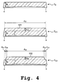
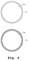
- Example 2 In the same manner as described in Example 1, a sputtering target having the target material Tc 1 in the shape illustrated in the cross-sectional view of Figure 4 and in the top view of Figure 6 was produced. Herein, a support member for the target material Tc 1 , which had the similar shape to that of Example 1, was employed.
- the target material Tc 1 is a target material which corresponds to the target material T 0 of Reference Example in the standard configuration wherein the thickness thereof is entirely uniform and increased by d 10 (see the cross-sectional view of Figure 4 ).
- the dotted line L represents the positon of the sputtering surface of the target material T 0 of the Reference Example in the standard configuration.
- the dimensions of the target material Tc 1 are as follows, respectively.
- Example 2 In the same manner as described in Example 1, a sputtering target having the target material Tc 2 in the shape illustrated in the cross-sectional view of Figure 4 and in the top view of Figure 6 was produced. Herein, a support member for the target material Tc 2 , which had the similar shape to that of Example 1, was employed.
- the target material Tc 2 is a target material which corresponds to the target material Tc 1 of Comparative Example 1 wherein the peripheral part has a step (see the cross-sectional view of Figure 4 ).
- Example 2 In the same manner as described in Example 1, a sputtering target having the target material Tc 3 in the shape illustrated in the cross-sectional view of Figure 5 and in the top view of Figure 7 was produced. Herein, a support member for the target material Tc 3 , which had the similar shape to that of Example 1, was employed.
- the target material Tc 3 is a target material which corresponds to the target material T 0 of the Reference Example in the standard configuration wherein the sputtering surface has a planar area 201 in a ring shape, which is protruded and formed concentrically (see the cross-sectional view of Figure 5 ).
- the dimensions of the target material Tc 3 are as follows, respectively.
- Example 2 In the same manner as described in Example 1, a sputtering target having the target material Tc 4 in the shape illustrated in the cross-sectional view of Figure 5 and in the top view of Figure 7 was produced.
- a support member for the target material Tc 4 which had the similar shape to that of Example 1, was employed.
- the target material Tc 4 is a target material which corresponds to the target material T 0 of the Reference Example in the standard configuration wherein the sputtering surface has double-ring shaped planar areas 202 (outer) and 203 (inner), which are protruded and formed concentrically (see the cross-sectional view of Figure 5 ).
- the dimensions of the target material Tc 4 are as follows, respectively.
- Example 2 In the same manner as described in Example 1, a sputtering target having the target material Tc 5 in the shape illustrated in the top and cross-sectional views of Figure 8 was produced. Herein, a support member for the target material Tc 5 , which had the same shape to that of Example 1, was employed.
- the target material Tc 5 has a configuration which mainly corresponds to that of the target material T of Example 1 ( Figure 2 ) wherein sizes of d 1 and d 2 are altered, and a step 9 is formed on the peripheral part 5 (see the cross-sectional view of Figure 8 ).
- the dimensions of the target material Tc 5 are as follows, respectively.
- Example 2 In the same manner as described in Example 1 except for the sizes of r 1 and d 5 were altered, a sputtering target having the target material Tc 6 was produced. Herein, a support member for the target material Tc 6 , which had the similar shape to that of Example 1, was employed.
- the dimensions of the target material Tc 6 are as follows, respectively.
- a magnetron sputtering apparatus (Endura 5500 (magnet: Dura-type) manufactured by Applied Materials, Inc.) and each of the sputtering targets of Example, Reference Example and Comparative Example were employed.
- a substrate having a diameter of 200 mm a silicon substrate manufactured by LG Siltron
- a thin coating layer was formed under the following conditions.
- the coating thicknesses were calculated from the sheet resistances ( ⁇ / ⁇ ) measured at the above-described 49 points. Therewith, standard deviations ⁇ (sigma) were calculated, and then, values of 1 ⁇ % (percent 1-sigma) were calculated.
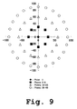
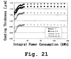
- a ratio of the coating thickness at 1 point at the central part (Point 1); 8 points around the center (Points 2-9 (in a distance from the center: 30 mm)); 16 points around them (Points 10-25 (in a distance from the center: 60 mm)); and 24 points around them (Points 26-49 (in a distance from the center: 90 mm)), respectively, as illustrated in Figure 9 , relative to the average value of the coating thicknesses calculated from the sheet resistances (( ⁇ / ⁇ ) measured at these 49 points was calculated in a percent (as a ratio of the coating thickness relative to the average coating thickness (in %)).
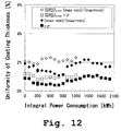
- the sputtering target of the Reference Example in the standard configuration had an excellent uniformity of the coating thickness. However, its life was 1200 kWh, which was not well sufficient.
- the sputtering target of Example 1 according to the present invention had a long life of 2000 kWh.
- the life of the sputtering target having the standard configuration according to the Reference Example was 1200 kWh (see Figures 10 and 12 ) as described above.
- the sputtering target of Example 1 according to the present invention had 1.5 times or more of life of that of the sputtering target having the standard configuration according to the Reference Example.
- the sputtering target of Example 1 according to the present invention had an excellent uniformity of the coating thickness all over the range from 0 to 2000 kWh) in comparison with the sputtering target having the standard configuration according to the Reference Example as described above.
- the sputtering target of Example 1 according to the present invention could provide an excellent uniformity of the coating thickness, all over the range from 0 to 2000 kWh, and all over the thin coating layer formed on the substrate.
- the sputtering target of Example 1 according to the present invention had a long life of 2000 kWh, and could provide an excellent uniformity of the coating thickness, all over the life of the range from 0 to 2000 kWh, and all over the substrate.
- the sputtering target according to Comparative Example 1 (using target material Tc 1 (see Figure 4 )) could be subjected to the sputtering till 2000 kWh.
- the uniformity of the coating thickness was remarkably deteriorated.
- the sputtering target according to Comparative Example 1 had a small coating thickness at the central part of the substrate (Point 1). Particularly, during the initial period (from 0 to 300 kWh), it was found that the thickness of the coating on the substrate at the central part (Point 1) was significantly small.
- the sputtering target according to Comparative Example 2 had a small thickness of the thin coating layer formed on the substrate at its circumference (Points 26-49) after/during the initial period immediately after the sputtering operation, and that an uniform coating thickness could not be obtained all over the substrate.
- the uniformity of the coating thickness was significantly deteriorated from/during the initial period of the sputtering.
- Figure 18 shows amount of erosion of the target material of the sputtering target according to Comparative Example 2.
- the solid line represents amount of erosion of the target material of the sputtering target according to Reference Example.
- the broken line represents amount of erosion of the target material of the sputtering target according to Comparative Example 2 (at every 400 kWh among 0-800 kWh).
- Example 1 it is also demonstrated that an excellent uniformity of the coating thickness can be obtained in the case that the target material has no step on its peripheral part.
- the uniformity of the coating thickness is surprisingly improved, in comparison with Reference Example and Comparative Example 1, in both of the initial period and the long term period, particularly in the initial period.
- Figure 19 shows erosion amount of the target material, which was measured on each of the sputtering targets of Reference Example, Comparative Example 1 and Example 1.
- the broken line represents erosion at Reference Example.
- the dotted line represents erosion at Comparative Example 1, and the solid line represents erosion at Example 1.
- the erosion amount was measured at 400, 800, 1200 and 2000 kWh, from 400 to 2000 kWh, respectively, with the proviso that the erosion amount was investigated till 1200 kWh for Reference Example.
- the erosion amount was increased over the area from 70 mm to 125 mm from the center on the sputtering target of Example 1 according to the present invention, particularly, from the area in a distance of about 90 mm from the center (i.e., about 56.4% of the radius (159.57 mm) of the sputtering surface) to the area in a distance of about 125 mm from the center (i.e., about 78.3% of the radius (159.57 mm) of the sputtering surface).
- the reasons why thickness of the thin coating layer thus formed on the substrate at the central part (Point 1) was extremely small are believed in that the increase in the thickness of the target material shortened the distance between the target material and the substrate (TS distance), and then, as shown in Figure 19 , the area around the circumference of the target material was deeply consumed, and therefore, the thickness of the coating layer formed on the area around the circumference of the substrate was increased, the amount of the coating layer formed on the central part (Point 1) of the substrate was relatively small.
- the thickness of the thin coating layer formed on the substrate at the central part was increased during the initial period of the sputtering, and the uniformity of the coating thickness could be improved.
- the value of d 1 was preferably set at 4.0 mm or less.
- the first area was positioned at a location lower than that of the second area by 15% of thickness of the second area at most. Thereby, the uniformity of the thickness of the thin coating layer formed on the substrate could be improved.
- the sputtering target according to the present invention can be utilized in a commercially available sputtering apparatus, particularly in a magnetron sputtering apparatus.
- the sputtering target provides a long life of 1800 kWh or more, as an integral power consumption, and, during the period, a thin coating layer with an excellent uniformity of its coating thickness can be formed on a substrate. Therefore, the sputtering target according to the present invention has benefits.
Landscapes
- Chemical & Material Sciences (AREA)
- Engineering & Computer Science (AREA)
- Physics & Mathematics (AREA)
- Plasma & Fusion (AREA)
- Analytical Chemistry (AREA)
- Chemical Kinetics & Catalysis (AREA)
- Materials Engineering (AREA)
- Mechanical Engineering (AREA)
- Metallurgy (AREA)
- Organic Chemistry (AREA)
- Physical Vapour Deposition (AREA)
- Electrodes Of Semiconductors (AREA)
Applications Claiming Priority (2)
| Application Number | Priority Date | Filing Date | Title |
|---|---|---|---|
| JP2014008740 | 2014-01-21 | ||
| PCT/JP2015/051395 WO2015111576A1 (ja) | 2014-01-21 | 2015-01-20 | スパッタリングターゲット |
Publications (3)
| Publication Number | Publication Date |
|---|---|
| EP3098332A1 true EP3098332A1 (de) | 2016-11-30 |
| EP3098332A4 EP3098332A4 (de) | 2017-06-28 |
| EP3098332B1 EP3098332B1 (de) | 2019-10-16 |
Family
ID=53681379
Family Applications (1)
| Application Number | Title | Priority Date | Filing Date |
|---|---|---|---|
| EP15741025.9A Active EP3098332B1 (de) | 2014-01-21 | 2015-01-20 | Sputter-target |
Country Status (9)
| Country | Link |
|---|---|
| US (1) | US11532468B2 (de) |
| EP (1) | EP3098332B1 (de) |
| JP (3) | JP6203870B2 (de) |
| KR (2) | KR20160111387A (de) |
| CN (1) | CN105934533B (de) |
| IL (1) | IL246811B (de) |
| MY (1) | MY180359A (de) |
| TW (1) | TWI678424B (de) |
| WO (1) | WO2015111576A1 (de) |
Families Citing this family (9)
| Publication number | Priority date | Publication date | Assignee | Title |
|---|---|---|---|---|
| CN105154836A (zh) * | 2015-09-18 | 2015-12-16 | 有研亿金新材料有限公司 | 一种高性能铁磁性溅射靶材 |
| CN106683988B (zh) * | 2016-12-28 | 2019-05-24 | 惠科股份有限公司 | 一种靶材装置 |
| JP6291122B1 (ja) | 2017-03-29 | 2018-03-14 | 住友化学株式会社 | スパッタリングターゲット |
| CN110010455A (zh) * | 2018-01-04 | 2019-07-12 | 合肥江丰电子材料有限公司 | 长寿命lcd靶材组件及其形成方法 |
| CN110029316A (zh) * | 2018-01-11 | 2019-07-19 | 合肥江丰电子材料有限公司 | 长寿命lcd靶材组件及其形成方法 |
| CN108624856B (zh) * | 2018-07-05 | 2024-06-25 | 包头稀土研究院 | 靶材组件 |
| CN109055900B (zh) * | 2018-09-17 | 2020-10-02 | 中国科学院宁波材料技术与工程研究所 | 一种用于阴极电弧沉积的复合靶及沉积方法 |
| CN110592406A (zh) * | 2019-10-10 | 2019-12-20 | 新疆众和股份有限公司 | 一种溅射用高纯铝铜合金靶材坯料的制备方法 |
| JP7511419B2 (ja) * | 2020-09-09 | 2024-07-05 | 東京エレクトロン株式会社 | 成膜方法、成膜装置及びプログラム |
Family Cites Families (23)
| Publication number | Priority date | Publication date | Assignee | Title |
|---|---|---|---|---|
| JPS4213030B1 (de) | 1962-07-19 | 1967-07-25 | ||
| JPS61183467A (ja) * | 1985-02-08 | 1986-08-16 | Hitachi Ltd | スパッタリング方法及びその装置 |
| JPS637366A (ja) * | 1986-06-27 | 1988-01-13 | Matsushita Electric Ind Co Ltd | マグネトロンスパツタ装置 |
| JPH04213030A (ja) | 1990-11-22 | 1992-08-04 | Tepitsuku:Kk | 紫外線強度計 |
| JPH05287524A (ja) | 1992-04-09 | 1993-11-02 | Anelva Corp | マグネトロンスパッタリング用ターゲット |
| JP2917743B2 (ja) * | 1993-04-23 | 1999-07-12 | 三菱マテリアル株式会社 | マグネトロンスパッタリング用Siターゲット材 |
| JPH08325719A (ja) | 1995-05-29 | 1996-12-10 | Sony Corp | スパッタ装置 |
| JPH09111445A (ja) * | 1995-10-12 | 1997-04-28 | Dainippon Printing Co Ltd | スパッタリングターゲット |
| US6086735A (en) | 1998-06-01 | 2000-07-11 | Praxair S.T. Technology, Inc. | Contoured sputtering target |
| JP4455689B2 (ja) | 1999-03-18 | 2010-04-21 | キヤノンアネルバ株式会社 | スパッタリング装置のマグネトロンカソード |
| JP2001140063A (ja) | 1999-09-23 | 2001-05-22 | Praxair St Technol Inc | 延長された寿命を有するスパッタターゲット |
| US6497797B1 (en) | 2000-08-21 | 2002-12-24 | Honeywell International Inc. | Methods of forming sputtering targets, and sputtering targets formed thereby |
| WO2002042518A1 (de) * | 2000-11-27 | 2002-05-30 | Unaxis Trading Ag | Target mit dickenprofilierung für rf manetron |
| US6872284B2 (en) | 2001-04-24 | 2005-03-29 | Tosoh Smd, Inc. | Target and method of optimizing target profile |
| US6638402B2 (en) | 2001-06-05 | 2003-10-28 | Praxair S.T. Technology, Inc. | Ring-type sputtering target |
| KR20040057287A (ko) | 2002-12-26 | 2004-07-02 | 삼성전자주식회사 | 스퍼터링용 타겟 |
| US6988306B2 (en) * | 2003-12-01 | 2006-01-24 | Praxair Technology, Inc. | High purity ferromagnetic sputter target, assembly and method of manufacturing same |
| JP2008038229A (ja) * | 2006-08-09 | 2008-02-21 | Mitsui Mining & Smelting Co Ltd | スパッタリング方法およびそれに用いられるスパッタリングターゲット |
| US20120097534A1 (en) * | 2008-08-29 | 2012-04-26 | Ulvac, Inc. | Magnetron sputtering cathode and film formation apparatus |
| US9752228B2 (en) | 2009-04-03 | 2017-09-05 | Applied Materials, Inc. | Sputtering target for PVD chamber |
| CN201793723U (zh) * | 2010-09-28 | 2011-04-13 | 宁波江丰电子材料有限公司 | 一种长寿命溅射靶材 |
| CN105008582A (zh) * | 2013-01-04 | 2015-10-28 | 东曹Smd有限公司 | 具有增强的表面轮廓和改善的性能的硅溅射靶及其制造方法 |
| US9779920B2 (en) * | 2013-08-14 | 2017-10-03 | Applied Materials, Inc. | Sputtering target with backside cooling grooves |
-
2015
- 2015-01-20 KR KR1020167019560A patent/KR20160111387A/ko not_active Ceased
- 2015-01-20 KR KR1020217013891A patent/KR20210055807A/ko not_active Ceased
- 2015-01-20 JP JP2015558852A patent/JP6203870B2/ja active Active
- 2015-01-20 EP EP15741025.9A patent/EP3098332B1/de active Active
- 2015-01-20 MY MYPI2016702597A patent/MY180359A/en unknown
- 2015-01-20 WO PCT/JP2015/051395 patent/WO2015111576A1/ja not_active Ceased
- 2015-01-20 TW TW104101813A patent/TWI678424B/zh active
- 2015-01-20 US US15/112,242 patent/US11532468B2/en active Active
- 2015-01-20 CN CN201580005170.1A patent/CN105934533B/zh active Active
-
2016
- 2016-07-18 IL IL246811A patent/IL246811B/en active IP Right Grant
-
2017
- 2017-06-06 JP JP2017111872A patent/JP6271796B2/ja active Active
- 2017-12-27 JP JP2017251213A patent/JP6514763B2/ja active Active
Also Published As
| Publication number | Publication date |
|---|---|
| JP2017179609A (ja) | 2017-10-05 |
| JPWO2015111576A1 (ja) | 2017-03-23 |
| US20160343551A1 (en) | 2016-11-24 |
| JP2018076598A (ja) | 2018-05-17 |
| JP6203870B2 (ja) | 2017-09-27 |
| JP6271796B2 (ja) | 2018-01-31 |
| KR20210055807A (ko) | 2021-05-17 |
| MY180359A (en) | 2020-11-28 |
| IL246811B (en) | 2019-12-31 |
| KR20160111387A (ko) | 2016-09-26 |
| TW201540857A (zh) | 2015-11-01 |
| JP6514763B2 (ja) | 2019-05-15 |
| EP3098332A4 (de) | 2017-06-28 |
| TWI678424B (zh) | 2019-12-01 |
| WO2015111576A1 (ja) | 2015-07-30 |
| EP3098332B1 (de) | 2019-10-16 |
| IL246811A0 (en) | 2016-08-31 |
| CN105934533B (zh) | 2018-11-27 |
| CN105934533A (zh) | 2016-09-07 |
| US11532468B2 (en) | 2022-12-20 |
Similar Documents
| Publication | Publication Date | Title |
|---|---|---|
| EP3098332B1 (de) | Sputter-target | |
| US6887356B2 (en) | Hollow cathode target and methods of making same | |
| TWI605142B (zh) | 具有增進的表面輪廓和改善的性能的矽濺射靶及製造其之方法 | |
| CN102513353B (zh) | 溅射靶及制造方法 | |
| CN104018128B (zh) | 一种镍铂合金溅射靶材及其制备方法 | |
| JP2011517329A (ja) | 寿命を延ばしスパッタリング均一性を高めたスパッタリングターゲット | |
| KR20010049969A (ko) | 클래드 중공 음극 마그네트론 스퍼터 타겟의 제조방법 | |
| KR102338193B1 (ko) | 스퍼터링 타깃 | |
| WO2010085316A1 (en) | Monolithic aluminum alloy target and method of manufacturing | |
| KR102080367B1 (ko) | 스퍼터링용 티탄 타깃 | |
| JP2001140063A (ja) | 延長された寿命を有するスパッタターゲット | |
| US12020916B2 (en) | Niobium sputtering target | |
| TWI853684B (zh) | 濺鍍靶及其製造方法 | |
| JP2015025170A (ja) | シリコンターゲット | |
| JPWO2018235889A1 (ja) | スパッタリングターゲット材、スパッタリングターゲット、スパッタリングターゲット用アルミニウム板及びその製造方法 |
Legal Events
| Date | Code | Title | Description |
|---|---|---|---|
| PUAI | Public reference made under article 153(3) epc to a published international application that has entered the european phase |
Free format text: ORIGINAL CODE: 0009012 |
|
| 17P | Request for examination filed |
Effective date: 20160720 |
|
| AK | Designated contracting states |
Kind code of ref document: A1 Designated state(s): AL AT BE BG CH CY CZ DE DK EE ES FI FR GB GR HR HU IE IS IT LI LT LU LV MC MK MT NL NO PL PT RO RS SE SI SK SM TR |
|
| AX | Request for extension of the european patent |
Extension state: BA ME |
|
| DAX | Request for extension of the european patent (deleted) | ||
| A4 | Supplementary search report drawn up and despatched |
Effective date: 20170529 |
|
| RIC1 | Information provided on ipc code assigned before grant |
Ipc: C23C 14/34 20060101AFI20170522BHEP Ipc: H01J 37/34 20060101ALI20170522BHEP Ipc: H01L 21/285 20060101ALI20170522BHEP |
|
| GRAP | Despatch of communication of intention to grant a patent |
Free format text: ORIGINAL CODE: EPIDOSNIGR1 |
|
| STAA | Information on the status of an ep patent application or granted ep patent |
Free format text: STATUS: GRANT OF PATENT IS INTENDED |
|
| INTG | Intention to grant announced |
Effective date: 20190621 |
|
| GRAS | Grant fee paid |
Free format text: ORIGINAL CODE: EPIDOSNIGR3 |
|
| GRAA | (expected) grant |
Free format text: ORIGINAL CODE: 0009210 |
|
| STAA | Information on the status of an ep patent application or granted ep patent |
Free format text: STATUS: THE PATENT HAS BEEN GRANTED |
|
| AK | Designated contracting states |
Kind code of ref document: B1 Designated state(s): AL AT BE BG CH CY CZ DE DK EE ES FI FR GB GR HR HU IE IS IT LI LT LU LV MC MK MT NL NO PL PT RO RS SE SI SK SM TR |
|
| REG | Reference to a national code |
Ref country code: GB Ref legal event code: FG4D |
|
| REG | Reference to a national code |
Ref country code: CH Ref legal event code: EP |
|
| REG | Reference to a national code |
Ref country code: DE Ref legal event code: R096 Ref document number: 602015039911 Country of ref document: DE |
|
| REG | Reference to a national code |
Ref country code: IE Ref legal event code: FG4D |
|
| REG | Reference to a national code |
Ref country code: AT Ref legal event code: REF Ref document number: 1191325 Country of ref document: AT Kind code of ref document: T Effective date: 20191115 |
|
| REG | Reference to a national code |
Ref country code: NL Ref legal event code: MP Effective date: 20191016 |
|
| REG | Reference to a national code |
Ref country code: LT Ref legal event code: MG4D |
|
| REG | Reference to a national code |
Ref country code: AT Ref legal event code: MK05 Ref document number: 1191325 Country of ref document: AT Kind code of ref document: T Effective date: 20191016 |
|
| PG25 | Lapsed in a contracting state [announced via postgrant information from national office to epo] |
Ref country code: LT Free format text: LAPSE BECAUSE OF FAILURE TO SUBMIT A TRANSLATION OF THE DESCRIPTION OR TO PAY THE FEE WITHIN THE PRESCRIBED TIME-LIMIT Effective date: 20191016 Ref country code: PL Free format text: LAPSE BECAUSE OF FAILURE TO SUBMIT A TRANSLATION OF THE DESCRIPTION OR TO PAY THE FEE WITHIN THE PRESCRIBED TIME-LIMIT Effective date: 20191016 Ref country code: NL Free format text: LAPSE BECAUSE OF FAILURE TO SUBMIT A TRANSLATION OF THE DESCRIPTION OR TO PAY THE FEE WITHIN THE PRESCRIBED TIME-LIMIT Effective date: 20191016 Ref country code: LV Free format text: LAPSE BECAUSE OF FAILURE TO SUBMIT A TRANSLATION OF THE DESCRIPTION OR TO PAY THE FEE WITHIN THE PRESCRIBED TIME-LIMIT Effective date: 20191016 Ref country code: PT Free format text: LAPSE BECAUSE OF FAILURE TO SUBMIT A TRANSLATION OF THE DESCRIPTION OR TO PAY THE FEE WITHIN THE PRESCRIBED TIME-LIMIT Effective date: 20200217 Ref country code: FI Free format text: LAPSE BECAUSE OF FAILURE TO SUBMIT A TRANSLATION OF THE DESCRIPTION OR TO PAY THE FEE WITHIN THE PRESCRIBED TIME-LIMIT Effective date: 20191016 Ref country code: SE Free format text: LAPSE BECAUSE OF FAILURE TO SUBMIT A TRANSLATION OF THE DESCRIPTION OR TO PAY THE FEE WITHIN THE PRESCRIBED TIME-LIMIT Effective date: 20191016 Ref country code: AT Free format text: LAPSE BECAUSE OF FAILURE TO SUBMIT A TRANSLATION OF THE DESCRIPTION OR TO PAY THE FEE WITHIN THE PRESCRIBED TIME-LIMIT Effective date: 20191016 Ref country code: BG Free format text: LAPSE BECAUSE OF FAILURE TO SUBMIT A TRANSLATION OF THE DESCRIPTION OR TO PAY THE FEE WITHIN THE PRESCRIBED TIME-LIMIT Effective date: 20200116 Ref country code: GR Free format text: LAPSE BECAUSE OF FAILURE TO SUBMIT A TRANSLATION OF THE DESCRIPTION OR TO PAY THE FEE WITHIN THE PRESCRIBED TIME-LIMIT Effective date: 20200117 Ref country code: NO Free format text: LAPSE BECAUSE OF FAILURE TO SUBMIT A TRANSLATION OF THE DESCRIPTION OR TO PAY THE FEE WITHIN THE PRESCRIBED TIME-LIMIT Effective date: 20200116 |
|
| PG25 | Lapsed in a contracting state [announced via postgrant information from national office to epo] |
Ref country code: IS Free format text: LAPSE BECAUSE OF FAILURE TO SUBMIT A TRANSLATION OF THE DESCRIPTION OR TO PAY THE FEE WITHIN THE PRESCRIBED TIME-LIMIT Effective date: 20200224 Ref country code: RS Free format text: LAPSE BECAUSE OF FAILURE TO SUBMIT A TRANSLATION OF THE DESCRIPTION OR TO PAY THE FEE WITHIN THE PRESCRIBED TIME-LIMIT Effective date: 20191016 Ref country code: HR Free format text: LAPSE BECAUSE OF FAILURE TO SUBMIT A TRANSLATION OF THE DESCRIPTION OR TO PAY THE FEE WITHIN THE PRESCRIBED TIME-LIMIT Effective date: 20191016 |
|
| PG25 | Lapsed in a contracting state [announced via postgrant information from national office to epo] |
Ref country code: AL Free format text: LAPSE BECAUSE OF FAILURE TO SUBMIT A TRANSLATION OF THE DESCRIPTION OR TO PAY THE FEE WITHIN THE PRESCRIBED TIME-LIMIT Effective date: 20191016 |
|
| REG | Reference to a national code |
Ref country code: DE Ref legal event code: R097 Ref document number: 602015039911 Country of ref document: DE |
|
| PG2D | Information on lapse in contracting state deleted |
Ref country code: IS |
|
| PG25 | Lapsed in a contracting state [announced via postgrant information from national office to epo] |
Ref country code: IS Free format text: LAPSE BECAUSE OF FAILURE TO SUBMIT A TRANSLATION OF THE DESCRIPTION OR TO PAY THE FEE WITHIN THE PRESCRIBED TIME-LIMIT Effective date: 20200216 Ref country code: DK Free format text: LAPSE BECAUSE OF FAILURE TO SUBMIT A TRANSLATION OF THE DESCRIPTION OR TO PAY THE FEE WITHIN THE PRESCRIBED TIME-LIMIT Effective date: 20191016 Ref country code: EE Free format text: LAPSE BECAUSE OF FAILURE TO SUBMIT A TRANSLATION OF THE DESCRIPTION OR TO PAY THE FEE WITHIN THE PRESCRIBED TIME-LIMIT Effective date: 20191016 Ref country code: RO Free format text: LAPSE BECAUSE OF FAILURE TO SUBMIT A TRANSLATION OF THE DESCRIPTION OR TO PAY THE FEE WITHIN THE PRESCRIBED TIME-LIMIT Effective date: 20191016 Ref country code: ES Free format text: LAPSE BECAUSE OF FAILURE TO SUBMIT A TRANSLATION OF THE DESCRIPTION OR TO PAY THE FEE WITHIN THE PRESCRIBED TIME-LIMIT Effective date: 20191016 |
|
| PLBE | No opposition filed within time limit |
Free format text: ORIGINAL CODE: 0009261 |
|
| STAA | Information on the status of an ep patent application or granted ep patent |
Free format text: STATUS: NO OPPOSITION FILED WITHIN TIME LIMIT |
|
| PG25 | Lapsed in a contracting state [announced via postgrant information from national office to epo] |
Ref country code: SK Free format text: LAPSE BECAUSE OF FAILURE TO SUBMIT A TRANSLATION OF THE DESCRIPTION OR TO PAY THE FEE WITHIN THE PRESCRIBED TIME-LIMIT Effective date: 20191016 Ref country code: SM Free format text: LAPSE BECAUSE OF FAILURE TO SUBMIT A TRANSLATION OF THE DESCRIPTION OR TO PAY THE FEE WITHIN THE PRESCRIBED TIME-LIMIT Effective date: 20191016 Ref country code: MC Free format text: LAPSE BECAUSE OF FAILURE TO SUBMIT A TRANSLATION OF THE DESCRIPTION OR TO PAY THE FEE WITHIN THE PRESCRIBED TIME-LIMIT Effective date: 20191016 |
|
| REG | Reference to a national code |
Ref country code: CH Ref legal event code: PL |
|
| 26N | No opposition filed |
Effective date: 20200717 |
|
| GBPC | Gb: european patent ceased through non-payment of renewal fee |
Effective date: 20200120 |
|
| REG | Reference to a national code |
Ref country code: BE Ref legal event code: MM Effective date: 20200131 |
|
| PG25 | Lapsed in a contracting state [announced via postgrant information from national office to epo] |
Ref country code: LU Free format text: LAPSE BECAUSE OF NON-PAYMENT OF DUE FEES Effective date: 20200120 Ref country code: GB Free format text: LAPSE BECAUSE OF NON-PAYMENT OF DUE FEES Effective date: 20200120 |
|
| PG25 | Lapsed in a contracting state [announced via postgrant information from national office to epo] |
Ref country code: BE Free format text: LAPSE BECAUSE OF NON-PAYMENT OF DUE FEES Effective date: 20200131 Ref country code: SI Free format text: LAPSE BECAUSE OF FAILURE TO SUBMIT A TRANSLATION OF THE DESCRIPTION OR TO PAY THE FEE WITHIN THE PRESCRIBED TIME-LIMIT Effective date: 20191016 Ref country code: LI Free format text: LAPSE BECAUSE OF NON-PAYMENT OF DUE FEES Effective date: 20200131 Ref country code: CH Free format text: LAPSE BECAUSE OF NON-PAYMENT OF DUE FEES Effective date: 20200131 |
|
| PG25 | Lapsed in a contracting state [announced via postgrant information from national office to epo] |
Ref country code: IE Free format text: LAPSE BECAUSE OF NON-PAYMENT OF DUE FEES Effective date: 20200120 |
|
| PG25 | Lapsed in a contracting state [announced via postgrant information from national office to epo] |
Ref country code: TR Free format text: LAPSE BECAUSE OF FAILURE TO SUBMIT A TRANSLATION OF THE DESCRIPTION OR TO PAY THE FEE WITHIN THE PRESCRIBED TIME-LIMIT Effective date: 20191016 Ref country code: MT Free format text: LAPSE BECAUSE OF FAILURE TO SUBMIT A TRANSLATION OF THE DESCRIPTION OR TO PAY THE FEE WITHIN THE PRESCRIBED TIME-LIMIT Effective date: 20191016 Ref country code: CY Free format text: LAPSE BECAUSE OF FAILURE TO SUBMIT A TRANSLATION OF THE DESCRIPTION OR TO PAY THE FEE WITHIN THE PRESCRIBED TIME-LIMIT Effective date: 20191016 |
|
| PG25 | Lapsed in a contracting state [announced via postgrant information from national office to epo] |
Ref country code: MK Free format text: LAPSE BECAUSE OF FAILURE TO SUBMIT A TRANSLATION OF THE DESCRIPTION OR TO PAY THE FEE WITHIN THE PRESCRIBED TIME-LIMIT Effective date: 20191016 |
|
| PGFP | Annual fee paid to national office [announced via postgrant information from national office to epo] |
Ref country code: FR Payment date: 20251217 Year of fee payment: 12 |
|
| PGFP | Annual fee paid to national office [announced via postgrant information from national office to epo] |
Ref country code: DE Payment date: 20251217 Year of fee payment: 12 |
|
| PGFP | Annual fee paid to national office [announced via postgrant information from national office to epo] |
Ref country code: IT Payment date: 20260107 Year of fee payment: 12 |
|
| PGFP | Annual fee paid to national office [announced via postgrant information from national office to epo] |
Ref country code: CZ Payment date: 20260105 Year of fee payment: 12 |