JP6203870B2 - スパッタリングターゲット - Google Patents
スパッタリングターゲット Download PDFInfo
- Publication number
- JP6203870B2 JP6203870B2 JP2015558852A JP2015558852A JP6203870B2 JP 6203870 B2 JP6203870 B2 JP 6203870B2 JP 2015558852 A JP2015558852 A JP 2015558852A JP 2015558852 A JP2015558852 A JP 2015558852A JP 6203870 B2 JP6203870 B2 JP 6203870B2
- Authority
- JP
- Japan
- Prior art keywords
- region
- sputtering
- target material
- target
- sputtering target
- Prior art date
- Legal status (The legal status is an assumption and is not a legal conclusion. Google has not performed a legal analysis and makes no representation as to the accuracy of the status listed.)
- Active
Links
Images


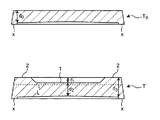


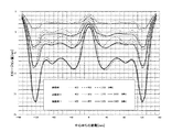


Classifications
-
- H—ELECTRICITY
- H01—ELECTRIC ELEMENTS
- H01J—ELECTRIC DISCHARGE TUBES OR DISCHARGE LAMPS
- H01J37/00—Discharge tubes with provision for introducing objects or material to be exposed to the discharge, e.g. for the purpose of examination or processing thereof
- H01J37/32—Gas-filled discharge tubes
- H01J37/34—Gas-filled discharge tubes operating with cathodic sputtering
- H01J37/3411—Constructional aspects of the reactor
- H01J37/3414—Targets
- H01J37/3423—Shape
-
- C—CHEMISTRY; METALLURGY
- C23—COATING METALLIC MATERIAL; COATING MATERIAL WITH METALLIC MATERIAL; CHEMICAL SURFACE TREATMENT; DIFFUSION TREATMENT OF METALLIC MATERIAL; COATING BY VACUUM EVAPORATION, BY SPUTTERING, BY ION IMPLANTATION OR BY CHEMICAL VAPOUR DEPOSITION, IN GENERAL; INHIBITING CORROSION OF METALLIC MATERIAL OR INCRUSTATION IN GENERAL
- C23C—COATING METALLIC MATERIAL; COATING MATERIAL WITH METALLIC MATERIAL; SURFACE TREATMENT OF METALLIC MATERIAL BY DIFFUSION INTO THE SURFACE, BY CHEMICAL CONVERSION OR SUBSTITUTION; COATING BY VACUUM EVAPORATION, BY SPUTTERING, BY ION IMPLANTATION OR BY CHEMICAL VAPOUR DEPOSITION, IN GENERAL
- C23C14/00—Coating by vacuum evaporation, by sputtering or by ion implantation of the coating forming material
- C23C14/22—Coating by vacuum evaporation, by sputtering or by ion implantation of the coating forming material characterised by the process of coating
- C23C14/34—Sputtering
- C23C14/3407—Cathode assembly for sputtering apparatus, e.g. Target
-
- H—ELECTRICITY
- H01—ELECTRIC ELEMENTS
- H01J—ELECTRIC DISCHARGE TUBES OR DISCHARGE LAMPS
- H01J37/00—Discharge tubes with provision for introducing objects or material to be exposed to the discharge, e.g. for the purpose of examination or processing thereof
- H01J37/32—Gas-filled discharge tubes
- H01J37/34—Gas-filled discharge tubes operating with cathodic sputtering
- H01J37/3411—Constructional aspects of the reactor
- H01J37/3414—Targets
-
- H—ELECTRICITY
- H01—ELECTRIC ELEMENTS
- H01J—ELECTRIC DISCHARGE TUBES OR DISCHARGE LAMPS
- H01J37/00—Discharge tubes with provision for introducing objects or material to be exposed to the discharge, e.g. for the purpose of examination or processing thereof
- H01J37/32—Gas-filled discharge tubes
- H01J37/34—Gas-filled discharge tubes operating with cathodic sputtering
- H01J37/3411—Constructional aspects of the reactor
- H01J37/3414—Targets
- H01J37/3426—Material
-
- H—ELECTRICITY
- H01—ELECTRIC ELEMENTS
- H01J—ELECTRIC DISCHARGE TUBES OR DISCHARGE LAMPS
- H01J2237/00—Discharge tubes exposing object to beam, e.g. for analysis treatment, etching, imaging
- H01J2237/32—Processing objects by plasma generation
- H01J2237/33—Processing objects by plasma generation characterised by the type of processing
- H01J2237/332—Coating
Landscapes
- Chemical & Material Sciences (AREA)
- Engineering & Computer Science (AREA)
- Physics & Mathematics (AREA)
- Plasma & Fusion (AREA)
- Analytical Chemistry (AREA)
- Chemical Kinetics & Catalysis (AREA)
- Materials Engineering (AREA)
- Mechanical Engineering (AREA)
- Metallurgy (AREA)
- Organic Chemistry (AREA)
- Physical Vapour Deposition (AREA)
- Electrodes Of Semiconductors (AREA)
Applications Claiming Priority (3)
| Application Number | Priority Date | Filing Date | Title |
|---|---|---|---|
| JP2014008740 | 2014-01-21 | ||
| JP2014008740 | 2014-01-21 | ||
| PCT/JP2015/051395 WO2015111576A1 (ja) | 2014-01-21 | 2015-01-20 | スパッタリングターゲット |
Related Child Applications (1)
| Application Number | Title | Priority Date | Filing Date |
|---|---|---|---|
| JP2017111872A Division JP6271796B2 (ja) | 2014-01-21 | 2017-06-06 | スパッタリングターゲット |
Publications (2)
| Publication Number | Publication Date |
|---|---|
| JPWO2015111576A1 JPWO2015111576A1 (ja) | 2017-03-23 |
| JP6203870B2 true JP6203870B2 (ja) | 2017-09-27 |
Family
ID=53681379
Family Applications (3)
| Application Number | Title | Priority Date | Filing Date |
|---|---|---|---|
| JP2015558852A Active JP6203870B2 (ja) | 2014-01-21 | 2015-01-20 | スパッタリングターゲット |
| JP2017111872A Active JP6271796B2 (ja) | 2014-01-21 | 2017-06-06 | スパッタリングターゲット |
| JP2017251213A Active JP6514763B2 (ja) | 2014-01-21 | 2017-12-27 | スパッタリングターゲット |
Family Applications After (2)
| Application Number | Title | Priority Date | Filing Date |
|---|---|---|---|
| JP2017111872A Active JP6271796B2 (ja) | 2014-01-21 | 2017-06-06 | スパッタリングターゲット |
| JP2017251213A Active JP6514763B2 (ja) | 2014-01-21 | 2017-12-27 | スパッタリングターゲット |
Country Status (9)
| Country | Link |
|---|---|
| US (1) | US11532468B2 (de) |
| EP (1) | EP3098332B1 (de) |
| JP (3) | JP6203870B2 (de) |
| KR (2) | KR20160111387A (de) |
| CN (1) | CN105934533B (de) |
| IL (1) | IL246811B (de) |
| MY (1) | MY180359A (de) |
| TW (1) | TWI678424B (de) |
| WO (1) | WO2015111576A1 (de) |
Families Citing this family (9)
| Publication number | Priority date | Publication date | Assignee | Title |
|---|---|---|---|---|
| CN105154836A (zh) * | 2015-09-18 | 2015-12-16 | 有研亿金新材料有限公司 | 一种高性能铁磁性溅射靶材 |
| CN106683988B (zh) * | 2016-12-28 | 2019-05-24 | 惠科股份有限公司 | 一种靶材装置 |
| JP6291122B1 (ja) | 2017-03-29 | 2018-03-14 | 住友化学株式会社 | スパッタリングターゲット |
| CN110010455A (zh) * | 2018-01-04 | 2019-07-12 | 合肥江丰电子材料有限公司 | 长寿命lcd靶材组件及其形成方法 |
| CN110029316A (zh) * | 2018-01-11 | 2019-07-19 | 合肥江丰电子材料有限公司 | 长寿命lcd靶材组件及其形成方法 |
| CN108624856B (zh) * | 2018-07-05 | 2024-06-25 | 包头稀土研究院 | 靶材组件 |
| CN109055900B (zh) * | 2018-09-17 | 2020-10-02 | 中国科学院宁波材料技术与工程研究所 | 一种用于阴极电弧沉积的复合靶及沉积方法 |
| CN110592406A (zh) * | 2019-10-10 | 2019-12-20 | 新疆众和股份有限公司 | 一种溅射用高纯铝铜合金靶材坯料的制备方法 |
| JP7511419B2 (ja) * | 2020-09-09 | 2024-07-05 | 東京エレクトロン株式会社 | 成膜方法、成膜装置及びプログラム |
Family Cites Families (23)
| Publication number | Priority date | Publication date | Assignee | Title |
|---|---|---|---|---|
| JPS4213030B1 (de) | 1962-07-19 | 1967-07-25 | ||
| JPS61183467A (ja) * | 1985-02-08 | 1986-08-16 | Hitachi Ltd | スパッタリング方法及びその装置 |
| JPS637366A (ja) * | 1986-06-27 | 1988-01-13 | Matsushita Electric Ind Co Ltd | マグネトロンスパツタ装置 |
| JPH04213030A (ja) | 1990-11-22 | 1992-08-04 | Tepitsuku:Kk | 紫外線強度計 |
| JPH05287524A (ja) | 1992-04-09 | 1993-11-02 | Anelva Corp | マグネトロンスパッタリング用ターゲット |
| JP2917743B2 (ja) * | 1993-04-23 | 1999-07-12 | 三菱マテリアル株式会社 | マグネトロンスパッタリング用Siターゲット材 |
| JPH08325719A (ja) | 1995-05-29 | 1996-12-10 | Sony Corp | スパッタ装置 |
| JPH09111445A (ja) * | 1995-10-12 | 1997-04-28 | Dainippon Printing Co Ltd | スパッタリングターゲット |
| US6086735A (en) | 1998-06-01 | 2000-07-11 | Praxair S.T. Technology, Inc. | Contoured sputtering target |
| JP4455689B2 (ja) | 1999-03-18 | 2010-04-21 | キヤノンアネルバ株式会社 | スパッタリング装置のマグネトロンカソード |
| JP2001140063A (ja) | 1999-09-23 | 2001-05-22 | Praxair St Technol Inc | 延長された寿命を有するスパッタターゲット |
| US6497797B1 (en) | 2000-08-21 | 2002-12-24 | Honeywell International Inc. | Methods of forming sputtering targets, and sputtering targets formed thereby |
| WO2002042518A1 (de) * | 2000-11-27 | 2002-05-30 | Unaxis Trading Ag | Target mit dickenprofilierung für rf manetron |
| US6872284B2 (en) | 2001-04-24 | 2005-03-29 | Tosoh Smd, Inc. | Target and method of optimizing target profile |
| US6638402B2 (en) | 2001-06-05 | 2003-10-28 | Praxair S.T. Technology, Inc. | Ring-type sputtering target |
| KR20040057287A (ko) | 2002-12-26 | 2004-07-02 | 삼성전자주식회사 | 스퍼터링용 타겟 |
| US6988306B2 (en) * | 2003-12-01 | 2006-01-24 | Praxair Technology, Inc. | High purity ferromagnetic sputter target, assembly and method of manufacturing same |
| JP2008038229A (ja) * | 2006-08-09 | 2008-02-21 | Mitsui Mining & Smelting Co Ltd | スパッタリング方法およびそれに用いられるスパッタリングターゲット |
| US20120097534A1 (en) * | 2008-08-29 | 2012-04-26 | Ulvac, Inc. | Magnetron sputtering cathode and film formation apparatus |
| US9752228B2 (en) | 2009-04-03 | 2017-09-05 | Applied Materials, Inc. | Sputtering target for PVD chamber |
| CN201793723U (zh) * | 2010-09-28 | 2011-04-13 | 宁波江丰电子材料有限公司 | 一种长寿命溅射靶材 |
| CN105008582A (zh) * | 2013-01-04 | 2015-10-28 | 东曹Smd有限公司 | 具有增强的表面轮廓和改善的性能的硅溅射靶及其制造方法 |
| US9779920B2 (en) * | 2013-08-14 | 2017-10-03 | Applied Materials, Inc. | Sputtering target with backside cooling grooves |
-
2015
- 2015-01-20 KR KR1020167019560A patent/KR20160111387A/ko not_active Ceased
- 2015-01-20 KR KR1020217013891A patent/KR20210055807A/ko not_active Ceased
- 2015-01-20 JP JP2015558852A patent/JP6203870B2/ja active Active
- 2015-01-20 EP EP15741025.9A patent/EP3098332B1/de active Active
- 2015-01-20 MY MYPI2016702597A patent/MY180359A/en unknown
- 2015-01-20 WO PCT/JP2015/051395 patent/WO2015111576A1/ja not_active Ceased
- 2015-01-20 TW TW104101813A patent/TWI678424B/zh active
- 2015-01-20 US US15/112,242 patent/US11532468B2/en active Active
- 2015-01-20 CN CN201580005170.1A patent/CN105934533B/zh active Active
-
2016
- 2016-07-18 IL IL246811A patent/IL246811B/en active IP Right Grant
-
2017
- 2017-06-06 JP JP2017111872A patent/JP6271796B2/ja active Active
- 2017-12-27 JP JP2017251213A patent/JP6514763B2/ja active Active
Also Published As
| Publication number | Publication date |
|---|---|
| JP2017179609A (ja) | 2017-10-05 |
| JPWO2015111576A1 (ja) | 2017-03-23 |
| US20160343551A1 (en) | 2016-11-24 |
| JP2018076598A (ja) | 2018-05-17 |
| JP6271796B2 (ja) | 2018-01-31 |
| KR20210055807A (ko) | 2021-05-17 |
| MY180359A (en) | 2020-11-28 |
| IL246811B (en) | 2019-12-31 |
| KR20160111387A (ko) | 2016-09-26 |
| TW201540857A (zh) | 2015-11-01 |
| JP6514763B2 (ja) | 2019-05-15 |
| EP3098332A4 (de) | 2017-06-28 |
| TWI678424B (zh) | 2019-12-01 |
| WO2015111576A1 (ja) | 2015-07-30 |
| EP3098332B1 (de) | 2019-10-16 |
| IL246811A0 (en) | 2016-08-31 |
| CN105934533B (zh) | 2018-11-27 |
| CN105934533A (zh) | 2016-09-07 |
| EP3098332A1 (de) | 2016-11-30 |
| US11532468B2 (en) | 2022-12-20 |
Similar Documents
| Publication | Publication Date | Title |
|---|---|---|
| JP6271796B2 (ja) | スパッタリングターゲット | |
| TWI605142B (zh) | 具有增進的表面輪廓和改善的性能的矽濺射靶及製造其之方法 | |
| US6887356B2 (en) | Hollow cathode target and methods of making same | |
| JP6077102B2 (ja) | スパッタリング用チタンターゲット及びその製造方法 | |
| JP2012522894A (ja) | Pvdチャンバ用スパッターターゲット | |
| US9147558B2 (en) | Finned shutter disk for a substrate process chamber | |
| KR102338193B1 (ko) | 스퍼터링 타깃 | |
| JP7427061B2 (ja) | プロファイルされたスパッタリングターゲット及びその製造方法 | |
| KR20060033013A (ko) | 저 전도 백킹 플레이트를 갖는 스퍼터링 타겟 조립체 및 그제조 방법 | |
| JP2015025170A (ja) | シリコンターゲット |
Legal Events
| Date | Code | Title | Description |
|---|---|---|---|
| A131 | Notification of reasons for refusal |
Free format text: JAPANESE INTERMEDIATE CODE: A131 Effective date: 20161122 |
|
| A521 | Request for written amendment filed |
Free format text: JAPANESE INTERMEDIATE CODE: A523 Effective date: 20170120 |
|
| A02 | Decision of refusal |
Free format text: JAPANESE INTERMEDIATE CODE: A02 Effective date: 20170307 |
|
| A521 | Request for written amendment filed |
Free format text: JAPANESE INTERMEDIATE CODE: A523 Effective date: 20170606 |
|
| A911 | Transfer to examiner for re-examination before appeal (zenchi) |
Free format text: JAPANESE INTERMEDIATE CODE: A911 Effective date: 20170614 |
|
| TRDD | Decision of grant or rejection written | ||
| A01 | Written decision to grant a patent or to grant a registration (utility model) |
Free format text: JAPANESE INTERMEDIATE CODE: A01 Effective date: 20170822 |
|
| A61 | First payment of annual fees (during grant procedure) |
Free format text: JAPANESE INTERMEDIATE CODE: A61 Effective date: 20170830 |
|
| R150 | Certificate of patent or registration of utility model |
Ref document number: 6203870 Country of ref document: JP Free format text: JAPANESE INTERMEDIATE CODE: R150 |
|
| S531 | Written request for registration of change of domicile |
Free format text: JAPANESE INTERMEDIATE CODE: R313531 |
|
| R350 | Written notification of registration of transfer |
Free format text: JAPANESE INTERMEDIATE CODE: R350 |