EP3100310B1 - Procédé de production d'une carte de circuits imprimés - Google Patents
Procédé de production d'une carte de circuits imprimés Download PDFInfo
- Publication number
- EP3100310B1 EP3100310B1 EP15708697.6A EP15708697A EP3100310B1 EP 3100310 B1 EP3100310 B1 EP 3100310B1 EP 15708697 A EP15708697 A EP 15708697A EP 3100310 B1 EP3100310 B1 EP 3100310B1
- Authority
- EP
- European Patent Office
- Prior art keywords
- circuit board
- layer
- printed circuit
- cavity
- protective layer
- Prior art date
- Legal status (The legal status is an assumption and is not a legal conclusion. Google has not performed a legal analysis and makes no representation as to the accuracy of the status listed.)
- Active
Links
Images

Classifications
-
- H—ELECTRICITY
- H05—ELECTRIC TECHNIQUES NOT OTHERWISE PROVIDED FOR
- H05K—PRINTED CIRCUITS; CASINGS OR CONSTRUCTIONAL DETAILS OF ELECTRIC APPARATUS; MANUFACTURE OF ASSEMBLAGES OF ELECTRICAL COMPONENTS
- H05K1/00—Printed circuits
- H05K1/02—Details
- H05K1/0274—Optical details, e.g. printed circuits comprising integral optical means
-
- H—ELECTRICITY
- H05—ELECTRIC TECHNIQUES NOT OTHERWISE PROVIDED FOR
- H05K—PRINTED CIRCUITS; CASINGS OR CONSTRUCTIONAL DETAILS OF ELECTRIC APPARATUS; MANUFACTURE OF ASSEMBLAGES OF ELECTRICAL COMPONENTS
- H05K1/00—Printed circuits
- H05K1/18—Printed circuits structurally associated with non-printed electric components
- H05K1/182—Printed circuits structurally associated with non-printed electric components associated with components mounted in printed circuit boards [PCB], e.g. insert-mounted components [IMC]
- H05K1/183—Printed circuits structurally associated with non-printed electric components associated with components mounted in printed circuit boards [PCB], e.g. insert-mounted components [IMC] associated with components mounted in and supported by recessed areas of the PCBs
-
- H—ELECTRICITY
- H05—ELECTRIC TECHNIQUES NOT OTHERWISE PROVIDED FOR
- H05K—PRINTED CIRCUITS; CASINGS OR CONSTRUCTIONAL DETAILS OF ELECTRIC APPARATUS; MANUFACTURE OF ASSEMBLAGES OF ELECTRICAL COMPONENTS
- H05K3/00—Apparatus or processes for manufacturing printed circuits
- H05K3/0011—Working of insulating substrates or insulating layers
- H05K3/0017—Etching of the substrate by chemical or physical means
- H05K3/0026—Etching of the substrate by chemical or physical means by laser ablation
-
- H—ELECTRICITY
- H05—ELECTRIC TECHNIQUES NOT OTHERWISE PROVIDED FOR
- H05K—PRINTED CIRCUITS; CASINGS OR CONSTRUCTIONAL DETAILS OF ELECTRIC APPARATUS; MANUFACTURE OF ASSEMBLAGES OF ELECTRICAL COMPONENTS
- H05K3/00—Apparatus or processes for manufacturing printed circuits
- H05K3/0011—Working of insulating substrates or insulating layers
- H05K3/0044—Mechanical working of the substrate, e.g. drilling or punching
-
- H—ELECTRICITY
- H05—ELECTRIC TECHNIQUES NOT OTHERWISE PROVIDED FOR
- H05K—PRINTED CIRCUITS; CASINGS OR CONSTRUCTIONAL DETAILS OF ELECTRIC APPARATUS; MANUFACTURE OF ASSEMBLAGES OF ELECTRICAL COMPONENTS
- H05K3/00—Apparatus or processes for manufacturing printed circuits
- H05K3/0011—Working of insulating substrates or insulating layers
- H05K3/0055—After-treatment, e.g. cleaning or desmearing of holes
-
- H—ELECTRICITY
- H05—ELECTRIC TECHNIQUES NOT OTHERWISE PROVIDED FOR
- H05K—PRINTED CIRCUITS; CASINGS OR CONSTRUCTIONAL DETAILS OF ELECTRIC APPARATUS; MANUFACTURE OF ASSEMBLAGES OF ELECTRICAL COMPONENTS
- H05K3/00—Apparatus or processes for manufacturing printed circuits
- H05K3/22—Secondary treatment of printed circuits
-
- H—ELECTRICITY
- H05—ELECTRIC TECHNIQUES NOT OTHERWISE PROVIDED FOR
- H05K—PRINTED CIRCUITS; CASINGS OR CONSTRUCTIONAL DETAILS OF ELECTRIC APPARATUS; MANUFACTURE OF ASSEMBLAGES OF ELECTRICAL COMPONENTS
- H05K3/00—Apparatus or processes for manufacturing printed circuits
- H05K3/46—Manufacturing multilayer circuits
- H05K3/4697—Manufacturing multilayer circuits having cavities, e.g. for mounting components
-
- H—ELECTRICITY
- H10—SEMICONDUCTOR DEVICES; ELECTRIC SOLID-STATE DEVICES NOT OTHERWISE PROVIDED FOR
- H10H—INORGANIC LIGHT-EMITTING SEMICONDUCTOR DEVICES HAVING POTENTIAL BARRIERS
- H10H20/00—Individual inorganic light-emitting semiconductor devices having potential barriers, e.g. light-emitting diodes [LED]
- H10H20/80—Constructional details
- H10H20/85—Packages
- H10H20/855—Optical field-shaping means, e.g. lenses
- H10H20/856—Reflecting means
-
- H—ELECTRICITY
- H10—SEMICONDUCTOR DEVICES; ELECTRIC SOLID-STATE DEVICES NOT OTHERWISE PROVIDED FOR
- H10H—INORGANIC LIGHT-EMITTING SEMICONDUCTOR DEVICES HAVING POTENTIAL BARRIERS
- H10H20/00—Individual inorganic light-emitting semiconductor devices having potential barriers, e.g. light-emitting diodes [LED]
- H10H20/80—Constructional details
- H10H20/85—Packages
- H10H20/857—Interconnections, e.g. lead-frames, bond wires or solder balls
-
- H—ELECTRICITY
- H05—ELECTRIC TECHNIQUES NOT OTHERWISE PROVIDED FOR
- H05K—PRINTED CIRCUITS; CASINGS OR CONSTRUCTIONAL DETAILS OF ELECTRIC APPARATUS; MANUFACTURE OF ASSEMBLAGES OF ELECTRICAL COMPONENTS
- H05K1/00—Printed circuits
- H05K1/18—Printed circuits structurally associated with non-printed electric components
- H05K1/182—Printed circuits structurally associated with non-printed electric components associated with components mounted in printed circuit boards [PCB], e.g. insert-mounted components [IMC]
- H05K1/184—Printed circuits structurally associated with non-printed electric components associated with components mounted in printed circuit boards [PCB], e.g. insert-mounted components [IMC] associated with components inserted in holes through the PCBs and wherein terminals of the components are connected to printed contacts on the walls of the holes or at the edges thereof or protruding over or into the holes
-
- H—ELECTRICITY
- H05—ELECTRIC TECHNIQUES NOT OTHERWISE PROVIDED FOR
- H05K—PRINTED CIRCUITS; CASINGS OR CONSTRUCTIONAL DETAILS OF ELECTRIC APPARATUS; MANUFACTURE OF ASSEMBLAGES OF ELECTRICAL COMPONENTS
- H05K2201/00—Indexing scheme relating to printed circuits covered by H05K1/00
- H05K2201/09—Shape and layout
- H05K2201/09009—Substrate related
- H05K2201/09036—Recesses or grooves in insulating substrate
-
- H—ELECTRICITY
- H05—ELECTRIC TECHNIQUES NOT OTHERWISE PROVIDED FOR
- H05K—PRINTED CIRCUITS; CASINGS OR CONSTRUCTIONAL DETAILS OF ELECTRIC APPARATUS; MANUFACTURE OF ASSEMBLAGES OF ELECTRICAL COMPONENTS
- H05K2201/00—Indexing scheme relating to printed circuits covered by H05K1/00
- H05K2201/10—Details of components or other objects attached to or integrated in a printed circuit board
- H05K2201/10007—Types of components
- H05K2201/10106—Light emitting diode [LED]
-
- H—ELECTRICITY
- H05—ELECTRIC TECHNIQUES NOT OTHERWISE PROVIDED FOR
- H05K—PRINTED CIRCUITS; CASINGS OR CONSTRUCTIONAL DETAILS OF ELECTRIC APPARATUS; MANUFACTURE OF ASSEMBLAGES OF ELECTRICAL COMPONENTS
- H05K2201/00—Indexing scheme relating to printed circuits covered by H05K1/00
- H05K2201/20—Details of printed circuits not provided for in H05K2201/01 - H05K2201/10
- H05K2201/2054—Light-reflecting surface, e.g. conductors, substrates, coatings, dielectrics
-
- H—ELECTRICITY
- H05—ELECTRIC TECHNIQUES NOT OTHERWISE PROVIDED FOR
- H05K—PRINTED CIRCUITS; CASINGS OR CONSTRUCTIONAL DETAILS OF ELECTRIC APPARATUS; MANUFACTURE OF ASSEMBLAGES OF ELECTRICAL COMPONENTS
- H05K2203/00—Indexing scheme relating to apparatus or processes for manufacturing printed circuits covered by H05K3/00
- H05K2203/30—Details of processes not otherwise provided for in H05K2203/01 - H05K2203/17
- H05K2203/308—Sacrificial means, e.g. for temporarily filling a space for making a via or a cavity or for making rigid-flexible PCBs
-
- H—ELECTRICITY
- H10—SEMICONDUCTOR DEVICES; ELECTRIC SOLID-STATE DEVICES NOT OTHERWISE PROVIDED FOR
- H10H—INORGANIC LIGHT-EMITTING SEMICONDUCTOR DEVICES HAVING POTENTIAL BARRIERS
- H10H20/00—Individual inorganic light-emitting semiconductor devices having potential barriers, e.g. light-emitting diodes [LED]
- H10H20/01—Manufacture or treatment
- H10H20/036—Manufacture or treatment of packages
- H10H20/0363—Manufacture or treatment of packages of optical field-shaping means
-
- H—ELECTRICITY
- H10—SEMICONDUCTOR DEVICES; ELECTRIC SOLID-STATE DEVICES NOT OTHERWISE PROVIDED FOR
- H10H—INORGANIC LIGHT-EMITTING SEMICONDUCTOR DEVICES HAVING POTENTIAL BARRIERS
- H10H20/00—Individual inorganic light-emitting semiconductor devices having potential barriers, e.g. light-emitting diodes [LED]
- H10H20/01—Manufacture or treatment
- H10H20/036—Manufacture or treatment of packages
- H10H20/0364—Manufacture or treatment of packages of interconnections
-
- H—ELECTRICITY
- H10—SEMICONDUCTOR DEVICES; ELECTRIC SOLID-STATE DEVICES NOT OTHERWISE PROVIDED FOR
- H10W—GENERIC PACKAGES, INTERCONNECTIONS, CONNECTORS OR OTHER CONSTRUCTIONAL DETAILS OF DEVICES COVERED BY CLASS H10
- H10W70/00—Package substrates; Interposers; Redistribution layers [RDL]
- H10W70/60—Insulating or insulated package substrates; Interposers; Redistribution layers
- H10W70/67—Insulating or insulated package substrates; Interposers; Redistribution layers characterised by their insulating layers or insulating parts
- H10W70/68—Shapes or dispositions thereof
- H10W70/682—Shapes or dispositions thereof comprising holes having chips therein
-
- H—ELECTRICITY
- H10—SEMICONDUCTOR DEVICES; ELECTRIC SOLID-STATE DEVICES NOT OTHERWISE PROVIDED FOR
- H10W—GENERIC PACKAGES, INTERCONNECTIONS, CONNECTORS OR OTHER CONSTRUCTIONAL DETAILS OF DEVICES COVERED BY CLASS H10
- H10W90/00—Package configurations
- H10W90/701—Package configurations characterised by the relative positions of pads or connectors relative to package parts
- H10W90/751—Package configurations characterised by the relative positions of pads or connectors relative to package parts of bond wires
- H10W90/754—Package configurations characterised by the relative positions of pads or connectors relative to package parts of bond wires between a chip and a stacked insulating package substrate, interposer or RDL
Definitions
- the present invention relates to a method for producing a printed circuit board with at least one cavity for receiving an electronic component, the cavity walls having a reflective, in particular specular reflector layer.
- Circuit boards are used in the electronics industry for the highly integrated interconnection of electronic components in a very small space.
- circuit boards must fulfill a number of other functions due to the high level of integration that is necessary to meet the requirements of miniaturization of electronic devices. For example, great attention is paid to the distribution of heat in the circuit board or the dissipation of heat from the circuit board.
- Many applications use high-performance LED components, so-called power LEDs, which are increasingly being integrated with cavities in the circuit board itself.
- the integration of an LED in the circuit board allows the heat generated by the LED to be dissipated well into the circuit board, where the heat can be efficiently distributed in order to avoid heat damage in the area of the LED as far as possible.
- the disadvantage here is that the spatial enclosure of the LED by the cavity walls reduces the efficiency of the LED with regard to the light yield.
- JP 2012 044102 A discloses a method for producing a printed circuit board, in which at least one cavity is provided for receiving an optoelectronic component. A previously applied temporary protective layer is penetrated in the area of this recess when the cavity is produced.
- the cavity walls have a reflective, in particular a reflective reflector layer.
- the JP 2012 044102 A does not disclose, however, that the reflector layer covers both the temporary protective layer and the cavity walls over a large area.
- the invention is therefore based on the object of specifying a method which enables reflector layers to be applied selectively to the cavity walls without damaging conductor track structures and in particular bonding surfaces.
- a printed circuit board is provided with a temporary protective layer before the cavity is produced and thus also before the cavity is mirrored, which is intended to protect printed conductors and, above all, sensitive bonding surfaces from dirt and damage.
- the reflector layer covers both the temporary protective layer and the cavity walls over a large area.
- the temporary protective layer is penetrated by the corresponding tool during the production of the cavity, the temporary protective layer extends exactly to the edge of the cavity, so that only the cavity walls are actually coated with the reflector layer.
- the temporary protective layer is removed after the mirrored cavities have been completed, exposing the sensitive surfaces again and making them available for further processing of the circuit board. As a rule, this is followed by further processing in the form of equipping the mirrored cavities with the LED chips, which are contacted by means of wire bonding.
- the method according to the invention is preferably developed in such a way that a printed circuit board with structured bonding surfaces is provided for electronic components.
- bonding surfaces for electronic components such as LED chips
- bonding surfaces for electronic components are relatively sensitive compared to conventional conductor tracks made of copper and, above all, sensitive to mechanical influences, they resist the application and removal of a temporary protective layer as used in the present invention should be used without further ado and can be used for contacting by means of wire bonding after the temporary protective layer has been removed.
- the method according to the invention is therefore preferably developed in such a way that an IMS circuit board is provided as the circuit board.
- IMS Insulated Metal Substrate
- the procedure can thus in particular be such that the step of producing the cavity includes milling the circuit board with a milling head.
- the milling of the circuit board with a milling head can be automated in an excellent way, whereby the milling head, which is able to mill the circuit board, and in particular an IMS circuit board, naturally also penetrates the temporary protective layer with ease and creates a clear cut surface Can produce protective layer, so that an optimal delimitation of the reflector layer on the cavity walls is achieved.
- the procedure can also be such that a circuit board made of a prepreg material is provided as the circuit board.
- prepreg materials such as FR4
- FR4 have a much lower thermal conductivity than the aforementioned IMS circuit boards, but they are widespread and offer advantages over IMS circuit boards in terms of the relatively simple implementation of multi-layer circuit board structures, which in turn is the case in the electronics industry the desired miniaturization of the printed circuit boards.
- the inventors of the present method according to the invention have found that the method can also easily be applied to such circuit boards made of prepreg materials.
- the step of producing the cavity comprises cutting the printed circuit board with a laser beam.
- the cutting of such circuit boards with a laser beam is a well-tested standard method in the circuit board industry and can easily be implemented for the production of cavities.
- prepreg circuit boards are cut with CO2 lasers, and the depth of penetration of the laser into the circuit board can be controlled by providing a laser stop layer made of copper in the desired depth of the circuit board.
- the laser does not have to cut through the circuit board, but can cut to a certain depth, which makes the laser cutting process appear to be the method of choice for forming a cavity in the sense of a hollow with a bottom in the circuit board.
- the invention is further developed according to a preferred embodiment in such a way that the circuit board has an adhesion-reducing layer arranged over a laser stop layer. If the laser now cuts towards the laser stop position and, for example, exposes an approximately cuboidal piece of the circuit board, this cuboidal piece can be particularly easily removed from the volume of the circuit board by the effect of the reduced adhesion layer.
- adhesion-reducing layers or adhesion-reducing materials are known in printed circuit board technology and consist in particular of Al, Mg, Ca, Na or Zn soaps together with a binder and a solvent. These materials are already used as standard in order to detach circuit board layers that have been cut free from the circuit board layers underneath.
- the use of an adhesion-reducing layer is, for example, from WO 2010/085830 A1 known.
- the temporary protective layer so essential for the present invention can be applied to the circuit board in various ways. According to a preferred embodiment of the present invention, however, it is provided that a self-adhesive film is applied as a temporary protective layer, in which case the self-adhesive film can be laminated onto the circuit board with only low pressure and at normal processing temperature.
- the self-adhesive film is a polyethylene-based film with an adhesive layer based on rubber.
- Such films are used, among other things, as laser protection films used and are known, for example, under the name Laserguard Light 3100H3 from Nitto Denko.
- the self-adhesive film is a PVC-based film with an acrylate-based adhesive layer.
- Such films are known as surface protection films, which are characterized by excellent deformation properties and are used to protect metal surfaces during deformation or bending processes.
- the SPV 224P film from Nitto Denko should be mentioned, which is a PVC film with pressure-sensitive acrylate adhesive and which provides lubricating properties during milling.
- the self-adhesive film is a polyethylene-based film with an acrylate-based adhesive layer, which includes, for example, the PF 13 film from Poli-Film.
- an embodiment of the present invention is also conceivable in which a silicone-based lacquer is applied as a temporary protective layer, which is applied in a thicker layer and mechanically through after further processing of the printed circuit board, ie after production of the mirrored cavities Can be removed again.
- the procedure can preferably be that the reflector layer is formed from a lacquer selected from the group consisting of epoxy lacquers and acrylate lacquers.
- Epoxy and acrylate paints are similar to those in the The circuit board industry known solder masks and can be filled with white pigments or filler materials.
- known white solder resists can therefore be used, for example lacquers from Taiyo or Huntsman (Probimer 77), or they can be produced specifically for forming reflector layers.
- it is essential that the coating systems must be stable to UV light and thermal stress and must not yellow. These lacquers can be applied by means of spraying processes, whereby they are very finely atomized and can easily cover the cavity walls with instructed coating.
- the invention can preferably be further developed in such a way that the reflector layer is applied to the circuit board as a metal layer from the metals selected from the group consisting of Al, Ag and Rh.
- the metal layers form a mirror on the surface, whereby the incident light is reflected in a targeted manner.
- the best reflection in the visible wavelength range is achieved with silver.
- aluminum is often used, which also has acceptable reflective properties.
- Silver can be deposited chemically on metal layers, but is not stable in the atmosphere due to the formation of silver sulfide layers. Therefore, within the scope of the present invention, silver reflector layers are usually coated with rhodium, which forms stable protective layers which, however, do not hinder the reflection of the light. The rhodium is applied by electroplating.
- thin transparent oxide layers can be applied to the metal layers mentioned.
- Such a method is already used for the production of reflectors, for example for vehicle headlights with particularly high-quality optical surfaces, and can, for example, be obtained from OTEC under the trade name ALUNOVA® and implemented for the production of printed circuit boards.
- the gloss varnish is used to level out unevenness in the surface, for example the milling edge of the cavity, and to form a smooth surface and to create better adhesion for the subsequent reflective layer, which is mostly made of aluminum.
- These gloss lacquer systems can be applied by spraying on or by deposition using the anodic electrodeposition coating process.
- the highly reflective metal layer preferably made of ultra-pure aluminum, is applied in a vacuum by vapor deposition or magnetron sputtering.
- the protective layer based on hexamethylsiloxane is applied to protect the aluminum from external influences and, above all, from corrosive attack and offers a long-term, wipe-proof, organosilicon protective layer with a high chemical barrier effect.
- This layer is free of iridescence, almost pore-free, and has extremely low light absorption.
- the hexamethyldisiloxane is deposited by deposition in a medium frequency vacuum process by plasma polymerization and creates a vitreous coating layer on the surface of the body to be coated.
- the reflector layer consists of an electrically conductive material.
- the metallic and therefore conductive reflector layer must not come into contact with the conductor tracks or bonding surfaces of the circuit board, since this would lead to an electrical short circuit.
- the cavity is produced at a certain distance from existing conductor tracks or bonding surfaces of the circuit board in order, as is provided in the present inventive method, to apply the reflector layer in the presence of the temporary protective layer, it is ensured that after removal no such short circuit is formed in the temporary protective layer, since the protective layer correspondingly overlaps or protrudes beyond the conductor tracks or bonding surfaces.
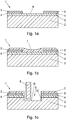
- a circuit board is denoted by 1, the circuit board 1 in the present case being an IMS circuit board (Insulated Metal Substrate).
- the IMS circuit board 1 is characterized by a relatively thick metal substrate 2, which can be made of copper or aluminum and can have a thickness of at least 50 ⁇ m up to a few millimeters.
- the substrate layer 2 is followed by an insulating layer 3, which as a rule consists of an insulating resin system filled with thermally conductive particles, for example epoxy resin.
- Conductor tracks 4 and gold surfaces 5, which serve as bonding surfaces, are arranged on this insulating layer 3.
- the circuit board 1 is thus ready to receive LED chips, which could be attached, for example, at the position 6, wherein the contacting of an LED chip could take place on the bonding surfaces 5.
- a temporary protective layer 7 is now applied to the circuit board 1 ( Figure 1b )) which covers the bonding surfaces 5.
- the temporary protective layer 7 could also cover the conductor tracks 4 made of copper if these were not covered by gold surfaces 5, as in the present case.
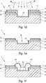
- Figure 1c it can now be seen that in accordance with Figure 1b ) preparatory circuit board, for example by means of a milling head 8, a cavity 9 can be produced. After this method step, the cavity 9 has cavity walls 10 which reflect relatively poorly. According to Fig.
- the reflector layer 11 is now applied, as is symbolized by the group of arrows 19. It can be seen that the reflector layer 11 covers both the temporary protective layer 7 and the cavity walls 10 over a large area. After removing the temporary protective layer 7 ( Fig. 1e )) a printed circuit board with a mirrored cavity 9 is now obtained, the reflector layer 11 only lining the interior of the cavity 9. An LED chip 12 can now be inserted into the mirrored cavity 9, which can be connected to the bonding surface 5 via bonding wires 13 ( Fig. 1f )).
- a circuit board 1 can again be seen, which, however, in the present case is not an IMS circuit board but a circuit board made of a well-known, glass fiber reinforced epoxy resin (eg FR4).
- the FR4 layer or prepreg layer is denoted here by 14, with copper layers 4 and bonding surfaces 5 again being present on the circuit board 1.
- a laser beam is symbolized by 15, which cuts both through the protective layer 7 and through the prepreg layer 14, which represents an insulating layer, until it strikes a laser stop layer 16, for example made of copper. With 17 an adhesion-reducing layer is designated, which facilitates the detachment of the plug 18 cut by means of the laser beam 15 ( Figure 2b )).
- the present invention can be used not only in conjunction with LED chips, but can also be useful for other optoelectronic components, such as, for example, for photodiodes or laser diodes, possibly together with a light conversion medium.
Landscapes
- Engineering & Computer Science (AREA)
- Microelectronics & Electronic Packaging (AREA)
- Manufacturing & Machinery (AREA)
- Physics & Mathematics (AREA)
- Optics & Photonics (AREA)
- Led Device Packages (AREA)
- Optical Elements Other Than Lenses (AREA)
- Manufacturing Of Printed Wiring (AREA)
Claims (17)
- Procédé de fabrication d'une carte de circuit imprimé comportant au moins une cavité destinée à recevoir un composant optoélectronique, les parois de la cavité présentant une couche réfléchissante, en particulier spéculaire, comportant les étapes suivantes :- fournir une carte de circuit imprimé (1),- appliquer une couche de protection temporaire (7) sur au moins une région partielle de la surface de la carte de circuit imprimé (1),- fournir à la cavité (9) une pénétration de la couche protectrice (7) dans la région de la cavité (9),- appliquer la couche réflectrice (11), la couche réflectrice (11) recouvrant la surface à la fois de la couche protectrice temporaire (7) et des parois de la cavité (10), et- enlever la couche de protection temporaire (7).
- Procédé selon la revendication 1, caractérisé en ce qu'une carte de circuit imprimé (1) avec des surfaces de liaison structurées (5) pour des composants électroniques (12) est fournie.
- Procédé selon la revendication 1 ou 2, caractérisé en ce qu'une carte de circuit imprimé IMS (1) est prévue comme carte de circuit imprimé (1).
- Procédé selon l'une quelconque des revendications 1 à 3, caractérisé en ce que l'étape de production de la cavité (9) comprend le fraisage de la carte de circuit imprimé (1) avec une tête de fraisage (8).
- Procédé selon la revendication 1 ou 2, caractérisé en ce qu'une carte de circuit imprimé (1) faite d'un matériau préimprégné est fournie comme carte de circuit imprimé (1).
- Procédé selon la revendication 5, caractérisé en ce que l'étape de production de la cavité (9) comprend la découpe de la carte de circuit imprimé (1) avec un faisceau laser (15).
- Procédé selon l'une des revendications 1 ou 2, caractérisé en ce que la carte de circuit imprimé (1) comprend une couche de réduction d'adhérence (17) disposée au-dessus d'une couche d'arrêt laser (16).
- Procédé selon l'une quelconque des revendications 1 à 7, caractérisé en ce qu'un film auto-adhésif est appliqué comme couche protectrice temporaire (7).
- Procédé selon la revendication 8, caractérisé en ce que le film auto-adhésif est un film à base de polyéthylène avec une couche adhésive à base de caoutchouc.
- Procédé selon la revendication 8, caractérisé en ce que le film auto-adhésif est un film à base de PVC avec une couche adhésive à base d'acrylate.
- Procédé selon la revendication 8, caractérisé en ce que le film auto-adhésif est un film à base de polyéthylène avec une couche adhésive à base d'acrylate.
- Procédé selon l'une quelconque des revendications 1 à 7, caractérisé en ce qu'un vernis à base de silicone est appliqué comme couche protectrice temporaire (7).
- Procédé selon l'une quelconque des revendications 1 à 12, caractérisé en ce que la couche réflectrice (11) est formée d'une laque choisie dans le groupe constitué par les laques époxy et les laques d'acrylate.
- Procédé selon l'une quelconque des revendications 1 à 12, caractérisé en ce que la couche de réflecteur (11) est appliquée sur la carte de circuit imprimé en tant que couche métallique des métaux choisis dans le groupe constitué par Al, Ag et Rh.
- Procédé selon la revendication 14, caractérisé en ce qu'on applique en plus une couche choisie dans le groupe constitué par l'oxyde de silicium et l'oxyde d'aluminium.
- Procédé selon l'une quelconque des revendications 1 à 12, caractérisé en ce que l'étape de cerclage de la couche réflectrice (11) comprend les étapes suivantes :- Peindre la cavité (9) avec une peinture brillante,- l'application d'une couche de métal réfléchissant sur la laque brillante,- l'application d'une couche protectrice à base d'hexaméthylsiloxane sur la couche réfléchissante
- Procédé selon l'une des revendications 1 à 16, caractérisé en ce que pendant l'étape de réalisation de la cavité (9), on maintient une distance par rapport aux pistes conductrices (4) ou aux surfaces de liaison (5) existantes de la carte de circuit imprimé (1).
Priority Applications (1)
| Application Number | Priority Date | Filing Date | Title |
|---|---|---|---|
| EP21179979.6A EP3902020A1 (fr) | 2014-01-29 | 2015-01-21 | Carte de circuit imprimé |
Applications Claiming Priority (2)
| Application Number | Priority Date | Filing Date | Title |
|---|---|---|---|
| ATA50058/2014A AT515372B1 (de) | 2014-01-29 | 2014-01-29 | Verfahren zur Herstellung einer Leiterplatte |
| PCT/AT2015/050019 WO2015113088A1 (fr) | 2014-01-29 | 2015-01-21 | Procédé de production d'une carte de circuits imprimés |
Related Child Applications (1)
| Application Number | Title | Priority Date | Filing Date |
|---|---|---|---|
| EP21179979.6A Division EP3902020A1 (fr) | 2014-01-29 | 2015-01-21 | Carte de circuit imprimé |
Publications (2)
| Publication Number | Publication Date |
|---|---|
| EP3100310A1 EP3100310A1 (fr) | 2016-12-07 |
| EP3100310B1 true EP3100310B1 (fr) | 2021-07-07 |
Family
ID=52633004
Family Applications (2)
| Application Number | Title | Priority Date | Filing Date |
|---|---|---|---|
| EP15708697.6A Active EP3100310B1 (fr) | 2014-01-29 | 2015-01-21 | Procédé de production d'une carte de circuits imprimés |
| EP21179979.6A Withdrawn EP3902020A1 (fr) | 2014-01-29 | 2015-01-21 | Carte de circuit imprimé |
Family Applications After (1)
| Application Number | Title | Priority Date | Filing Date |
|---|---|---|---|
| EP21179979.6A Withdrawn EP3902020A1 (fr) | 2014-01-29 | 2015-01-21 | Carte de circuit imprimé |
Country Status (5)
| Country | Link |
|---|---|
| US (1) | US9713248B2 (fr) |
| EP (2) | EP3100310B1 (fr) |
| CN (1) | CN106165131B (fr) |
| AT (1) | AT515372B1 (fr) |
| WO (1) | WO2015113088A1 (fr) |
Families Citing this family (12)
| Publication number | Priority date | Publication date | Assignee | Title |
|---|---|---|---|---|
| US10219384B2 (en) | 2013-11-27 | 2019-02-26 | At&S Austria Technologie & Systemtechnik Aktiengesellschaft | Circuit board structure |
| AT515101B1 (de) | 2013-12-12 | 2015-06-15 | Austria Tech & System Tech | Verfahren zum Einbetten einer Komponente in eine Leiterplatte |
| AT515372B1 (de) | 2014-01-29 | 2019-10-15 | At & S Austria Tech & Systemtechnik Ag | Verfahren zur Herstellung einer Leiterplatte |
| AT515447B1 (de) | 2014-02-27 | 2019-10-15 | At & S Austria Tech & Systemtechnik Ag | Verfahren zum Kontaktieren eines in eine Leiterplatte eingebetteten Bauelements sowie Leiterplatte |
| US11523520B2 (en) | 2014-02-27 | 2022-12-06 | At&S Austria Technologie & Systemtechnik Aktiengesellschaft | Method for making contact with a component embedded in a printed circuit board |
| US9918414B2 (en) * | 2015-12-18 | 2018-03-13 | Intel Corporation | Electromagnetic interference shields for electronic packages and related methods |
| CN109219255A (zh) * | 2018-11-14 | 2019-01-15 | 生益电子股份有限公司 | 一种非金属化阶梯槽的制作方法及pcb |
| CN112382206B (zh) | 2020-11-13 | 2022-07-12 | Tcl华星光电技术有限公司 | 背板及led面板 |
| EP4248717A2 (fr) | 2020-11-18 | 2023-09-27 | AT & S Austria Technologie & Systemtechnik Aktiengesellschaft | Support de composant pour applications de guide d'ondes |
| US11664567B2 (en) | 2020-11-30 | 2023-05-30 | Nxp B.V. | Hollow waveguide assembly formed by affixing first and second substrates to form a cavity therein and having a conductive layer covering the cavity |
| CN115707194A (zh) | 2021-08-04 | 2023-02-17 | 奥特斯奥地利科技与系统技术有限公司 | 部件承载件及其制造方法 |
| CN114928947A (zh) * | 2022-05-31 | 2022-08-19 | 景旺电子科技(龙川)有限公司 | Oled模组刚挠结合板制作方法及刚挠结合板 |
Family Cites Families (20)
| Publication number | Priority date | Publication date | Assignee | Title |
|---|---|---|---|---|
| US5206188A (en) * | 1990-01-31 | 1993-04-27 | Ibiden Co., Ltd. | Method of manufacturing a high lead count circuit board |
| JP3736679B2 (ja) * | 2001-07-18 | 2006-01-18 | 日立エーアイシー株式会社 | プリント配線板 |
| JP2004200209A (ja) * | 2002-12-16 | 2004-07-15 | Fuji Xerox Co Ltd | 電極等の導電パターンの形成方法およびこれを用いた面発光型半導体レーザ並びにその製造方法 |
| TWI312583B (en) * | 2004-03-18 | 2009-07-21 | Phoseon Technology Inc | Micro-reflectors on a substrate for high-density led array |
| JP4659421B2 (ja) * | 2004-09-30 | 2011-03-30 | 株式会社トクヤマ | 発光素子収納用パッケージの製造方法 |
| KR20060106891A (ko) * | 2005-04-04 | 2006-10-12 | 마츠시타 덴끼 산교 가부시키가이샤 | 광학 디바이스용 캐비티 구조체, 광학 디바이스 및 광학디바이스용 캐비티 구조체의 제조방법 |
| CN1901238A (zh) * | 2005-07-20 | 2007-01-24 | 桦晶科技股份有限公司 | 发光二极管(led)无打线的封装结构 |
| JP4771135B2 (ja) | 2006-01-12 | 2011-09-14 | 日立化成工業株式会社 | プリント配線板、それを使用したled装置及びプリント配線板の製造方法 |
| KR100782798B1 (ko) * | 2006-02-22 | 2007-12-05 | 삼성전기주식회사 | 기판 패키지 및 그 제조 방법 |
| CN101093828A (zh) * | 2006-06-20 | 2007-12-26 | 常州东村电子有限公司 | 紧凑型大功率发光二极管的封装结构 |
| JP2008166736A (ja) * | 2006-12-06 | 2008-07-17 | Hitachi Via Mechanics Ltd | プリント基板の製造方法およびプリント基板加工機 |
| JP2009021426A (ja) * | 2007-07-12 | 2009-01-29 | Sharp Corp | チップ部品型led及びその製造方法 |
| KR20090104580A (ko) * | 2008-03-31 | 2009-10-06 | 서울반도체 주식회사 | 인쇄 회로 기판을 이용한 발광 다이오드 패키지 |
| AT12322U1 (de) | 2009-01-27 | 2012-03-15 | Dcc Dev Circuits & Components Gmbh | Verfahren zur herstellung einer mehrlagigen leiterplatte, haftverhinderungsmaterial sowie mehrlagige leiterplatte und verwendung eines derartigen verfahrens |
| TWM390542U (en) * | 2010-03-17 | 2010-10-11 | Hon Hai Prec Ind Co Ltd | LED lead frame |
| JP2012044102A (ja) | 2010-08-23 | 2012-03-01 | Hitachi Cable Ltd | 発光装置及びその製造方法並びに配線基板 |
| KR101883839B1 (ko) * | 2010-12-07 | 2018-08-30 | 엘지이노텍 주식회사 | 발광소자 모듈 및 이를 포함하는 백라이트 유닛 |
| AT13434U1 (de) * | 2012-02-21 | 2013-12-15 | Austria Tech & System Tech | Verfahren zur Herstellung einer Leiterplatte und Verwendung eines derartigen Verfahrens |
| KR20130106967A (ko) * | 2012-03-21 | 2013-10-01 | 엘지이노텍 주식회사 | 인쇄회로기판 및 그 제조방법 |
| AT515372B1 (de) | 2014-01-29 | 2019-10-15 | At & S Austria Tech & Systemtechnik Ag | Verfahren zur Herstellung einer Leiterplatte |
-
2014
- 2014-01-29 AT ATA50058/2014A patent/AT515372B1/de not_active IP Right Cessation
-
2015
- 2015-01-21 US US15/115,221 patent/US9713248B2/en not_active Expired - Fee Related
- 2015-01-21 EP EP15708697.6A patent/EP3100310B1/fr active Active
- 2015-01-21 WO PCT/AT2015/050019 patent/WO2015113088A1/fr not_active Ceased
- 2015-01-21 CN CN201580016774.6A patent/CN106165131B/zh active Active
- 2015-01-21 EP EP21179979.6A patent/EP3902020A1/fr not_active Withdrawn
Non-Patent Citations (1)
| Title |
|---|
| None * |
Also Published As
| Publication number | Publication date |
|---|---|
| US20160353566A1 (en) | 2016-12-01 |
| EP3902020A1 (fr) | 2021-10-27 |
| US9713248B2 (en) | 2017-07-18 |
| EP3100310A1 (fr) | 2016-12-07 |
| AT515372A1 (de) | 2015-08-15 |
| CN106165131B (zh) | 2019-04-26 |
| CN106165131A (zh) | 2016-11-23 |
| AT515372B1 (de) | 2019-10-15 |
| WO2015113088A1 (fr) | 2015-08-06 |
Similar Documents
| Publication | Publication Date | Title |
|---|---|---|
| EP3100310B1 (fr) | Procédé de production d'une carte de circuits imprimés | |
| DE112013007310B4 (de) | Eine metallische Platinenstruktur für das Packaging vor dem Ätzen von 3D-System-In-Package Flip-Chips und ein dafür geeignetes Verfahren | |
| DE102011011139B4 (de) | Verfahren zur Herstellung zumindest eines optoelektronischen Halbleiterbauelements und optoelektronisches Halbleiterbauelement | |
| EP2606510B1 (fr) | Procédé de fabrication d'au moins un composant semi-conducteur optoélectronique | |
| EP1269450B1 (fr) | Composant pourvu d'une inscription | |
| EP1685603A2 (fr) | Technique de connexion et de fabrication miniaturisee et a couts reduits pour des dels et d'autres modules optoelectroniques | |
| WO2007121737A1 (fr) | Élément avec marquage optique, procédé de fabrication et utilisation | |
| DE102004020204A1 (de) | Verkapseltes elektrisches Bauelement und Verfahren zur Herstellung | |
| WO2014072256A1 (fr) | Composant à semi-conducteur optoélectronique | |
| US20150342062A1 (en) | Semi-Finished Product for the Production of a Printed Circuit Board, Method for Producing a Printed Circuit Board and Printed Circuit Board | |
| DE102013212247B4 (de) | Optoelektronisches Bauelement und Verfahren zu seiner Herstellung | |
| EP2425688A1 (fr) | Procédé de fabrication d'une carte de circuit imprimé comportant des diodes électroluminescentes et une surface réfléchissante imprimée, et carte de circuit imprimé fabriquée selon le procédé | |
| EP3026702B1 (fr) | Procede de fabrication d'un element semi-conducteur dote d'un adaptateur de substrat et element semi-conducteur dote d'un adaptateur de substrat | |
| DE102017220258B4 (de) | Halbleitersensorbauelement und Verfahren zum Herstellen desselben | |
| DE102019115600A1 (de) | Bauelement mit korrosionsschutz und verfahren zur herstellung eines bauelements mit korrosionsschutz | |
| EP2982226B1 (fr) | Procédé de fabrication d'un élément de circuit imprimé | |
| DE102016103819A1 (de) | Anschlussträger, optoelektronisches Bauteil und Verfahren zur Herstellung eines Anschlussträgers oder eines optoelektronischen Bauteils | |
| WO2017194620A1 (fr) | Composant optoélectronique et procédé de fabrication d'un composant optoélectronique | |
| DE102014112365A1 (de) | Verfahren zur Herstellung eines Mehrschichtsubstrats und Mehrschichtsubstrat | |
| DE102009040176B4 (de) | Halbleiter-Bauelement und Verfahren zum Herstellen eines Halbleiterbauelements | |
| DE10250911B4 (de) | Verfahren zur Herstellung einer Umhüllung und/oder zumindest eines Teiles eines Gehäuses eines optoelektronischen Bauelements | |
| DE102014110971A1 (de) | Optoelektronisches Bauelement und Verfahren zur Herstellung eines optoelektronischen Bauelements | |
| EP3123842A1 (fr) | Couche adhérente sur céramique et/ou masque anti-soudure, en tant que vernis de protection ou masse de scellement | |
| WO2013139493A1 (fr) | Plaque de recouvrement, module optoélectronique à semi-conducteurs et procédé de fabrication d'un module optoélectronique à semi-conducteurs | |
| DE2105550A1 (de) | Verfahren zum Herstellen eines Halbleiterbauelementes |
Legal Events
| Date | Code | Title | Description |
|---|---|---|---|
| PUAI | Public reference made under article 153(3) epc to a published international application that has entered the european phase |
Free format text: ORIGINAL CODE: 0009012 |
|
| STAA | Information on the status of an ep patent application or granted ep patent |
Free format text: STATUS: REQUEST FOR EXAMINATION WAS MADE |
|
| 17P | Request for examination filed |
Effective date: 20160815 |
|
| AK | Designated contracting states |
Kind code of ref document: A1 Designated state(s): AL AT BE BG CH CY CZ DE DK EE ES FI FR GB GR HR HU IE IS IT LI LT LU LV MC MK MT NL NO PL PT RO RS SE SI SK SM TR |
|
| AX | Request for extension of the european patent |
Extension state: BA ME |
|
| DAX | Request for extension of the european patent (deleted) | ||
| STAA | Information on the status of an ep patent application or granted ep patent |
Free format text: STATUS: EXAMINATION IS IN PROGRESS |
|
| 17Q | First examination report despatched |
Effective date: 20200921 |
|
| GRAP | Despatch of communication of intention to grant a patent |
Free format text: ORIGINAL CODE: EPIDOSNIGR1 |
|
| STAA | Information on the status of an ep patent application or granted ep patent |
Free format text: STATUS: GRANT OF PATENT IS INTENDED |
|
| RIC1 | Information provided on ipc code assigned before grant |
Ipc: H01L 33/60 20100101AFI20210118BHEP Ipc: H05K 3/00 20060101ALI20210118BHEP Ipc: H01L 33/62 20100101ALI20210118BHEP Ipc: H05K 1/18 20060101ALI20210118BHEP |
|
| INTG | Intention to grant announced |
Effective date: 20210210 |
|
| GRAS | Grant fee paid |
Free format text: ORIGINAL CODE: EPIDOSNIGR3 |
|
| GRAA | (expected) grant |
Free format text: ORIGINAL CODE: 0009210 |
|
| STAA | Information on the status of an ep patent application or granted ep patent |
Free format text: STATUS: THE PATENT HAS BEEN GRANTED |
|
| AK | Designated contracting states |
Kind code of ref document: B1 Designated state(s): AL AT BE BG CH CY CZ DE DK EE ES FI FR GB GR HR HU IE IS IT LI LT LU LV MC MK MT NL NO PL PT RO RS SE SI SK SM TR |
|
| REG | Reference to a national code |
Ref country code: GB Ref legal event code: FG4D Free format text: NOT ENGLISH |
|
| REG | Reference to a national code |
Ref country code: AT Ref legal event code: REF Ref document number: 1409437 Country of ref document: AT Kind code of ref document: T Effective date: 20210715 |
|
| REG | Reference to a national code |
Ref country code: DE Ref legal event code: R096 Ref document number: 502015014907 Country of ref document: DE |
|
| REG | Reference to a national code |
Ref country code: IE Ref legal event code: FG4D Free format text: LANGUAGE OF EP DOCUMENT: GERMAN |
|
| REG | Reference to a national code |
Ref country code: LT Ref legal event code: MG9D |
|
| REG | Reference to a national code |
Ref country code: NL Ref legal event code: MP Effective date: 20210707 |
|
| PG25 | Lapsed in a contracting state [announced via postgrant information from national office to epo] |
Ref country code: LT Free format text: LAPSE BECAUSE OF FAILURE TO SUBMIT A TRANSLATION OF THE DESCRIPTION OR TO PAY THE FEE WITHIN THE PRESCRIBED TIME-LIMIT Effective date: 20210707 Ref country code: BG Free format text: LAPSE BECAUSE OF FAILURE TO SUBMIT A TRANSLATION OF THE DESCRIPTION OR TO PAY THE FEE WITHIN THE PRESCRIBED TIME-LIMIT Effective date: 20211007 Ref country code: ES Free format text: LAPSE BECAUSE OF FAILURE TO SUBMIT A TRANSLATION OF THE DESCRIPTION OR TO PAY THE FEE WITHIN THE PRESCRIBED TIME-LIMIT Effective date: 20210707 Ref country code: FI Free format text: LAPSE BECAUSE OF FAILURE TO SUBMIT A TRANSLATION OF THE DESCRIPTION OR TO PAY THE FEE WITHIN THE PRESCRIBED TIME-LIMIT Effective date: 20210707 Ref country code: NL Free format text: LAPSE BECAUSE OF FAILURE TO SUBMIT A TRANSLATION OF THE DESCRIPTION OR TO PAY THE FEE WITHIN THE PRESCRIBED TIME-LIMIT Effective date: 20210707 Ref country code: PT Free format text: LAPSE BECAUSE OF FAILURE TO SUBMIT A TRANSLATION OF THE DESCRIPTION OR TO PAY THE FEE WITHIN THE PRESCRIBED TIME-LIMIT Effective date: 20211108 Ref country code: NO Free format text: LAPSE BECAUSE OF FAILURE TO SUBMIT A TRANSLATION OF THE DESCRIPTION OR TO PAY THE FEE WITHIN THE PRESCRIBED TIME-LIMIT Effective date: 20211007 Ref country code: SE Free format text: LAPSE BECAUSE OF FAILURE TO SUBMIT A TRANSLATION OF THE DESCRIPTION OR TO PAY THE FEE WITHIN THE PRESCRIBED TIME-LIMIT Effective date: 20210707 Ref country code: RS Free format text: LAPSE BECAUSE OF FAILURE TO SUBMIT A TRANSLATION OF THE DESCRIPTION OR TO PAY THE FEE WITHIN THE PRESCRIBED TIME-LIMIT Effective date: 20210707 Ref country code: HR Free format text: LAPSE BECAUSE OF FAILURE TO SUBMIT A TRANSLATION OF THE DESCRIPTION OR TO PAY THE FEE WITHIN THE PRESCRIBED TIME-LIMIT Effective date: 20210707 |
|
| PG25 | Lapsed in a contracting state [announced via postgrant information from national office to epo] |
Ref country code: PL Free format text: LAPSE BECAUSE OF FAILURE TO SUBMIT A TRANSLATION OF THE DESCRIPTION OR TO PAY THE FEE WITHIN THE PRESCRIBED TIME-LIMIT Effective date: 20210707 Ref country code: LV Free format text: LAPSE BECAUSE OF FAILURE TO SUBMIT A TRANSLATION OF THE DESCRIPTION OR TO PAY THE FEE WITHIN THE PRESCRIBED TIME-LIMIT Effective date: 20210707 Ref country code: GR Free format text: LAPSE BECAUSE OF FAILURE TO SUBMIT A TRANSLATION OF THE DESCRIPTION OR TO PAY THE FEE WITHIN THE PRESCRIBED TIME-LIMIT Effective date: 20211008 |
|
| REG | Reference to a national code |
Ref country code: DE Ref legal event code: R097 Ref document number: 502015014907 Country of ref document: DE |
|
| PG25 | Lapsed in a contracting state [announced via postgrant information from national office to epo] |
Ref country code: DK Free format text: LAPSE BECAUSE OF FAILURE TO SUBMIT A TRANSLATION OF THE DESCRIPTION OR TO PAY THE FEE WITHIN THE PRESCRIBED TIME-LIMIT Effective date: 20210707 |
|
| PLBE | No opposition filed within time limit |
Free format text: ORIGINAL CODE: 0009261 |
|
| STAA | Information on the status of an ep patent application or granted ep patent |
Free format text: STATUS: NO OPPOSITION FILED WITHIN TIME LIMIT |
|
| PG25 | Lapsed in a contracting state [announced via postgrant information from national office to epo] |
Ref country code: SM Free format text: LAPSE BECAUSE OF FAILURE TO SUBMIT A TRANSLATION OF THE DESCRIPTION OR TO PAY THE FEE WITHIN THE PRESCRIBED TIME-LIMIT Effective date: 20210707 Ref country code: SK Free format text: LAPSE BECAUSE OF FAILURE TO SUBMIT A TRANSLATION OF THE DESCRIPTION OR TO PAY THE FEE WITHIN THE PRESCRIBED TIME-LIMIT Effective date: 20210707 Ref country code: RO Free format text: LAPSE BECAUSE OF FAILURE TO SUBMIT A TRANSLATION OF THE DESCRIPTION OR TO PAY THE FEE WITHIN THE PRESCRIBED TIME-LIMIT Effective date: 20210707 Ref country code: EE Free format text: LAPSE BECAUSE OF FAILURE TO SUBMIT A TRANSLATION OF THE DESCRIPTION OR TO PAY THE FEE WITHIN THE PRESCRIBED TIME-LIMIT Effective date: 20210707 Ref country code: CZ Free format text: LAPSE BECAUSE OF FAILURE TO SUBMIT A TRANSLATION OF THE DESCRIPTION OR TO PAY THE FEE WITHIN THE PRESCRIBED TIME-LIMIT Effective date: 20210707 Ref country code: AL Free format text: LAPSE BECAUSE OF FAILURE TO SUBMIT A TRANSLATION OF THE DESCRIPTION OR TO PAY THE FEE WITHIN THE PRESCRIBED TIME-LIMIT Effective date: 20210707 |
|
| 26N | No opposition filed |
Effective date: 20220408 |
|
| PG25 | Lapsed in a contracting state [announced via postgrant information from national office to epo] |
Ref country code: IT Free format text: LAPSE BECAUSE OF FAILURE TO SUBMIT A TRANSLATION OF THE DESCRIPTION OR TO PAY THE FEE WITHIN THE PRESCRIBED TIME-LIMIT Effective date: 20210707 |
|
| PG25 | Lapsed in a contracting state [announced via postgrant information from national office to epo] |
Ref country code: MC Free format text: LAPSE BECAUSE OF FAILURE TO SUBMIT A TRANSLATION OF THE DESCRIPTION OR TO PAY THE FEE WITHIN THE PRESCRIBED TIME-LIMIT Effective date: 20210707 |
|
| REG | Reference to a national code |
Ref country code: CH Ref legal event code: PL |
|
| GBPC | Gb: european patent ceased through non-payment of renewal fee |
Effective date: 20220121 |
|
| REG | Reference to a national code |
Ref country code: BE Ref legal event code: MM Effective date: 20220131 |
|
| PG25 | Lapsed in a contracting state [announced via postgrant information from national office to epo] |
Ref country code: LU Free format text: LAPSE BECAUSE OF NON-PAYMENT OF DUE FEES Effective date: 20220121 Ref country code: GB Free format text: LAPSE BECAUSE OF NON-PAYMENT OF DUE FEES Effective date: 20220121 |
|
| PG25 | Lapsed in a contracting state [announced via postgrant information from national office to epo] |
Ref country code: BE Free format text: LAPSE BECAUSE OF NON-PAYMENT OF DUE FEES Effective date: 20220131 |
|
| PG25 | Lapsed in a contracting state [announced via postgrant information from national office to epo] |
Ref country code: LI Free format text: LAPSE BECAUSE OF NON-PAYMENT OF DUE FEES Effective date: 20220131 Ref country code: CH Free format text: LAPSE BECAUSE OF NON-PAYMENT OF DUE FEES Effective date: 20220131 |
|
| PG25 | Lapsed in a contracting state [announced via postgrant information from national office to epo] |
Ref country code: IE Free format text: LAPSE BECAUSE OF NON-PAYMENT OF DUE FEES Effective date: 20220121 |
|
| REG | Reference to a national code |
Ref country code: AT Ref legal event code: MM01 Ref document number: 1409437 Country of ref document: AT Kind code of ref document: T Effective date: 20220121 |
|
| PG25 | Lapsed in a contracting state [announced via postgrant information from national office to epo] |
Ref country code: AT Free format text: LAPSE BECAUSE OF NON-PAYMENT OF DUE FEES Effective date: 20220121 |
|
| P01 | Opt-out of the competence of the unified patent court (upc) registered |
Effective date: 20230526 |
|
| PG25 | Lapsed in a contracting state [announced via postgrant information from national office to epo] |
Ref country code: HU Free format text: LAPSE BECAUSE OF FAILURE TO SUBMIT A TRANSLATION OF THE DESCRIPTION OR TO PAY THE FEE WITHIN THE PRESCRIBED TIME-LIMIT; INVALID AB INITIO Effective date: 20150121 |
|
| PG25 | Lapsed in a contracting state [announced via postgrant information from national office to epo] |
Ref country code: MK Free format text: LAPSE BECAUSE OF FAILURE TO SUBMIT A TRANSLATION OF THE DESCRIPTION OR TO PAY THE FEE WITHIN THE PRESCRIBED TIME-LIMIT Effective date: 20210707 Ref country code: CY Free format text: LAPSE BECAUSE OF FAILURE TO SUBMIT A TRANSLATION OF THE DESCRIPTION OR TO PAY THE FEE WITHIN THE PRESCRIBED TIME-LIMIT Effective date: 20210707 |
|
| PG25 | Lapsed in a contracting state [announced via postgrant information from national office to epo] |
Ref country code: TR Free format text: LAPSE BECAUSE OF FAILURE TO SUBMIT A TRANSLATION OF THE DESCRIPTION OR TO PAY THE FEE WITHIN THE PRESCRIBED TIME-LIMIT Effective date: 20210707 |
|
| PG25 | Lapsed in a contracting state [announced via postgrant information from national office to epo] |
Ref country code: MT Free format text: LAPSE BECAUSE OF FAILURE TO SUBMIT A TRANSLATION OF THE DESCRIPTION OR TO PAY THE FEE WITHIN THE PRESCRIBED TIME-LIMIT Effective date: 20210707 |
|
| REG | Reference to a national code |
Ref country code: DE Ref legal event code: R079 Ref document number: 502015014907 Country of ref document: DE Free format text: PREVIOUS MAIN CLASS: H01L0033600000 Ipc: H10H0020856000 |
|
| PGFP | Annual fee paid to national office [announced via postgrant information from national office to epo] |
Ref country code: DE Payment date: 20260116 Year of fee payment: 12 |
|
| PGFP | Annual fee paid to national office [announced via postgrant information from national office to epo] |
Ref country code: FR Payment date: 20260126 Year of fee payment: 12 |