EP3101687A1 - Procédé de formation de boîtier et boîtier mems - Google Patents
Procédé de formation de boîtier et boîtier mems Download PDFInfo
- Publication number
- EP3101687A1 EP3101687A1 EP15740967.3A EP15740967A EP3101687A1 EP 3101687 A1 EP3101687 A1 EP 3101687A1 EP 15740967 A EP15740967 A EP 15740967A EP 3101687 A1 EP3101687 A1 EP 3101687A1
- Authority
- EP
- European Patent Office
- Prior art keywords
- thin film
- metal thin
- substrate
- sealing frame
- package
- Prior art date
- Legal status (The legal status is an assumption and is not a legal conclusion. Google has not performed a legal analysis and makes no representation as to the accuracy of the status listed.)
- Granted
Links
Images


Classifications
-
- B—PERFORMING OPERATIONS; TRANSPORTING
- B81—MICROSTRUCTURAL TECHNOLOGY
- B81C—PROCESSES OR APPARATUS SPECIALLY ADAPTED FOR THE MANUFACTURE OR TREATMENT OF MICROSTRUCTURAL DEVICES OR SYSTEMS
- B81C1/00—Manufacture or treatment of devices or systems in or on a substrate
- B81C1/00015—Manufacture or treatment of devices or systems in or on a substrate for manufacturing microsystems
- B81C1/00261—Processes for packaging MEMS devices
- B81C1/00269—Bonding of solid lids or wafers to the substrate
-
- B—PERFORMING OPERATIONS; TRANSPORTING
- B81—MICROSTRUCTURAL TECHNOLOGY
- B81C—PROCESSES OR APPARATUS SPECIALLY ADAPTED FOR THE MANUFACTURE OR TREATMENT OF MICROSTRUCTURAL DEVICES OR SYSTEMS
- B81C2203/00—Forming microstructural systems
- B81C2203/01—Packaging MEMS
- B81C2203/0118—Bonding a wafer on the substrate, i.e. where the cap consists of another wafer
-
- B—PERFORMING OPERATIONS; TRANSPORTING
- B81—MICROSTRUCTURAL TECHNOLOGY
- B81C—PROCESSES OR APPARATUS SPECIALLY ADAPTED FOR THE MANUFACTURE OR TREATMENT OF MICROSTRUCTURAL DEVICES OR SYSTEMS
- B81C2203/00—Forming microstructural systems
- B81C2203/01—Packaging MEMS
- B81C2203/0172—Seals
- B81C2203/019—Seals characterised by the material or arrangement of seals between parts
-
- B—PERFORMING OPERATIONS; TRANSPORTING
- B81—MICROSTRUCTURAL TECHNOLOGY
- B81C—PROCESSES OR APPARATUS SPECIALLY ADAPTED FOR THE MANUFACTURE OR TREATMENT OF MICROSTRUCTURAL DEVICES OR SYSTEMS
- B81C2203/00—Forming microstructural systems
- B81C2203/03—Bonding two components
- B81C2203/033—Thermal bonding
- B81C2203/035—Soldering
Definitions
- Our invention relates to a package for hollow-sealing of elements and a formation method thereof, and particularly relates to a package suitable for accommodating a precision mechanism such as Micro Electro Mechanical System (MEMS) in a hollow-sealed interior space and a formation method thereof.
- MEMS Micro Electro Mechanical System
- a Micro Electro Mechanical System (MEMS) of mechanical elements combined with electronic circuit elements is provided with a hollow package to physically protect fine moving part from external environments.
- a package may be formed by a known method in which a sealing substrate provided with a sealing frame (sealing pattern) or a bump electrode having a height of some ⁇ m to dozens ⁇ m are formed by metal plating and bonded onto a MEMS substrate by thermocompression.
- the metal constituting the sealing frame or bump electrode is often made of gold (Au) which is excellent in workability as well as physical characteristics such as high electric conductivity, high deformability and high corrosion resistance.
- Patent document 1 discloses package formation methods with their advantages and disadvantages, and discloses a method to bond them with a bonding material by thermocompression performed at a temperature lower than the melting temperature of the bonding material to soften without generating liquid phase. This method allegedly makes it possible to perform the thermocompression at a relatively low pressure while not requiring a process in which the bonded surface is highly smoothed (to lower roughness) or is deoxygenated by highly cleaned with extreme purity.
- the material for bonding the interface may be unalloyed metal such as Au, Sn, Cu and Al, a single phase of alloy such as AuSn, Au 5 Sn and AuIn, or mixture thereof.
- Non-patent document 1 discloses a package formation method, in which a predetermined sealing frame is formed by photoresist development on titanium-sputtered thin film having thickness of 50nm and gold-sputtered thin film having thickness of 200nm formed on wafers made of silicon or glass and then a sealing material made of gold particles is provided on the sealing frame by using a screen mask to perform thermocompression between the wafers.
- the two wafers are heated to 300°C in a vacuum chamber and then are bonded together at pushing pressure of 73MPa for 30min.
- the pushing pressure can be decreased by the sealing material made of gold particles, which is porous and easily deformed at the time of bonding.
- Non-patent document 2 discloses a low-temperature bonding method, in which gold stud bumps are formed on a gold thin film of silicon substrate and are subject to a coining with silicon chip to make the gold bump have a smooth top face to be activated with nitrogen atmosphere plasma and then bonded onto a gold thin film electrode having a surface activated by the same method as the top face.
- the bumps are heated to 150°C and bonded at pushing pressure of 320MPa for about 30sec. In the coining process, when the tip of bump is sharpened the smooth top face can be formed even at a low temperature and low pushing pressure.
- Patent Document 1 JP2012-009862-A
- thermocompression would require heating and pressurization to enhance adhesiveness at the bonding interface, so that the bonding interface is deformed.
- the heating might deform or destroy the substrate due to a generating of thermal stress in the junction between different kinds of materials on the substrate. That might cause even deterioration of device characteristics or alignment precision. Further, required time for such a process might become relatively long.
- MEMS Micro Electro Mechanical Systems
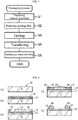
- Our invention is a package formation method for housing a precision machine element on a machine substrate in a hollow-sealed interior space, comprising: a sacrificial thin film formation step to perform a chemical-mechanical polishing with a temporary substrate made of an easily polishable material and sputter a metal thin film on the smoothly polished surface; a first bonding step to form a sealing frame by bringing at least a noble metal on the metal thin film and bond a substrate with the sealing frame; a temporary substrate removal step to remove the metal thin film together with the temporary substrate and expose a newborn face at a tip of the sealing frame; and a second bonding step to form a noble metal thin film around the precision machine element on the machine substrate, bring the newborn face of the sealing frame into contact onto the noble metal thin film, and join the newborn face of the sealing frame onto the noble metal thin film at room temperature.
- a newborn smooth noble metal face can easily be formed by transferring the smooth face of temporary substrate on an end face of sealing frame and can be bonded with a noble metal smooth face of machine substrate at room temperature.
- a package can be made suitable for housing a precision mechanism (machine element) such as a Micro Electro Mechanical Systems in a hollow-sealed interior space, without requiring any excessive heating and pressurization.
- the first bonding step includes a step to form the sealing frame by a plating method
- the sacrificial thin film formation step includes a step to form a seed metal thin film made of a noble metal on the metal thin film made of titanium or chrome.
- the noble metal constituting the seed metal thin film is gold.
- the second bonding step includes a step to activate bonding surfaces by plasma ashing.
- the bonding at the room temperature is performed at 200°C or less.
- a package can be made further suitable for housing a precision mechanism such as a Micro Electro Mechanical System in a hollow-sealed interior space while the machine substrate can be prevented from deforming thermally.
- a MEMS package formed by the package formation method described above is characterized by being capable of maintaining an interior vacuum condition of 10 -4 Pa at least for 6 months. With such a package, operations of MEMS inside the hollow-sealed interior space can be maintained for a long term.
- super smooth face 1a in terms of nanometer order is formed on substrate 1 made of material polishable easily.
- super smooth face 1a is formed on substrate 1 polished by CMP (Chemical Mechanical Polishing) or the like to be smoothed at the atomic level with high precision. It is preferable that easily polishable material such as Si, sapphire, quartz and glass is used as substrate 1, because substrate 1 doesn't remain in the final package structure (cf. Fig. 4(b) ) as described later and therefore material of the package is not limited thereto.
- sacrificial thin film 11 having thickness around some ten nm is formed by sputtering, such as vapor deposition and ion beam sputtering, on super smooth face 1a of substrate 1.
- Sacrificial thin film 11 having a smooth top face transferred from super smooth face 1a of substrate 1 should be thinner to the extent maintaining functions of transferring super smooth face 1a as a thin film without generating island or pinhole.
- sacrificial thin film 11 should have desirable material and thickness so that seed thin film 12 and plating film 14 hardly react on the sacrificial thin film and are easily peeled from the sacrificial thin film.
- sacrificial thin film 11 is made of Cr which is etched with properly-selected etchant.
- Seed thin film 12 providing an electrodeposition face of plating film 14 is formed by sputtering on sacrificial thin film 11.
- Seed thin film 12 may be made of a conductive noble metal such as Au.
- resist 13 is formed in the reversed pattern of a desirable sealing frame on sacrificial thin film 11. Then as shown in Fig. 2(d) , plating film 14 made of noble metal is formed through a window of resist 13 on seed thin film 12.
- Plating film 14 is typically an Au plating film made by electrolytic plating. Seed thin film 12 may be omitted when plating film 14 is formed directly on conductive sacrificial thin film 11.
- resist 13 is dissolved with acetone while seed thin film 12 except a portion below plating film 14 is removed with predetermined solution or gas.
- a sealing frame pattern comprising plating film 14 and seed thin film 12 between sacrificial thin film 11 and plating film 14 is formed on substrate 1.
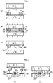
- sealing substrate 21 made of Si having a face of metal thin film 14' made of Au is placed on the side of plating film 14 on substrate 1. Then as shown in Fig. 3(b) , they are compressed with each other as being heated. It is possible that metal thin film 14' is formed all over the face sealing substrate 21 or is formed as corresponding to the sealing frame pattern.
- sacrificial film 11 is selectively etched chemically without etching seed thin film 12 and plating film 14 to form sealing cover 14a integrating seed thin film 12 and plating film 14 on substrate 1 and metal thin film 14' on sealing substrate 21. Then, a smooth top face of sacrificial film 11, namely a newborn smooth face made by transferring super smooth face 1a of substrate 1, appears on tip face 14a1 of wall portion of sealing cover 14a.
- a surface as smooth as super smooth face 1a of substrate 1 is formed on MEMS substrate 31 provided with MEMS device 31a, and then metal thin film 31b made of Au or the like is formed on it. It is possible that metal thin film 31b is formed all over MEMS substrate 31 or is formed as corresponding to the sealing frame pattern. An adhesion layer not shown or the like may be provided between MEMS substrate 31 and metal thin film 31b.
- Tip face 14a1 of sealing cover 14a and metal thin film 31b are activated on the surface where organics or the like on the surface have been removed by plasma ashing with oxygen or argon.
- sealing substrate 21 and MEMS board 31 faced to each other are held at a temperature of 200°C or less, so that activated surfaces of tip face 14a1 of sealing cover 14a and metal thin film 31b are put together with metal bonding to prepare a strong package structure having sealing wall 14b integrated.
- the above-described packaging process can be performed at lower temperature and lower pressure than conventional methods, and can save cost and prevent the operation reliability of MEMS devices including precision mechanism from being violated.
- sealing wall 14b (cf. Fig. 4 ) has metal junction 14d made of Au between activated surfaces as well as another part 14c made of another material.
- plating film 14 made of another material other than Au is formed directly on seed thin film made of Au, or another material is applied onto seed thin film 12 through a window of resist 13. With such a configuration, the amount of use of expensive Au can be suppressed to reduce a material cost.
- Fig. 6 shows results of measurement of surface roughness on tip face 14a1 of wall portion of sealing cover 14a with an atomic force microscope.
- substrate 1 made of Si is polished with abrasive grains made of colloidal silica to make super smooth face 1a, to which sacrificial thin film 11 made of Ti is applied by 30nm thickness, seed thin film 12 made of Au is further applied by 50nm thickness and plating film 14 made of Au is further applied by 10 ⁇ m thickness. Leaving seed thin film 12, only sacrificial thin film 11 is selectively etched chemically with 10% HF. Thus obtained part corresponding to tip face 14a1 of wall portion of sealing cover 14a is observed with an atomic force microscope to measure a surface roughness.
- Fig. 6(a) shows results of measuring a range of 3 ⁇ m square. It shows Sq of 0.84nm, representing excellent smoothness.
- Super smooth face 1a has Sq of 0.2nm while sacrificial layer thin film 11 has Sq of 0.6nm.
- Fig. 6(b) shows results of measuring the surface of plating film 14 on seed thin film 12, formed on ordinary substrate 1 made of Si. It shows surface roughness Sq of 16.2nm, representing poor smoothness greatly worse than the Example.
- sealing substrate 21 and MEMS substrate 31 are evaluated through tensile test.
- a sample of 3mm square frame (width 0.1mm) is prepared similarly to the one used for the smoothness evaluation and is bonded with a substrate imitating substrate 31 to prepare a test piece for tensile test. It is set to an Instron type tension tester (made by Shimadzu Corporation; AGS-10kN to measure a bonding strength at tensile speed of 0.5 [mm/min].
- the average breaking strength is 318N, representing almost the same level of bonding strength as the case of thermocompression between sealing substrate 21 and MEMS substrate 31.
- Comparative Example with a tensile test piece of Au-plated ordinary Si substrate shows 33N of average strength as only 1/10 times as the strength above.
- An airtight sealing performance of a whole package is evaluated with SOI (Silicon On Insulator) substrate as a sealing substrate.
- SOI Silicon On Insulator
- the airtight sealing performance of a whole package can be evaluated by measuring a temporal change of elastic deformation generated in membrane portion 21' when interior space is vacuumed in SOI substrate 21 having thin membrane portion 21' having thickness around 10 ⁇ m which is supported by a peripheral support.
- Support of SOI substrate 21 and MEMS substrate (Si substrate) 31 are respectively provided with sealing frame 14a and metal thin film 31b. Their surfaces are activated with argon plasma like the above described Example and bonded together in a vacuum, and then are kept in the atmosphere.
- the package is highly airtight as a whole the vacuum of the interior space is maintained and dent deformation generated in membrane portion 21' doesn't change with time.
- the difference between exterior atmosphere and interior space pressure decreases with time because the air flows in the interior space and therefore the dent deformation generated in membrane portion 21' decreases.
- SOI substrate 21 is a board-shaped body having sides of 6mm square and thickness of 500 ⁇ m, and is provided with sealing frame 14a made of Au having width of 100 ⁇ m and height of 10 ⁇ m formed by a temporary-substrate shape transferring method with sacrificial thin film 11 as described above.
- sealing frame 14a made of Au having width of 100 ⁇ m and height of 10 ⁇ m formed by a temporary-substrate shape transferring method with sacrificial thin film 11 as described above.
- thin film 31b made of Au having thickness of 50nm is formed with ion beam sputtering on the smooth face of MEMS substrate (Si substrate) 31. The surfaces are activated with argon plasma and bonded together in a vacuum (10 -4 Pa).
- test pieces are prepared as including a comparative test piece for Comparative Example 1 in which sealing frame 14a having a rough surface of raw plating is bonded together at room temperature in vacuum (10 -4 Pa) and another comparative test piece for Comparative Example 2 in which the same sealing frame 14a is smoothed by pushing at a high pushing pressure (5MPa applied to a whole substrate at 200°C) onto a smooth substrate and then bonded together.
- a high pushing pressure 5MPa applied to a whole substrate at 200°C
Landscapes
- Engineering & Computer Science (AREA)
- Microelectronics & Electronic Packaging (AREA)
- Manufacturing & Machinery (AREA)
- Micromachines (AREA)
Applications Claiming Priority (2)
| Application Number | Priority Date | Filing Date | Title |
|---|---|---|---|
| JP2014012308 | 2014-01-27 | ||
| PCT/JP2015/052181 WO2015111753A1 (fr) | 2014-01-27 | 2015-01-27 | Procédé de formation de boîtier et boîtier mems |
Publications (3)
| Publication Number | Publication Date |
|---|---|
| EP3101687A1 true EP3101687A1 (fr) | 2016-12-07 |
| EP3101687A4 EP3101687A4 (fr) | 2017-11-22 |
| EP3101687B1 EP3101687B1 (fr) | 2020-12-09 |
Family
ID=53681549
Family Applications (1)
| Application Number | Title | Priority Date | Filing Date |
|---|---|---|---|
| EP15740967.3A Not-in-force EP3101687B1 (fr) | 2014-01-27 | 2015-01-27 | Procédé de formation de boîtier et boîtier mems |
Country Status (6)
| Country | Link |
|---|---|
| US (1) | US9751754B2 (fr) |
| EP (1) | EP3101687B1 (fr) |
| JP (1) | JP6281883B2 (fr) |
| KR (1) | KR101907907B1 (fr) |
| CN (1) | CN105934820B (fr) |
| WO (1) | WO2015111753A1 (fr) |
Families Citing this family (6)
| Publication number | Priority date | Publication date | Assignee | Title |
|---|---|---|---|---|
| WO2015013827A1 (fr) | 2013-08-02 | 2015-02-05 | Motion Engine Inc. | Capteur de mouvement à système microélectromécanique (mems) pour détection de vitesse angulaire de sous-résonance |
| US20170030788A1 (en) | 2014-04-10 | 2017-02-02 | Motion Engine Inc. | Mems pressure sensor |
| US11674803B2 (en) | 2014-06-02 | 2023-06-13 | Motion Engine, Inc. | Multi-mass MEMS motion sensor |
| US11287486B2 (en) | 2014-12-09 | 2022-03-29 | Motion Engine, Inc. | 3D MEMS magnetometer and associated methods |
| US10407299B2 (en) | 2015-01-15 | 2019-09-10 | Motion Engine Inc. | 3D MEMS device with hermetic cavity |
| JP6916471B2 (ja) | 2017-01-19 | 2021-08-11 | 株式会社村田製作所 | 電子部品及び電子部品の製造方法 |
Family Cites Families (15)
| Publication number | Priority date | Publication date | Assignee | Title |
|---|---|---|---|---|
| JPH0910963A (ja) * | 1995-06-27 | 1997-01-14 | Mitsubishi Heavy Ind Ltd | 常温接合方法 |
| JPH0964544A (ja) * | 1995-08-24 | 1997-03-07 | Dainippon Printing Co Ltd | 多層プリント配線板およびその製造方法 |
| JP4743945B2 (ja) * | 2000-09-01 | 2011-08-10 | 株式会社神戸製鋼所 | 接続装置の製造方法 |
| US6822326B2 (en) * | 2002-09-25 | 2004-11-23 | Ziptronix | Wafer bonding hermetic encapsulation |
| US7138293B2 (en) * | 2002-10-04 | 2006-11-21 | Dalsa Semiconductor Inc. | Wafer level packaging technique for microdevices |
| US20050077342A1 (en) * | 2003-10-10 | 2005-04-14 | Chien-Hua Chen | Securing a cover for a device |
| JP2005276910A (ja) * | 2004-03-23 | 2005-10-06 | Kyocera Corp | セラミック基板および電子部品収納用パッケージならびに電子装置 |
| WO2005122217A1 (fr) * | 2004-06-09 | 2005-12-22 | The Regents Of The University Of California | Liaison polymere thermodurcissable pour systemes microelectromecaniques |
| KR100661350B1 (ko) * | 2004-12-27 | 2006-12-27 | 삼성전자주식회사 | Mems 소자 패키지 및 그 제조방법 |
| JP2009170445A (ja) * | 2008-01-10 | 2009-07-30 | Nissan Motor Co Ltd | 半導体装置の製造方法および半導体装置 |
| JP5409084B2 (ja) * | 2009-04-06 | 2014-02-05 | キヤノン株式会社 | 半導体装置の製造方法 |
| FR2961945B1 (fr) | 2010-06-23 | 2012-08-17 | Commissariat Energie Atomique | Procede de scellement de deux elements par thermocompression a basse temperature |
| JP2013211443A (ja) * | 2012-03-30 | 2013-10-10 | Toyohashi Univ Of Technology | 発光装置の製造方法 |
| JP2014003106A (ja) * | 2012-06-15 | 2014-01-09 | Sumitomo Chemical Co Ltd | 複合基板および複合基板の製造方法 |
| JP2014003105A (ja) * | 2012-06-15 | 2014-01-09 | Sumitomo Chemical Co Ltd | 複合基板の製造方法および複合基板 |
-
2015
- 2015-01-27 JP JP2015559162A patent/JP6281883B2/ja not_active Expired - Fee Related
- 2015-01-27 KR KR1020167015425A patent/KR101907907B1/ko not_active Expired - Fee Related
- 2015-01-27 CN CN201580005772.7A patent/CN105934820B/zh not_active Expired - Fee Related
- 2015-01-27 EP EP15740967.3A patent/EP3101687B1/fr not_active Not-in-force
- 2015-01-27 US US15/112,222 patent/US9751754B2/en active Active
- 2015-01-27 WO PCT/JP2015/052181 patent/WO2015111753A1/fr not_active Ceased
Also Published As
| Publication number | Publication date |
|---|---|
| WO2015111753A1 (fr) | 2015-07-30 |
| CN105934820B (zh) | 2018-08-31 |
| US20160332870A1 (en) | 2016-11-17 |
| EP3101687B1 (fr) | 2020-12-09 |
| EP3101687A4 (fr) | 2017-11-22 |
| KR20160087830A (ko) | 2016-07-22 |
| KR101907907B1 (ko) | 2018-10-15 |
| US9751754B2 (en) | 2017-09-05 |
| JP6281883B2 (ja) | 2018-02-21 |
| JPWO2015111753A1 (ja) | 2017-03-23 |
| CN105934820A (zh) | 2016-09-07 |
Similar Documents
| Publication | Publication Date | Title |
|---|---|---|
| EP3101687B1 (fr) | Procédé de formation de boîtier et boîtier mems | |
| US9561954B2 (en) | Method of fabricating MEMS devices having a plurality of cavities | |
| US11713241B2 (en) | Packaging method and associated packaging structure | |
| JP2008118147A (ja) | マイクロエレクトロニクス、マイクロオプトエレクトロニクスまたはマイクロメカニクスのデバイスのための支持体 | |
| US20080009095A1 (en) | Advanced Thin Flexible Microelectronic Assemblies and Methods for Making Same | |
| US7528000B2 (en) | Method of fabricating optical device caps | |
| TWI699329B (zh) | 用於具微機電系統元件之結構 | |
| US10011478B2 (en) | Thermocompression bonding with raised feature | |
| TW560028B (en) | MEMS device sealing packaging method and the fabrication method of metal cap thereof | |
| CN106298557B (zh) | 一种基于Au/In等温凝固的低温键合方法 | |
| Farrens et al. | Wafer level packaging: Balancing device requirements and materials properties | |
| CN1834000A (zh) | 具有低深宽比通孔的圆片级气密性封装工艺 | |
| Okada et al. | Room temperature vacuum sealing using surfaced activated bonding with Au thin films [microresonator example] | |
| Rabold et al. | Low Temperature Wafer Bonding: Plasma Assisted Silicon Direct Bonding vs. Silicon-Gold Eutectic Bonding | |
| Kurashima et al. | Room temperature wafer scale bonding of electroplated Au patterns processed by surface planarization | |
| WO2017213652A1 (fr) | Liaison par thermocompression avec caractéristiques sur élevées | |
| US20160343684A1 (en) | Thermocompression bonding with raised feature | |
| Knechtel | Wafer bonding technologies in industrial MEMS processing-potentials and challenges | |
| Takigawa et al. | Room-temperature hermetic packaging using ultrasonic Cu–Cu bonding with compliant rim | |
| Suga | Low temperature interconnect technology using surface activated bonding (SAB) method | |
| Haubold et al. | Low temperature wafer bonding technologies | |
| WANG et al. | A NOVEL WAFER-LEVEL PACKAGING SOLUTION FOR MEMS | |
| Homayouni et al. | 6.14 Bonding Technologies in Manufacturing Engineering |
Legal Events
| Date | Code | Title | Description |
|---|---|---|---|
| PUAI | Public reference made under article 153(3) epc to a published international application that has entered the european phase |
Free format text: ORIGINAL CODE: 0009012 |
|
| STAA | Information on the status of an ep patent application or granted ep patent |
Free format text: STATUS: REQUEST FOR EXAMINATION WAS MADE |
|
| 17P | Request for examination filed |
Effective date: 20160802 |
|
| AK | Designated contracting states |
Kind code of ref document: A1 Designated state(s): AL AT BE BG CH CY CZ DE DK EE ES FI FR GB GR HR HU IE IS IT LI LT LU LV MC MK MT NL NO PL PT RO RS SE SI SK SM TR |
|
| AX | Request for extension of the european patent |
Extension state: BA ME |
|
| DAX | Request for extension of the european patent (deleted) | ||
| A4 | Supplementary search report drawn up and despatched |
Effective date: 20171020 |
|
| RIC1 | Information provided on ipc code assigned before grant |
Ipc: H01L 21/02 20060101ALI20171016BHEP Ipc: B81C 3/00 20060101ALI20171016BHEP Ipc: H01L 23/02 20060101AFI20171016BHEP |
|
| STAA | Information on the status of an ep patent application or granted ep patent |
Free format text: STATUS: EXAMINATION IS IN PROGRESS |
|
| 17Q | First examination report despatched |
Effective date: 20181119 |
|
| REG | Reference to a national code |
Ref country code: DE Ref legal event code: R079 Ref document number: 602015063209 Country of ref document: DE Free format text: PREVIOUS MAIN CLASS: H01L0023020000 Ipc: B81C0001000000 |
|
| RIC1 | Information provided on ipc code assigned before grant |
Ipc: B81C 1/00 20060101AFI20200427BHEP |
|
| GRAP | Despatch of communication of intention to grant a patent |
Free format text: ORIGINAL CODE: EPIDOSNIGR1 |
|
| STAA | Information on the status of an ep patent application or granted ep patent |
Free format text: STATUS: GRANT OF PATENT IS INTENDED |
|
| INTG | Intention to grant announced |
Effective date: 20200629 |
|
| RAP1 | Party data changed (applicant data changed or rights of an application transferred) |
Owner name: NATIONAL INSTITUTE OF ADVANCED INDUSTRIAL SCIENCE AND TECHNOLOGY |
|
| GRAS | Grant fee paid |
Free format text: ORIGINAL CODE: EPIDOSNIGR3 |
|
| GRAA | (expected) grant |
Free format text: ORIGINAL CODE: 0009210 |
|
| STAA | Information on the status of an ep patent application or granted ep patent |
Free format text: STATUS: THE PATENT HAS BEEN GRANTED |
|
| AK | Designated contracting states |
Kind code of ref document: B1 Designated state(s): AL AT BE BG CH CY CZ DE DK EE ES FI FR GB GR HR HU IE IS IT LI LT LU LV MC MK MT NL NO PL PT RO RS SE SI SK SM TR |
|
| REG | Reference to a national code |
Ref country code: GB Ref legal event code: FG4D |
|
| REG | Reference to a national code |
Ref country code: AT Ref legal event code: REF Ref document number: 1343252 Country of ref document: AT Kind code of ref document: T Effective date: 20201215 Ref country code: CH Ref legal event code: EP |
|
| REG | Reference to a national code |
Ref country code: DE Ref legal event code: R096 Ref document number: 602015063209 Country of ref document: DE |
|
| REG | Reference to a national code |
Ref country code: IE Ref legal event code: FG4D |
|
| PG25 | Lapsed in a contracting state [announced via postgrant information from national office to epo] |
Ref country code: GR Free format text: LAPSE BECAUSE OF FAILURE TO SUBMIT A TRANSLATION OF THE DESCRIPTION OR TO PAY THE FEE WITHIN THE PRESCRIBED TIME-LIMIT Effective date: 20210310 Ref country code: FI Free format text: LAPSE BECAUSE OF FAILURE TO SUBMIT A TRANSLATION OF THE DESCRIPTION OR TO PAY THE FEE WITHIN THE PRESCRIBED TIME-LIMIT Effective date: 20201209 Ref country code: RS Free format text: LAPSE BECAUSE OF FAILURE TO SUBMIT A TRANSLATION OF THE DESCRIPTION OR TO PAY THE FEE WITHIN THE PRESCRIBED TIME-LIMIT Effective date: 20201209 Ref country code: NO Free format text: LAPSE BECAUSE OF FAILURE TO SUBMIT A TRANSLATION OF THE DESCRIPTION OR TO PAY THE FEE WITHIN THE PRESCRIBED TIME-LIMIT Effective date: 20210309 |
|
| REG | Reference to a national code |
Ref country code: AT Ref legal event code: MK05 Ref document number: 1343252 Country of ref document: AT Kind code of ref document: T Effective date: 20201209 |
|
| PG25 | Lapsed in a contracting state [announced via postgrant information from national office to epo] |
Ref country code: SE Free format text: LAPSE BECAUSE OF FAILURE TO SUBMIT A TRANSLATION OF THE DESCRIPTION OR TO PAY THE FEE WITHIN THE PRESCRIBED TIME-LIMIT Effective date: 20201209 Ref country code: LV Free format text: LAPSE BECAUSE OF FAILURE TO SUBMIT A TRANSLATION OF THE DESCRIPTION OR TO PAY THE FEE WITHIN THE PRESCRIBED TIME-LIMIT Effective date: 20201209 Ref country code: BG Free format text: LAPSE BECAUSE OF FAILURE TO SUBMIT A TRANSLATION OF THE DESCRIPTION OR TO PAY THE FEE WITHIN THE PRESCRIBED TIME-LIMIT Effective date: 20210309 |
|
| REG | Reference to a national code |
Ref country code: NL Ref legal event code: MP Effective date: 20201209 |
|
| PG25 | Lapsed in a contracting state [announced via postgrant information from national office to epo] |
Ref country code: HR Free format text: LAPSE BECAUSE OF FAILURE TO SUBMIT A TRANSLATION OF THE DESCRIPTION OR TO PAY THE FEE WITHIN THE PRESCRIBED TIME-LIMIT Effective date: 20201209 Ref country code: NL Free format text: LAPSE BECAUSE OF FAILURE TO SUBMIT A TRANSLATION OF THE DESCRIPTION OR TO PAY THE FEE WITHIN THE PRESCRIBED TIME-LIMIT Effective date: 20201209 |
|
| REG | Reference to a national code |
Ref country code: LT Ref legal event code: MG9D |
|
| PG25 | Lapsed in a contracting state [announced via postgrant information from national office to epo] |
Ref country code: LT Free format text: LAPSE BECAUSE OF FAILURE TO SUBMIT A TRANSLATION OF THE DESCRIPTION OR TO PAY THE FEE WITHIN THE PRESCRIBED TIME-LIMIT Effective date: 20201209 Ref country code: SK Free format text: LAPSE BECAUSE OF FAILURE TO SUBMIT A TRANSLATION OF THE DESCRIPTION OR TO PAY THE FEE WITHIN THE PRESCRIBED TIME-LIMIT Effective date: 20201209 Ref country code: PT Free format text: LAPSE BECAUSE OF FAILURE TO SUBMIT A TRANSLATION OF THE DESCRIPTION OR TO PAY THE FEE WITHIN THE PRESCRIBED TIME-LIMIT Effective date: 20210409 Ref country code: RO Free format text: LAPSE BECAUSE OF FAILURE TO SUBMIT A TRANSLATION OF THE DESCRIPTION OR TO PAY THE FEE WITHIN THE PRESCRIBED TIME-LIMIT Effective date: 20201209 Ref country code: SM Free format text: LAPSE BECAUSE OF FAILURE TO SUBMIT A TRANSLATION OF THE DESCRIPTION OR TO PAY THE FEE WITHIN THE PRESCRIBED TIME-LIMIT Effective date: 20201209 Ref country code: EE Free format text: LAPSE BECAUSE OF FAILURE TO SUBMIT A TRANSLATION OF THE DESCRIPTION OR TO PAY THE FEE WITHIN THE PRESCRIBED TIME-LIMIT Effective date: 20201209 Ref country code: CZ Free format text: LAPSE BECAUSE OF FAILURE TO SUBMIT A TRANSLATION OF THE DESCRIPTION OR TO PAY THE FEE WITHIN THE PRESCRIBED TIME-LIMIT Effective date: 20201209 |
|
| PG25 | Lapsed in a contracting state [announced via postgrant information from national office to epo] |
Ref country code: AT Free format text: LAPSE BECAUSE OF FAILURE TO SUBMIT A TRANSLATION OF THE DESCRIPTION OR TO PAY THE FEE WITHIN THE PRESCRIBED TIME-LIMIT Effective date: 20201209 Ref country code: PL Free format text: LAPSE BECAUSE OF FAILURE TO SUBMIT A TRANSLATION OF THE DESCRIPTION OR TO PAY THE FEE WITHIN THE PRESCRIBED TIME-LIMIT Effective date: 20201209 |
|
| REG | Reference to a national code |
Ref country code: CH Ref legal event code: PL |
|
| REG | Reference to a national code |
Ref country code: DE Ref legal event code: R097 Ref document number: 602015063209 Country of ref document: DE |
|
| PG25 | Lapsed in a contracting state [announced via postgrant information from national office to epo] |
Ref country code: IS Free format text: LAPSE BECAUSE OF FAILURE TO SUBMIT A TRANSLATION OF THE DESCRIPTION OR TO PAY THE FEE WITHIN THE PRESCRIBED TIME-LIMIT Effective date: 20210409 Ref country code: MC Free format text: LAPSE BECAUSE OF FAILURE TO SUBMIT A TRANSLATION OF THE DESCRIPTION OR TO PAY THE FEE WITHIN THE PRESCRIBED TIME-LIMIT Effective date: 20201209 Ref country code: LU Free format text: LAPSE BECAUSE OF NON-PAYMENT OF DUE FEES Effective date: 20210127 |
|
| REG | Reference to a national code |
Ref country code: BE Ref legal event code: MM Effective date: 20210131 |
|
| PLBE | No opposition filed within time limit |
Free format text: ORIGINAL CODE: 0009261 |
|
| STAA | Information on the status of an ep patent application or granted ep patent |
Free format text: STATUS: NO OPPOSITION FILED WITHIN TIME LIMIT |
|
| PG25 | Lapsed in a contracting state [announced via postgrant information from national office to epo] |
Ref country code: AL Free format text: LAPSE BECAUSE OF FAILURE TO SUBMIT A TRANSLATION OF THE DESCRIPTION OR TO PAY THE FEE WITHIN THE PRESCRIBED TIME-LIMIT Effective date: 20201209 Ref country code: IT Free format text: LAPSE BECAUSE OF FAILURE TO SUBMIT A TRANSLATION OF THE DESCRIPTION OR TO PAY THE FEE WITHIN THE PRESCRIBED TIME-LIMIT Effective date: 20201209 |
|
| 26N | No opposition filed |
Effective date: 20210910 |
|
| PG25 | Lapsed in a contracting state [announced via postgrant information from national office to epo] |
Ref country code: LI Free format text: LAPSE BECAUSE OF NON-PAYMENT OF DUE FEES Effective date: 20210131 Ref country code: SI Free format text: LAPSE BECAUSE OF FAILURE TO SUBMIT A TRANSLATION OF THE DESCRIPTION OR TO PAY THE FEE WITHIN THE PRESCRIBED TIME-LIMIT Effective date: 20201209 Ref country code: ES Free format text: LAPSE BECAUSE OF FAILURE TO SUBMIT A TRANSLATION OF THE DESCRIPTION OR TO PAY THE FEE WITHIN THE PRESCRIBED TIME-LIMIT Effective date: 20201209 Ref country code: CH Free format text: LAPSE BECAUSE OF NON-PAYMENT OF DUE FEES Effective date: 20210131 Ref country code: DK Free format text: LAPSE BECAUSE OF FAILURE TO SUBMIT A TRANSLATION OF THE DESCRIPTION OR TO PAY THE FEE WITHIN THE PRESCRIBED TIME-LIMIT Effective date: 20201209 |
|
| PG25 | Lapsed in a contracting state [announced via postgrant information from national office to epo] |
Ref country code: IE Free format text: LAPSE BECAUSE OF NON-PAYMENT OF DUE FEES Effective date: 20210127 |
|
| PG25 | Lapsed in a contracting state [announced via postgrant information from national office to epo] |
Ref country code: IS Free format text: LAPSE BECAUSE OF FAILURE TO SUBMIT A TRANSLATION OF THE DESCRIPTION OR TO PAY THE FEE WITHIN THE PRESCRIBED TIME-LIMIT Effective date: 20210409 |
|
| PG25 | Lapsed in a contracting state [announced via postgrant information from national office to epo] |
Ref country code: BE Free format text: LAPSE BECAUSE OF NON-PAYMENT OF DUE FEES Effective date: 20210131 |
|
| PGFP | Annual fee paid to national office [announced via postgrant information from national office to epo] |
Ref country code: GB Payment date: 20221121 Year of fee payment: 9 Ref country code: FR Payment date: 20221121 Year of fee payment: 9 |
|
| PG25 | Lapsed in a contracting state [announced via postgrant information from national office to epo] |
Ref country code: HU Free format text: LAPSE BECAUSE OF FAILURE TO SUBMIT A TRANSLATION OF THE DESCRIPTION OR TO PAY THE FEE WITHIN THE PRESCRIBED TIME-LIMIT; INVALID AB INITIO Effective date: 20150127 |
|
| PGFP | Annual fee paid to national office [announced via postgrant information from national office to epo] |
Ref country code: DE Payment date: 20221121 Year of fee payment: 9 |
|
| PG25 | Lapsed in a contracting state [announced via postgrant information from national office to epo] |
Ref country code: CY Free format text: LAPSE BECAUSE OF FAILURE TO SUBMIT A TRANSLATION OF THE DESCRIPTION OR TO PAY THE FEE WITHIN THE PRESCRIBED TIME-LIMIT Effective date: 20201209 |
|
| PG25 | Lapsed in a contracting state [announced via postgrant information from national office to epo] |
Ref country code: MK Free format text: LAPSE BECAUSE OF FAILURE TO SUBMIT A TRANSLATION OF THE DESCRIPTION OR TO PAY THE FEE WITHIN THE PRESCRIBED TIME-LIMIT Effective date: 20201209 |
|
| REG | Reference to a national code |
Ref country code: DE Ref legal event code: R119 Ref document number: 602015063209 Country of ref document: DE |
|
| GBPC | Gb: european patent ceased through non-payment of renewal fee |
Effective date: 20240127 |
|
| PG25 | Lapsed in a contracting state [announced via postgrant information from national office to epo] |
Ref country code: MT Free format text: LAPSE BECAUSE OF FAILURE TO SUBMIT A TRANSLATION OF THE DESCRIPTION OR TO PAY THE FEE WITHIN THE PRESCRIBED TIME-LIMIT Effective date: 20201209 |
|
| PG25 | Lapsed in a contracting state [announced via postgrant information from national office to epo] |
Ref country code: DE Free format text: LAPSE BECAUSE OF NON-PAYMENT OF DUE FEES Effective date: 20240801 |
|
| PG25 | Lapsed in a contracting state [announced via postgrant information from national office to epo] |
Ref country code: GB Free format text: LAPSE BECAUSE OF NON-PAYMENT OF DUE FEES Effective date: 20240127 |
|
| PG25 | Lapsed in a contracting state [announced via postgrant information from national office to epo] |
Ref country code: FR Free format text: LAPSE BECAUSE OF NON-PAYMENT OF DUE FEES Effective date: 20240131 |
|
| PG25 | Lapsed in a contracting state [announced via postgrant information from national office to epo] |
Ref country code: GB Free format text: LAPSE BECAUSE OF NON-PAYMENT OF DUE FEES Effective date: 20240127 Ref country code: FR Free format text: LAPSE BECAUSE OF NON-PAYMENT OF DUE FEES Effective date: 20240131 Ref country code: DE Free format text: LAPSE BECAUSE OF NON-PAYMENT OF DUE FEES Effective date: 20240801 |
|
| PG25 | Lapsed in a contracting state [announced via postgrant information from national office to epo] |
Ref country code: TR Free format text: LAPSE BECAUSE OF FAILURE TO SUBMIT A TRANSLATION OF THE DESCRIPTION OR TO PAY THE FEE WITHIN THE PRESCRIBED TIME-LIMIT Effective date: 20201209 |