EP3101807A1 - Circuit d'amplification et procédé destiné au fonctionnement d'un circuit d'amplification - Google Patents
Circuit d'amplification et procédé destiné au fonctionnement d'un circuit d'amplification Download PDFInfo
- Publication number
- EP3101807A1 EP3101807A1 EP15170028.3A EP15170028A EP3101807A1 EP 3101807 A1 EP3101807 A1 EP 3101807A1 EP 15170028 A EP15170028 A EP 15170028A EP 3101807 A1 EP3101807 A1 EP 3101807A1
- Authority
- EP
- European Patent Office
- Prior art keywords
- amplifier circuit
- switching stage
- converter
- output
- signal
- Prior art date
- Legal status (The legal status is an assumption and is not a legal conclusion. Google has not performed a legal analysis and makes no representation as to the accuracy of the status listed.)
- Withdrawn
Links
Images

Classifications
-
- H—ELECTRICITY
- H03—ELECTRONIC CIRCUITRY
- H03F—AMPLIFIERS
- H03F3/00—Amplifiers with only discharge tubes or only semiconductor devices as amplifying elements
- H03F3/20—Power amplifiers, e.g. Class B amplifiers, Class C amplifiers
- H03F3/21—Power amplifiers, e.g. Class B amplifiers, Class C amplifiers with semiconductor devices only
- H03F3/217—Class D power amplifiers; Switching amplifiers
- H03F3/2171—Class D power amplifiers; Switching amplifiers with field-effect devices
-
- H—ELECTRICITY
- H03—ELECTRONIC CIRCUITRY
- H03F—AMPLIFIERS
- H03F3/00—Amplifiers with only discharge tubes or only semiconductor devices as amplifying elements
- H03F3/20—Power amplifiers, e.g. Class B amplifiers, Class C amplifiers
- H03F3/21—Power amplifiers, e.g. Class B amplifiers, Class C amplifiers with semiconductor devices only
- H03F3/211—Power amplifiers, e.g. Class B amplifiers, Class C amplifiers with semiconductor devices only using a combination of several amplifiers
-
- H—ELECTRICITY
- H03—ELECTRONIC CIRCUITRY
- H03F—AMPLIFIERS
- H03F3/00—Amplifiers with only discharge tubes or only semiconductor devices as amplifying elements
- H03F3/20—Power amplifiers, e.g. Class B amplifiers, Class C amplifiers
- H03F3/21—Power amplifiers, e.g. Class B amplifiers, Class C amplifiers with semiconductor devices only
- H03F3/217—Class D power amplifiers; Switching amplifiers
- H03F3/2173—Class D power amplifiers; Switching amplifiers of the bridge type
-
- H—ELECTRICITY
- H03—ELECTRONIC CIRCUITRY
- H03F—AMPLIFIERS
- H03F3/00—Amplifiers with only discharge tubes or only semiconductor devices as amplifying elements
- H03F3/20—Power amplifiers, e.g. Class B amplifiers, Class C amplifiers
- H03F3/21—Power amplifiers, e.g. Class B amplifiers, Class C amplifiers with semiconductor devices only
- H03F3/217—Class D power amplifiers; Switching amplifiers
- H03F3/2178—Class D power amplifiers; Switching amplifiers using more than one switch or switching amplifier in parallel or in series
-
- H—ELECTRICITY
- H03—ELECTRONIC CIRCUITRY
- H03F—AMPLIFIERS
- H03F3/00—Amplifiers with only discharge tubes or only semiconductor devices as amplifying elements
- H03F3/38—DC amplifiers with modulator at input and demodulator at output; Modulators or demodulators specially adapted for use in such amplifiers
-
- H—ELECTRICITY
- H03—ELECTRONIC CIRCUITRY
- H03F—AMPLIFIERS
- H03F2200/00—Indexing scheme relating to amplifiers
- H03F2200/537—A transformer being used as coupling element between two amplifying stages
Definitions
- the invention relates to an amplifier circuit and a method for operating an amplifier circuit.
- Amplifier circuits and methods for their operation are known per se.
- An object of the present invention is therefore to provide an amplifier circuit and a method for its operation, in which such unfavorable power losses do not occur or at least only to a reduced extent during operation.
- the amplifier circuit comprises a double-sided galvanically isolated and acting as an amplifier DC-DC converter.
- An output signal of the amplifier circuit is fed back to an input-side summation point by means of a return branch.
- This feedback leads to a controlled amplification of the respective input signal by means of the DC-DC converter.
- the DC-DC converter is connected between the summation point and an output-side output filter and is thus therefore within the closed loop with the feedback branch.
- the advantage of the invention is the increased efficiency due to reduced power dissipation. This is especially true in the case of acting as a DC-DC converter Class D amplifier, which is known to be a pulse width modulated input signal operates, so that its switching elements are either either maximum conductive or maximum insulating and thereby only very little power loss is generated.
- this comprises a DC-DC converter, in particular a class D amplifier, with a first switching stage and a second switching stage.
- the double-sided galvanic isolation of the DC-DC converter is realized by means of an input-side and an output-side galvanic isolation of the first switching stage of the amplifier circuit.
- the output-side galvanic isolation of the first switching stage of the amplifier circuit is realized in the form of a galvanic isolation of the first switching stage and the second switching stage.
- the first switching stage and the second switching stage are coupled, for example, by means of at least one transformer for inductive power transmission, but galvanically isolated.
- the galvanic isolation of the first switching stage from the rest of the amplifier circuit can be realized for example by means of an opto-coupler or the like or by means of a transformer for inductive signal transmission.
- the first switching stage of the DC-DC converter in particular of the class D amplifier, comprises two oppositely driven bridges on the input side and a transformer winding on the output side, and the second switching stage comprises a transformer winding with a center tap that can be switched on both sides against ground potential.
- two drive signals for the first switching stage of the DC-DC converter or class D amplifier are generated by means of a phase compensation circuit and subsequent pulse width modulation.
- a phase compensation circuit In response to the drive signals and a resulting switching position of the two bridges of the first switching stage results in an alternating direction of an electrical voltage across the transformer winding of the first switching stage.
- This alternating voltage is decoupled from the first switching stage.
- a switch antivalent control signals for driving switching elements of the second switching stage are generated.
- the coupling of the voltage across the transformer winding of the first switching stage is carried out in each case with the half-connected to ground of the transformer winding of the second switching stage.
- One of the halves of the transformer winding of the second switching stage has a winding direction that is in the same direction as the transformer winding of the first switching stage.
- the other half has a direction opposite to the transformer winding of the first switching stage winding direction.
- the invention is also a device for controlling alarm devices, for example an alarm device functioning as a fire alarm, in particular alarm devices with voice output means, with an amplifier circuit as described here and below and / or an amplifier circuit with means for Execution of the operating procedure.
- alarm devices for example an alarm device functioning as a fire alarm, in particular alarm devices with voice output means, with an amplifier circuit as described here and below and / or an amplifier circuit with means for Execution of the operating procedure.
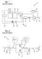
- FIG. 1 shows a known amplifier circuit 10. This includes a power supply with a supplied linear amplifier 12. At the output 14 of the linear amplifier 12, the amplified signal can be tapped. On one input side of the linear amplifier 12, the input signal supplied to an input 16 is supplied to it. The supply voltage is galvanically isolated from an input voltage resulting from the input signal. At the input signal In the example shown, this is a digital signal which is converted by means of a digital-to-analog converter 18 into an analog signal which can be processed by means of the linear amplifier 12. Of course, if the input signal is present as an analog signal, an input-side digital-to-analog conversion is not necessary.
- the gain by means of the linear amplifier 12 is designed as a controlled gain.
- the output signal is fed back by means of a return branch 20 to the input of the linear amplifier 12.
- the feedback takes place at a summation point 22 and with the inverse amplification factor of the linear amplifier 12.
- the return signal 20 is used to feed back the output signal supplied by 1 / G.
- the resulting controlled gain also causes gain to be increased by an intended gain.
- a DC-DC converter 24 (DC / DC converter) is provided.
- This comprises a first and a second switching stage 26, 28.
- the two switching stages 26, 28 are galvanically separated from each other, for example by way of an inductive coupling.
- the DC-DC converter 24 is supplied to its supply in the first switching stage 26, a supply voltage.
- the second switching stage 28 comprises an output filter, not shown here (for example, an output filter as in FIG FIG. 2 shown).
- an output signal of the DC-DC converter 24 is fed back by means of an amplifier 30 and via a galvanic isolation, for example in the form of an optocoupler 32, to the input of the DC-DC converter 24, namely an input-side pulse width modulator 34.
- the pulse width modulator 34 generates a pulse width modulated input signal for the first switching stage 26 of the DC-DC converter 24th
- a Class D amplifier 40 comprises a comparator 42, an amplifier stage 44 having two complementary switching elements in the form of transistors, MOSFETs or the like, and an output filter 46, here an RC element functioning as a low-pass filter.
- An analog signal is applied to an input 48 of the amplifier 40 as an input signal to be amplified, shown here in simplified form in the form of a sine signal.
- the amplifying input signal is converted into a pulse width modulated signal, as is also illustrated by the representation of the voltage applied to the output of the comparator 42 signal.
- the pulse width modulated signal is supplied to the amplifier stage 44, which causes the actual signal amplification.
- the advantage of the class D amplifier 40 is known to be that the switching elements are each either a maximum conductive or maximum insulating and thereby only very little power loss is generated.
- the amplified pulse width modulated signal at the output of the amplifier stage 44 is shown in FIG FIG. 2 shown symbolically and this is converted back into an analog signal by means of an output filter 46 terminating the circuit.
- the amplified output signal shown in the illustration for illustrative purposes is also shown as a sine signal with increased (amplified) amplitude can be tapped and this can be supplied to a speaker 52 or the like, for example.
- a class D amplifier 40 can be known as a DC-DC converter 24 (FIG. FIG. 1 ) be used.
- DC converter 24 FIG. 1
- FIG. 1 there is a concrete embodiment of the in FIG. 1 shown DC converter 24, for example, that act as the first switching stage 26, an amplifier stage 44 of a class D amplifier 40 and that act as the second switching stage 28, an output filter 46 of a class D amplifier 40.
- the disadvantage of the circuit in FIG. 1 is that the available power is limited by the losses of the linear amplifier 12. Especially with an output-side short circuit, high losses result and the resulting short-circuit current is difficult to handle.
- a class-D amplifier 40 as the DC-DC converter 24, its magnitude relative to the total losses corresponding to the characteristics of a class D amplifier 40 is comparatively low.
- the DC-DC converter 24 whose losses are still added to the losses of the linear amplifier 12.
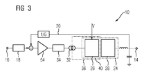
- an improved amplifier circuit 10 is accordingly proposed and disclosed in US Pat FIG. 3 an embodiment of such an amplifier circuit 10 is shown.
- the amplifier circuit 10 has an input 16 and an output 14.
- the amplifier circuit 10 can be supplied with the respective input signal to be amplified and is supplied to the same during operation.
- the amplified signal can be tapped off and is tapped there during operation of the amplifier circuit 10.
- the input signal is a digital signal, which by means of a digital-to-analog converter 18 on an input side of the amplifier circuit 10 in a first Analog signal is converted. Following the digital-to-analog converter 18 is a summation point.
- the feedback signal fed back by means of the return branch 20 and supplied with the inverse overall gain of the amplifier circuit 10 is coupled in. The feedback of the output signal leads to a total achieved with the amplifier circuit 10 regulated gain.
- the feedback output is subtracted from the input so that the resulting signal after the summation corresponds to an error remaining in the gain.
- the recirculated output signal is in the usual manner due to the feedback with a phase shift of 180 ° afflicted. An additional phase shift of 180 ° results due to the LC combination of the output filter 46.
- the total resulting phase shift is corrected by means of a phase shifter 54.
- a pulse width modulator 34 a pulse width modulation and the resulting pulse width modulated signal is applied via a galvanic isolation, for example in the form of an optocoupler 32, to the input of the DC voltage converter 24.
- This is a class D amplifier 40 ( FIG. 2 ) acting DC-DC converter 24 (DC / DC converter), so that its first switching stage 26 of the amplifier stage 44 of the class D amplifier 40 and the second switching stage 28 of the output filter 46 of the class-D amplifier 40th
- An advantage of the amplifier circuit 10 according to FIG. 3 is that by the gain by means of the class D amplifier 40 only very little power loss is generated. The previously with the within the amplifier circuit 10 ( FIG. 1 ) associated with power loss is thus avoided and the overall efficiency of the amplifier circuit 10 corresponds to the efficiency of the class D amplifier 40. Specifically falls in a provided by a battery or the like supply voltage V. particularly positive that the losses in the low power range are significantly reduced. The life of such a voltage source, in particular a battery, is significantly increased in this way. Another advantage is the reduction of the overall circuit complexity. This reduction is possible due to a "multiple use" of individual circuit parts, namely the pulse width modulator 34, the first and second switching stage 26, 28 and the output filter 46 of the DC / DC converter. These circuit parts are used at the same time for generating the supply voltage as for amplifying the input signal.
- the class-D amplifier 40 is supplied with the respective input-side supply voltage V.
- the galvanic isolation of the amplifier circuit 10 from the supply voltage V is achieved by the first switching stage 26 of the class D amplifier 40 on the input side and the output side of the rest of the amplifier circuit 10 is electrically isolated. On the input side, this can be done by means of an optocoupler 32 or by means of an inductive coupling. On the output side, the galvanic isolation in the form of an inductive coupling of the first switching stage 26 to the second switching stage 28 is realized.
- FIG. 4 shows a specific embodiment of the amplifier circuit 10 according to FIG. 3
- the peculiarity consists in a special embodiment of the class D amplifier 40.
- the input side digital-to-analog conversion and the feedback branch 20 for obtaining a controlled gain are identical to the amplifier circuit 10 according to FIG. 3
- the phase shifter 54 and the pulse width modulator 34 are identical.
- the pulse width modulator 34 is shown here with further details.
- a pulse width modulated form of an input signal can be achieved by means of a comparator 42, which receives the input signal at its one input and a triangular signal at its other input (see also FIG FIG. 2 ). This is in the illustration in FIG. 4 shown.
- the triangular signal supplied to the comparator 42 is produced on the basis of a square-wave signal by a frequency generator designated below as a clock generator 56.
- the first switching stage of the class D amplifier 40 is designed in the form of a bridge circuit with two oppositely driven bridges 60, 62.
- Each bridge 60, 62 includes two inductors 60A, 60B; 62A, 62B, each with opposite winding sense.
- Inductors 60A, 60B; 62A, 62B are used for input-side galvanic decoupling of the first switching stage 26.
- two drive signals (SW_A, SW_B) are generated for driving the first switching stage 26 by means of a phase compensation circuit 58 from the output signal of the pulse width modulator 34 and to each a respective bridge 60, 62 of the first switching stage 26 associated inductance 60A or 60B or 62A or 62B out.
- the control signals (SW_A, SW_B) are pulse width modulated signals.
- the bridge 60, 62 of the first switching stage 26 can therefore be controlled by means of pulse-width-modulated signals and by means of phase-shifted signals generated from pulse-width-modulated signals.
- the two bridges 60, 62 in the first switching stage 26 lead to an averaging-free energy transfer within the class D amplifier 40.
- a mean-free energy transfer is necessary to transfer the energy by means of a high-frequency transformer with a switching frequency of, for example, ten times to twenty times the highest frequency of the input signal.
- the drive signal (SW_A) guided to the first inductance 66 is generated for half the period of a pulse-width-modulated signal and the drive signal (SW_B) guided to the second inductance 68 is generated for the remainder of the period.
- the two bridges 60, 62 of the first switching stage 26 connect the two terminals of the transformer winding 70 alternately either with the supply voltage V or ground potential.
- the two terminal contacts are referred to differentiation according to the representation as the upper and lower terminal contact.
- the bridge 60 connects the upper terminal contact of the transformer winding 70 depending on the status of the drive signal SW_A either with the supply voltage V or ground potential and the bridge 62 connects the lower terminal contact depending on the status of the drive signal SW_B either ground potential or the supply voltage V.
- a vanishing voltage across The transformer winding 70 can be generated for example by both bridges 60, 62 - connect the transformer winding 70 on both sides with the supply voltage V or ground potential due to a control by means of corresponding control signals (SW_A, SW_B).
- the inductive coupling of the inductor 66 with one of the inductors 60A, 60B or - depending on the drive signal (SW_A, SW_B) - the inductive coupling of the inductor 68 with one of the inductors 62A, 62B forms a transformer on an input side of the first switching stage 26.
- Die inductive coupling of the transformer winding 70 and one of the middle tap outgoing halves of the transformer winding 72 forms a transformer on an output side of the first switching stage 26.
- the gain results from the generation of a pulse width modulated signal with the amplitude of the applied supply voltage V. Variations in the supply voltage V are with the balanced over the return branch 20 closed loop.
- a pulse-width-modulated signal resulting from the input signal on the input side of the first switching stage 26 with an amplitude of, for example 3V and a supply voltage V of 30V results in a gain by a factor of ten.
- the alternating coupling of the signal to be amplified into the first switching stage 26 is resolved again by means of an alternating output (synchronous rectification). This is done by means of the second switching stage 28.
- the local transformer winding 72 with the center tap is connected on both sides in each case to a switching element 74, 76.
- the transformer winding 72 is connected to the relevant side to ground potential.
- a section of the transformer winding 72 is coupled to the transformer winding 70 of the first switching stage 72 in the same direction or opposite sense winding.
- the control of the two switching elements 74, 76 by means of a controlled by the clock generator 56 switch 78.
- the switch 78 has two outputs, one of the outputs is an inverting output. Due to the resulting antivalent output signals of the switch 78, accordingly, exactly one of the two switching elements 74, 76 is always activated (switched on, conductive) and the other deactivated (open).
- the control signals (SW_A, SW_B) result from the phase-modulated input signal of the first switching stage 26. This in turn depends on the clock signal of the clock generator (timer) 56. From the clock signal of the clock generator 56 but also the control signals generated by means of the switch 78 for the switching elements 74, 76 are dependent.
- the galvanically isolated coupling into the first switching stage 26 and the coupling out of the first switching stage 26 thus take place on the same time base, namely on the basis of the clock signal generated by the clock generator 56. This ensures the in-phase extraction of the amplified signal.
- An amplifier circuit 10 and a method for its operation are disclosed, wherein the amplifier circuit 10 comprises a double-sided galvanically isolated and acting as an amplifier DC-DC converter 24, wherein an output signal of the amplifier circuit 10 is returned by means of a return branch 20 to an input-side summation point 22 and the DC-DC converter 24 is connected between the summation point 22 and an output-side output filter 46.
- the redundant in a separate structure of the power supply and the amplifying part circuit parts, namely the pulse width modulator 34, the first and second switching stage 26, 28 and the output filter 46 of the DC / DC converter, are used simultaneously to generate the supply voltage as to amplify the input signal ,
Landscapes
- Engineering & Computer Science (AREA)
- Power Engineering (AREA)
- Amplifiers (AREA)
Priority Applications (1)
| Application Number | Priority Date | Filing Date | Title |
|---|---|---|---|
| EP15170028.3A EP3101807A1 (fr) | 2015-06-01 | 2015-06-01 | Circuit d'amplification et procédé destiné au fonctionnement d'un circuit d'amplification |
Applications Claiming Priority (1)
| Application Number | Priority Date | Filing Date | Title |
|---|---|---|---|
| EP15170028.3A EP3101807A1 (fr) | 2015-06-01 | 2015-06-01 | Circuit d'amplification et procédé destiné au fonctionnement d'un circuit d'amplification |
Publications (1)
| Publication Number | Publication Date |
|---|---|
| EP3101807A1 true EP3101807A1 (fr) | 2016-12-07 |
Family
ID=53365817
Family Applications (1)
| Application Number | Title | Priority Date | Filing Date |
|---|---|---|---|
| EP15170028.3A Withdrawn EP3101807A1 (fr) | 2015-06-01 | 2015-06-01 | Circuit d'amplification et procédé destiné au fonctionnement d'un circuit d'amplification |
Country Status (1)
| Country | Link |
|---|---|
| EP (1) | EP3101807A1 (fr) |
Cited By (2)
| Publication number | Priority date | Publication date | Assignee | Title |
|---|---|---|---|---|
| DE102018119464A1 (de) * | 2018-08-09 | 2020-02-13 | Kögel, Willinger & Hell GbR (vertretungsberechtigter Gesellschafter: Reinhard Kögl, 78086 Brigachtal) | Schaltnetzteil sowie ein Verfahren zum Betreiben des Schaltnetzteils als Verstärker |
| US20210013848A1 (en) * | 2016-11-14 | 2021-01-14 | Siemens Schweiz Ag | Amplifier Circuit and Method for Operating an Amplifier Circuit |
Citations (4)
| Publication number | Priority date | Publication date | Assignee | Title |
|---|---|---|---|---|
| EP1269624B1 (fr) * | 2000-03-14 | 2006-09-13 | Harman International Industries, Incorporated | Systeme et procede de production de signaux audio directs a partir d'une source d'alimentation |
| WO2007049898A1 (fr) * | 2005-10-24 | 2007-05-03 | Samsung Electronics Co., Ltd. | Amplificateur audio numerique et procede d'amplification audio numerique associe |
| US20130121039A1 (en) * | 2011-11-15 | 2013-05-16 | Wen-Hsiung Hsieh | Switching amplifier with pulsed current supply |
| EP2667500A1 (fr) * | 2012-05-22 | 2013-11-27 | Siemens Aktiengesellschaft | Circuit d'amplification et procédé destiné au fonctionnement dýun circuit d'amplification |
-
2015
- 2015-06-01 EP EP15170028.3A patent/EP3101807A1/fr not_active Withdrawn
Patent Citations (4)
| Publication number | Priority date | Publication date | Assignee | Title |
|---|---|---|---|---|
| EP1269624B1 (fr) * | 2000-03-14 | 2006-09-13 | Harman International Industries, Incorporated | Systeme et procede de production de signaux audio directs a partir d'une source d'alimentation |
| WO2007049898A1 (fr) * | 2005-10-24 | 2007-05-03 | Samsung Electronics Co., Ltd. | Amplificateur audio numerique et procede d'amplification audio numerique associe |
| US20130121039A1 (en) * | 2011-11-15 | 2013-05-16 | Wen-Hsiung Hsieh | Switching amplifier with pulsed current supply |
| EP2667500A1 (fr) * | 2012-05-22 | 2013-11-27 | Siemens Aktiengesellschaft | Circuit d'amplification et procédé destiné au fonctionnement dýun circuit d'amplification |
Cited By (4)
| Publication number | Priority date | Publication date | Assignee | Title |
|---|---|---|---|---|
| US20210013848A1 (en) * | 2016-11-14 | 2021-01-14 | Siemens Schweiz Ag | Amplifier Circuit and Method for Operating an Amplifier Circuit |
| DE202017007564U1 (de) | 2016-11-14 | 2022-09-21 | Siemens Schweiz Ag | Verstärkerschaltung |
| US11552603B2 (en) * | 2016-11-14 | 2023-01-10 | Siemens Schweiz Ag | Amplifier circuit and method for operating an amplifier circuit |
| DE102018119464A1 (de) * | 2018-08-09 | 2020-02-13 | Kögel, Willinger & Hell GbR (vertretungsberechtigter Gesellschafter: Reinhard Kögl, 78086 Brigachtal) | Schaltnetzteil sowie ein Verfahren zum Betreiben des Schaltnetzteils als Verstärker |
Similar Documents
| Publication | Publication Date | Title |
|---|---|---|
| DE112008000106B4 (de) | Hochfrequenzleistungsversorgungsanordnung, insbesondere eine Plasmaversorgungseinrichtung und Verfahren zum Betreiben einer Hochfrequenzleistungsversorgungsanordnung | |
| DE69129340T2 (de) | Leistungsverstärker mit verschiedenen geschalteten Stufen | |
| DE69607013T2 (de) | Leistungswandler mit in beiden richtungen fliessendem strom | |
| DE69920099T2 (de) | Direktes Audiosignal aus der Speisespannung | |
| DE102011118581A1 (de) | Kontaktloses Energieübertragungssystem und Steuerverfahren dafür | |
| DE102008034109A1 (de) | Schaltung zur Nachbildung einer elektrischen Last | |
| DE2917926A1 (de) | Gegentakt-schaltleistungsverstaerker | |
| EP3134952A1 (fr) | Système de transmission et procédé de charge par induction d'un véhicule à propulsion électrique, et ensemble véhicule | |
| EP2709257A2 (fr) | Circuit de convertisseur de courant et procédé de commande du circuit de convertisseur de courant | |
| DE842502C (de) | Anordnung zur Verstaerkung eines breiten Frequenzbandes mittels im Gegentakt geschalteter, mit aussteuerungsabhaengigem Anodenstrom betriebener Roehren | |
| EP0025234B1 (fr) | Amplificateur de puissance basse fréquence et application à un émetteur à modulation d'amplitude | |
| EP2586646A2 (fr) | Dispositif électrique d'alimentation en énergie pour dispositifs d'entraînement destiné au fonctionnement d'un véhicule sur rail sur des réseaux d'alimentation électriques | |
| WO2011047818A1 (fr) | Dispositif de commande d'une pluralité de consommateurs électriques | |
| EP2449664B1 (fr) | Convertisseur continu-continu avec convertisseur auxiliaire destiné à compenser le courant de fuite | |
| WO2020048850A1 (fr) | Filtre actif à multiples chemins d'amplification | |
| DE202017007564U1 (de) | Verstärkerschaltung | |
| DE102013102433A1 (de) | Wechselrichter für eine variable Eingangsgleichspannung | |
| EP3101807A1 (fr) | Circuit d'amplification et procédé destiné au fonctionnement d'un circuit d'amplification | |
| DE102014200964A1 (de) | Verstärkeranordnung mit Tiefpassfiltereinrichtung | |
| DE2819676A1 (de) | Schalt-netzteil fuer hohe eingangsspannungen | |
| DE102014111451A1 (de) | System zur Anhebung des netzseitigen Leistungsfaktors von dreiphasig gespeisten EC-Motoren | |
| EP3360241B1 (fr) | Convertisseur continu-continu et procédé de fonctionnement d'un convertisseur continu-continu | |
| DE2953289C2 (fr) | ||
| EP2760103A1 (fr) | Symétrie de tensions de condensateurs dans une commutation en série de condensateurs | |
| DE19929841C2 (de) | Getakteter Verstärker, insbesondere zur Verstärkung von Audiosignalen |
Legal Events
| Date | Code | Title | Description |
|---|---|---|---|
| PUAI | Public reference made under article 153(3) epc to a published international application that has entered the european phase |
Free format text: ORIGINAL CODE: 0009012 |
|
| STAA | Information on the status of an ep patent application or granted ep patent |
Free format text: STATUS: THE APPLICATION HAS BEEN PUBLISHED |
|
| AK | Designated contracting states |
Kind code of ref document: A1 Designated state(s): AL AT BE BG CH CY CZ DE DK EE ES FI FR GB GR HR HU IE IS IT LI LT LU LV MC MK MT NL NO PL PT RO RS SE SI SK SM TR |
|
| AX | Request for extension of the european patent |
Extension state: BA ME |
|
| STAA | Information on the status of an ep patent application or granted ep patent |
Free format text: STATUS: REQUEST FOR EXAMINATION WAS MADE |
|
| STAA | Information on the status of an ep patent application or granted ep patent |
Free format text: STATUS: EXAMINATION IS IN PROGRESS |
|
| 17P | Request for examination filed |
Effective date: 20170519 |
|
| RBV | Designated contracting states (corrected) |
Designated state(s): AL AT BE BG CH CY CZ DE DK EE ES FI FR GB GR HR HU IE IS IT LI LT LU LV MC MK MT NL NO PL PT RO RS SE SI SK SM TR |
|
| 17Q | First examination report despatched |
Effective date: 20170619 |
|
| STAA | Information on the status of an ep patent application or granted ep patent |
Free format text: STATUS: THE APPLICATION HAS BEEN WITHDRAWN |
|
| 18W | Application withdrawn |
Effective date: 20170810 |