EP3101810A1 - Vorrichtung zur ansteuerung von igbt - Google Patents
Vorrichtung zur ansteuerung von igbt Download PDFInfo
- Publication number
- EP3101810A1 EP3101810A1 EP16170649.4A EP16170649A EP3101810A1 EP 3101810 A1 EP3101810 A1 EP 3101810A1 EP 16170649 A EP16170649 A EP 16170649A EP 3101810 A1 EP3101810 A1 EP 3101810A1
- Authority
- EP
- European Patent Office
- Prior art keywords
- igbt
- signal
- gate
- external capacitor
- power supply
- Prior art date
- Legal status (The legal status is an assumption and is not a legal conclusion. Google has not performed a legal analysis and makes no representation as to the accuracy of the status listed.)
- Withdrawn
Links
- 239000003990 capacitor Substances 0.000 claims abstract description 47
- 230000003071 parasitic effect Effects 0.000 description 16
- 238000007599 discharging Methods 0.000 description 8
- 230000009977 dual effect Effects 0.000 description 3
- 230000000694 effects Effects 0.000 description 3
- 238000010276 construction Methods 0.000 description 2
- 238000009434 installation Methods 0.000 description 2
- 230000007257 malfunction Effects 0.000 description 2
- 230000004048 modification Effects 0.000 description 2
- 238000012986 modification Methods 0.000 description 2
- 238000000034 method Methods 0.000 description 1
- 230000000630 rising effect Effects 0.000 description 1
- 239000004065 semiconductor Substances 0.000 description 1
- 238000006467 substitution reaction Methods 0.000 description 1
Images

Classifications
-
- H—ELECTRICITY
- H03—ELECTRONIC CIRCUITRY
- H03K—PULSE TECHNIQUE
- H03K17/00—Electronic switching or gating, i.e. not by contact-making and –breaking
- H03K17/51—Electronic switching or gating, i.e. not by contact-making and –breaking characterised by the components used
- H03K17/56—Electronic switching or gating, i.e. not by contact-making and –breaking characterised by the components used by the use, as active elements, of semiconductor devices
- H03K17/567—Circuits characterised by the use of more than one type of semiconductor device, e.g. BIMOS, composite devices such as IGBT
-
- H—ELECTRICITY
- H02—GENERATION; CONVERSION OR DISTRIBUTION OF ELECTRIC POWER
- H02M—APPARATUS FOR CONVERSION BETWEEN AC AND AC, BETWEEN AC AND DC, OR BETWEEN DC AND DC, AND FOR USE WITH MAINS OR SIMILAR POWER SUPPLY SYSTEMS; CONVERSION OF DC OR AC INPUT POWER INTO SURGE OUTPUT POWER; CONTROL OR REGULATION THEREOF
- H02M1/00—Details of apparatus for conversion
- H02M1/08—Circuits specially adapted for the generation of control voltages for semiconductor devices incorporated in static converters
-
- H—ELECTRICITY
- H03—ELECTRONIC CIRCUITRY
- H03K—PULSE TECHNIQUE
- H03K17/00—Electronic switching or gating, i.e. not by contact-making and –breaking
- H03K17/16—Modifications for eliminating interference voltages or currents
- H03K17/168—Modifications for eliminating interference voltages or currents in composite switches
-
- H—ELECTRICITY
- H03—ELECTRONIC CIRCUITRY
- H03K—PULSE TECHNIQUE
- H03K19/00—Logic circuits, i.e. having at least two inputs acting on one output; Inverting circuits
- H03K19/20—Logic circuits, i.e. having at least two inputs acting on one output; Inverting circuits characterised by logic function, e.g. AND, OR, NOR, NOT circuits
-
- H—ELECTRICITY
- H03—ELECTRONIC CIRCUITRY
- H03K—PULSE TECHNIQUE
- H03K5/00—Manipulating of pulses not covered by one of the other main groups of this subclass
- H03K5/01—Shaping pulses
- H03K5/08—Shaping pulses by limiting; by thresholding; by slicing, i.e. combined limiting and thresholding
-
- H—ELECTRICITY
- H03—ELECTRONIC CIRCUITRY
- H03K—PULSE TECHNIQUE
- H03K17/00—Electronic switching or gating, i.e. not by contact-making and –breaking
- H03K17/04—Modifications for accelerating switching
- H03K17/0406—Modifications for accelerating switching in composite switches
-
- H—ELECTRICITY
- H03—ELECTRONIC CIRCUITRY
- H03K—PULSE TECHNIQUE
- H03K17/00—Electronic switching or gating, i.e. not by contact-making and –breaking
- H03K17/06—Modifications for ensuring a fully conducting state
- H03K2017/066—Maximizing the OFF-resistance instead of minimizing the ON-resistance
Definitions
- the present invention relates to an apparatus for driving an Insulated Gate Bipolar Transistor, IGBT, and more particularly, to an apparatus for driving a single power supply of a high power IGBT.
- an IGBT Insulated Gate Bipolar Transistor
- a voltage region of 300V or higher particularly in a high-efficiency high-speed power system.
- a dual power supply or single power supply is used to such IGBT.
- a dual power supply refers to a power supply which uses a positive (+) voltage as a turn-on voltage and a negative (-) voltage as a turn-off voltage to drive an IGBT element.
- the dual power supply has a merit in that it may not consider a parasitic turn-on voltage which is caused by Miller capacitance and stray inductance, whereas it has a demerit from the viewpoint of installation cost and space.
- a single power supply refers to a power supply which uses a positive (+) voltage as a turn-on voltage and a zero (0) voltage as a turn-off voltage.
- the single power supply has a merit from the viewpoint of installation cost and space since it requires the less number of elements used, whereas it has a demerit in that parasitic turning-on may be caused by Miller capacitance and stray inductance.
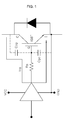
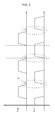
- Fig. 1 is an explanatory view showing a conventional IGBT single power supply driver and Fig. 2 is a graph used to explain a parasitic turn-on effect caused by the IGBT single power supply driver of Fig. 1 .
- a collector-emitter voltage Vce of IGBT rises, a current Icg is produced by collector-gate Miller capacitance.
- the collector-gate current Icg is converted into a voltage by a gate resistor Rg. As indicated by a dotted line in Fig. 2 , it can be seen that a parasitic voltage P due to the gate resistor Rg is generated at a rising edge of the collector-emitter voltage Vce.
- an apparatus for driving an IGBT including: a gate driver IC configured to supply a signal for driving the IGBT; an external capacitor connected between a gate and an emitter of the IGBT; a signal inverter configured to invert an output signal of the gate driver IC; and a switch configured to supply power to the external capacitor in response to an output signal of the signal inverter.
- the switch may open the external capacitor when the output signal of the gate driver IC has a high level, and may short-circuit the external capacitor when the output signal of the gate driver IC has a low level.
- the IGBT when the output signal of the gate driver IC has a high level, the IGBT may be turned on and the switch may be turned off.
- the IGBT when the output signal of the gate driver IC has a low level, the IGBT may be turned off, the switch may be turned on in response to an output signal having a high level supplied from the signal inverter, and the external capacitor may be charged with power supplied via the turned-on switch.
- the signal inverter may be composed of a NOT gate.
- the signal inverter is composed of a switching element for outputting an inverted signal.
- an IGBT single power supply driver which is capable of preventing a parasitic turn-on voltage from occurring without additional consumption, thereby allowing the driver to be operated with higher stability and efficiency.
- Fig. 3 is an explanatory view showing a typical Insulated Gate Bipolar Transistor, IGBT, single power supply driver.
- a typical IGBT single power supply driver is provided to overcome the problems described with reference to Figs. 1 and 2 and includes a gate driver IC for applying a control signal through an IGBT gate terminal.
- the gate driver IC has a clamp terminal 310 with an active Miller clamp function.
- an external capacitor (Cge_ext) 320 is interposed between the gate and the emitter of an IGBT.
- the active Miller clamp function refers to a function of reducing electrical vibration produced by Miller capacitance existing between the gate and the drain of the IGBT in an active way.
- the IGBT single power supply driver acts to be driven without malfunction due to the generation of the parasitic turn-on voltage.
- a circuit may be configured so as to maximize the capacitance of the external capacitor 320 through parallel connection of the capacitor.
- power Pg for driving only the IGBT element can be obtained according to the following equation 2.
- V is a driving voltage
- Qg is gate charge
- f c is a switching frequency.
- Pg V ⁇ Qg ⁇ f c
- the typical IGBT single power supply driver as shown in Fig. 3 requires additional power for charging/discharging of the gate-emitter 1 capacitor 320.
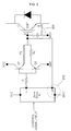
- Fig. 4 is an explanatory view showing an IGBT single power supply driver according to one embodiment of the present invention.
- an IGBT single power supply driver includes a signal inverter 430 connected to an output terminal of the gate driver IC and a switch 440 for switching power applied to the external capacitor 420 in correspondence to an output signal of the signal inverter 430, in addition to the typical IGBT single power supply driver as shown in Fig. 3 .
- the gate driver IC outputs a driving signal of the IGBT in correspondence to an input control signal.
- the driving signal output from the gate driver IC is input to a gate terminal of the IGBT element via switching elements Q1 and Q2 and gate resistors Rg.
- a current Icg is flown between the collector and the gate of the IGBT and is converted into a parasitic turn-on voltage via the gate resistors Rg, as described earlier.
- the IGBT single power supply driver as shown in Fig, 3 is suggested to overcome this problem.
- This IGBT single power supply driver prevents generation of the parasitic turn-on voltage through the charging/discharging of the external capacitor while discharging the current Icg via the clamp terminal of the gate driver IC.
- the IGBT single power supply driver acts to be driven without malfunction due to the generation of the parasitic turn-on voltage.
- the IGBT single power supply driver includes the signal inverter 430 such as a NOT gate or the like and the switch 440 such as a transistor, in addition to the above-described typical IGBT single power supply driver. More specifically, the IGBT single power supply driver according to one embodiment of the present invention includes the external capacitor 420 connected between the gate G and the emitter E of the IGBT, the signal inverter 430 for inverting the output signal of the gate driver IC, and the switch 440 for supplying power to the external capacitor 420based on the output signal of the signal inverter 430.
- the signal inverter 430 connected to the output terminal of the gate driver IC applies an inverted signal, which is obtained by inverting a signal applied to the IGBT, to the switch 440 through which power is then supplied to the external capacitor 420. Therefore, when the output signal of the gate driver IC has a high level, power for turning on the IGBT can be fully used as a driving signal of the IGBT. Conversely, when the output signal of the gate driver IC has a low level, a driving signal is used to charge the external capacitor 420 by means of the signal inverter 430, thereby preventing additional power consumption.
- the signal inverter 430 acts to output an Off signal to open the external capacitor 420 when the output signal of the gate driver IC has the high level and acts to output an On signal to short-circuit the external capacitor 420 when the output signal of the gate driver IC has the low level.
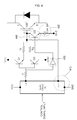
- Fig. 5 is an explanatory view showing an IGBT single power supply driver according to another embodiment of the present invention.
- an IGBT single power supply driver includes a signal inverter 435 which is composed of a switching element instead of the NOT gate in the IGBT single power supply driver shown in Fig. 4 .
- Fig. 5 shows a modification in which the signal inverter 435 is configured with a switching element instead of the NOT gate.
- the signal inverter 435 is implemented with a switching element such as a transistor and, when an output voltage of the gate driver IC is applied to a base terminal of the transistor, an output signal produced at a collector terminal of the transistor is used as an input signal of the switch 440.
- a switching element such as a transistor
- an output signal produced at a collector terminal of the transistor is used as an input signal of the switch 440.
- an inverted signal of the driving signal of the gate driver IC applied to the gate terminal of the IGBT is applied to the switch 440 via the signal inverter 435.
- the signal inverter 435 for generating an inverted signal of the output signal of the gate driver IC and supplying the inverted signal to the switch 440 may be implemented according to any schemes known in the art.
- the signal inverter 435 connected to the output terminal of the gate driver IC applies the inverted signal of the signal applied to the IGBT to the switch 440 and power is supplied to the external capacitor 420 via the switch 440. Therefore, when the output signal of the gate driver IC has a high level, power for turning on the IGBT can be fully used as a driving signal of the IGBT. Conversely, when the output signal of the gate driver IC has a low level, a driving signal is used to charge the external capacitor 420 by means of the signal inverter 435, thereby preventing additional power consumption, as described above with reference to Fig. 4 .
- the signal inverter 435 acts to output an Off signal to open the external capacitor 420 when the output signal of the gate driver IC has the high level and acts to output an On signal to short-circuit the external capacitor 420 when the output signal of the gate driver IC has the low level.
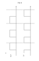
- Fig. 6 is a graph used to explain signal waveforms applied to an IGBT single power supply driver according to an embodiment of the present invention
- a signal Q3 for driving the switch 440 has the opposite waveform to the output signal OUT of the gate driver IC. This makes it possible to provide power for charging/discharging of the external capacitor without supply of additional power.
- Such an effect is shown to allow the IGBT single power supply driver to be operated with relatively little power while allowing the IGBT single power supply driver to be operated with higher stability and efficiency when the same power is used.
- the IGBT single power supply driver since the parasitic turn-on voltage is suppressed with increase in the capacitance of the external capacitor, even when an external capacitor with high capacitance is used or the external capacitor is implemented by parallel connection of a number of capacitors, the IGBT single power supply driver according to the embodiments of the present invention has an advantage that it can be operated with less power consumption than the typical IGBT single power supply driver.
- the IGBT single power supply driver includes a gate driver IC for outputting a control signal to drive an IGBT, an external capacitor connected between a gate and an emitter of the IGBT, a signal inverter for inverting an output signal of the gate driver IC, and a switch for supplying power to the external capacitor when the switch is turned on in response to the output signal of the signal inverter.
- the switch is turned on in response to an inverted signal of a signal output from the gate driver IC and is accordingly driven in the opposite way to the IGBT. That is, when the IGBT is turned off, the output signal of the gate driver IC is inverted by the signal inverter to turn on the switch and is supplied as power to the external capacitor.
- an IGBT single power supply driver which is capable of preventing a parasitic turn-on voltage due to an external capacitor and eliminating additional power form the external capacitor, thereby allowing the driver to be applied with higher stability and efficiency.
Landscapes
- Physics & Mathematics (AREA)
- Engineering & Computer Science (AREA)
- Computer Hardware Design (AREA)
- Computing Systems (AREA)
- General Engineering & Computer Science (AREA)
- Mathematical Physics (AREA)
- Nonlinear Science (AREA)
- Power Engineering (AREA)
- Power Conversion In General (AREA)
- Electronic Switches (AREA)
Applications Claiming Priority (1)
| Application Number | Priority Date | Filing Date | Title |
|---|---|---|---|
| KR1020150079102A KR20160143909A (ko) | 2015-06-04 | 2015-06-04 | Igbt 구동 장치 |
Publications (1)
| Publication Number | Publication Date |
|---|---|
| EP3101810A1 true EP3101810A1 (de) | 2016-12-07 |
Family
ID=56026767
Family Applications (1)
| Application Number | Title | Priority Date | Filing Date |
|---|---|---|---|
| EP16170649.4A Withdrawn EP3101810A1 (de) | 2015-06-04 | 2016-05-20 | Vorrichtung zur ansteuerung von igbt |
Country Status (5)
| Country | Link |
|---|---|
| US (1) | US20160359480A1 (de) |
| EP (1) | EP3101810A1 (de) |
| JP (1) | JP2017005698A (de) |
| KR (1) | KR20160143909A (de) |
| CN (1) | CN106253640A (de) |
Families Citing this family (11)
| Publication number | Priority date | Publication date | Assignee | Title |
|---|---|---|---|---|
| JP7157046B2 (ja) * | 2017-04-05 | 2022-10-19 | ローム株式会社 | パワーモジュール |
| JP7312561B2 (ja) * | 2018-02-25 | 2023-07-21 | 新電元工業株式会社 | パワーモジュール、スイッチング電源及びパワーコントロールユニット |
| JP2019201349A (ja) * | 2018-05-17 | 2019-11-21 | 矢崎総業株式会社 | スイッチング回路 |
| JP7140015B2 (ja) * | 2019-03-18 | 2022-09-21 | 株式会社デンソー | スイッチの駆動回路 |
| US11057029B2 (en) | 2019-11-25 | 2021-07-06 | Silicon Laboratories Inc. | Gate driver with integrated miller clamp |
| US10917081B1 (en) * | 2020-03-11 | 2021-02-09 | Silicon Laboratories Inc. | Adjustable soft shutdown and current booster for gate driver |
| US11362646B1 (en) | 2020-12-04 | 2022-06-14 | Skyworks Solutions, Inc. | Variable current drive for isolated gate drivers |
| US12155332B2 (en) | 2020-12-06 | 2024-11-26 | Skyworks Solutions, Inc. | Updating control parameters of a gate driver during operation |
| US11641197B2 (en) | 2021-04-28 | 2023-05-02 | Skyworks Solutions, Inc. | Gate driver output protection circuit |
| CN113472184B (zh) * | 2021-06-10 | 2023-12-15 | 矽力杰半导体技术(杭州)有限公司 | 驱动方法以及驱动电路 |
| CN118077128A (zh) * | 2021-10-13 | 2024-05-24 | 三菱电机株式会社 | 电力用半导体元件的驱动电路、电力用半导体模块以及电力变换装置 |
Citations (5)
| Publication number | Priority date | Publication date | Assignee | Title |
|---|---|---|---|---|
| JP2000333441A (ja) * | 1999-05-24 | 2000-11-30 | Toshiba Corp | 絶縁ゲート型半導体素子のゲート制御回路 |
| US20030075748A1 (en) * | 2001-10-19 | 2003-04-24 | Mitsubishi Denki Kabushiki Kaisha | Semiconductor device and method of driving transistors |
| US20040041201A1 (en) * | 2002-06-03 | 2004-03-04 | Kabushiki Kaisha Toshiba | Semiconductor device and capacitance regulation circuit |
| US20090058499A1 (en) * | 2007-08-27 | 2009-03-05 | Fuji Electric Device Technology Co., Ltd. | Gate driving circuit and method for driving semiconductor device |
| US7898303B2 (en) * | 2008-10-30 | 2011-03-01 | Infineon Technologies Austria Ag | Boost mechanism using driver current adjustment for switching phase improvement |
Family Cites Families (2)
| Publication number | Priority date | Publication date | Assignee | Title |
|---|---|---|---|---|
| JP4157010B2 (ja) * | 2003-10-27 | 2008-09-24 | 三菱電機株式会社 | 駆動回路及び半導体装置 |
| EP2216905B1 (de) * | 2009-02-05 | 2012-08-29 | Abb Oy | Verfahren zur Steuerung eines IGBT und eines Gate-Treibers |
-
2015
- 2015-06-04 KR KR1020150079102A patent/KR20160143909A/ko not_active Withdrawn
-
2016
- 2016-05-20 EP EP16170649.4A patent/EP3101810A1/de not_active Withdrawn
- 2016-06-02 JP JP2016110815A patent/JP2017005698A/ja active Pending
- 2016-06-02 US US15/172,003 patent/US20160359480A1/en not_active Abandoned
- 2016-06-03 CN CN201610391083.0A patent/CN106253640A/zh active Pending
Patent Citations (5)
| Publication number | Priority date | Publication date | Assignee | Title |
|---|---|---|---|---|
| JP2000333441A (ja) * | 1999-05-24 | 2000-11-30 | Toshiba Corp | 絶縁ゲート型半導体素子のゲート制御回路 |
| US20030075748A1 (en) * | 2001-10-19 | 2003-04-24 | Mitsubishi Denki Kabushiki Kaisha | Semiconductor device and method of driving transistors |
| US20040041201A1 (en) * | 2002-06-03 | 2004-03-04 | Kabushiki Kaisha Toshiba | Semiconductor device and capacitance regulation circuit |
| US20090058499A1 (en) * | 2007-08-27 | 2009-03-05 | Fuji Electric Device Technology Co., Ltd. | Gate driving circuit and method for driving semiconductor device |
| US7898303B2 (en) * | 2008-10-30 | 2011-03-01 | Infineon Technologies Austria Ag | Boost mechanism using driver current adjustment for switching phase improvement |
Also Published As
| Publication number | Publication date |
|---|---|
| KR20160143909A (ko) | 2016-12-15 |
| US20160359480A1 (en) | 2016-12-08 |
| CN106253640A (zh) | 2016-12-21 |
| JP2017005698A (ja) | 2017-01-05 |
Similar Documents
| Publication | Publication Date | Title |
|---|---|---|
| US20160359480A1 (en) | Apparatus for driving insulated gate bipolar transistor | |
| JP3666843B2 (ja) | 絶縁ゲート型半導体素子のゲート回路 | |
| US9461640B2 (en) | Switching element drive circuit, power module, and automobile | |
| US9397658B2 (en) | Gate drive circuit and a method for controlling a power transistor | |
| EP2015453B1 (de) | Treiberschaltung für ein spannungsgesteuertes Schaltelement | |
| CN104866000B (zh) | 具有稳压器的栅极驱动电路及方法 | |
| JPH10248237A (ja) | 電力変換装置 | |
| WO2012153836A1 (ja) | スイッチング回路及び半導体モジュール | |
| JP5619673B2 (ja) | スイッチング回路及び半導体モジュール | |
| US8760200B2 (en) | Gate driving apparatus | |
| CN107395000B (zh) | 半导体器件 | |
| JP2023516357A (ja) | パワーデバイスの駆動回路及び駆動システム | |
| CN106464122A (zh) | 控制电子开关的集电极到发射极电压变化的栅极驱动器以及包括所述栅极驱动器的电路 | |
| US8638134B2 (en) | Gate drive circuit and power semiconductor module | |
| CN105706366A (zh) | 栅极驱动电路以及使用该栅极驱动电路的电力变换装置 | |
| JP2011182578A (ja) | 電力変換装置 | |
| JP2017079534A (ja) | ゲート制御回路 | |
| US8258823B2 (en) | Method of and driver circuit for operating a semiconductor power switch | |
| JP2014150654A (ja) | ゲート駆動回路 | |
| US6774682B2 (en) | Circuit configuration for driving a semiconductor switching element and method for same | |
| KR20040029082A (ko) | 하프 브리지 회로 및 이를 포함하는 장치 | |
| US6542012B2 (en) | Circuit for driving gate of IGBT inverter | |
| KR20110139886A (ko) | 인버터의 게이트 드라이브 회로 | |
| KR101841159B1 (ko) | 스위칭 게이트 드라이브 | |
| JP4321491B2 (ja) | 電圧駆動型半導体素子の駆動装置 |
Legal Events
| Date | Code | Title | Description |
|---|---|---|---|
| PUAI | Public reference made under article 153(3) epc to a published international application that has entered the european phase |
Free format text: ORIGINAL CODE: 0009012 |
|
| STAA | Information on the status of an ep patent application or granted ep patent |
Free format text: STATUS: THE APPLICATION HAS BEEN PUBLISHED |
|
| AK | Designated contracting states |
Kind code of ref document: A1 Designated state(s): AL AT BE BG CH CY CZ DE DK EE ES FI FR GB GR HR HU IE IS IT LI LT LU LV MC MK MT NL NO PL PT RO RS SE SI SK SM TR |
|
| AX | Request for extension of the european patent |
Extension state: BA ME |
|
| STAA | Information on the status of an ep patent application or granted ep patent |
Free format text: STATUS: REQUEST FOR EXAMINATION WAS MADE |
|
| 17P | Request for examination filed |
Effective date: 20170531 |
|
| RBV | Designated contracting states (corrected) |
Designated state(s): AL AT BE BG CH CY CZ DE DK EE ES FI FR GB GR HR HU IE IS IT LI LT LU LV MC MK MT NL NO PL PT RO RS SE SI SK SM TR |
|
| STAA | Information on the status of an ep patent application or granted ep patent |
Free format text: STATUS: EXAMINATION IS IN PROGRESS |
|
| 17Q | First examination report despatched |
Effective date: 20200414 |
|
| STAA | Information on the status of an ep patent application or granted ep patent |
Free format text: STATUS: THE APPLICATION HAS BEEN WITHDRAWN |
|
| 18W | Application withdrawn |
Effective date: 20200814 |