EP3104455B1 - Agencement de rayonnement dipolaire - Google Patents
Agencement de rayonnement dipolaire Download PDFInfo
- Publication number
- EP3104455B1 EP3104455B1 EP16172969.4A EP16172969A EP3104455B1 EP 3104455 B1 EP3104455 B1 EP 3104455B1 EP 16172969 A EP16172969 A EP 16172969A EP 3104455 B1 EP3104455 B1 EP 3104455B1
- Authority
- EP
- European Patent Office
- Prior art keywords
- radiator
- dipole
- line
- support
- halves
- Prior art date
- Legal status (The legal status is an assumption and is not a legal conclusion. Google has not performed a legal analysis and makes no representation as to the accuracy of the status listed.)
- Active
Links
Images



Classifications
-
- H—ELECTRICITY
- H01—ELECTRIC ELEMENTS
- H01Q—ANTENNAS, i.e. RADIO AERIALS
- H01Q9/00—Electrically-short antennas having dimensions not more than twice the operating wavelength and consisting of conductive active radiating elements
- H01Q9/04—Resonant antennas
- H01Q9/16—Resonant antennas with feed intermediate between the extremities of the antenna, e.g. centre-fed dipole
- H01Q9/28—Conical, cylindrical, cage, strip, gauze, or like elements having an extended radiating surface; Elements comprising two conical surfaces having collinear axes and adjacent apices and fed by two-conductor transmission lines
- H01Q9/285—Planar dipole
-
- H—ELECTRICITY
- H01—ELECTRIC ELEMENTS
- H01Q—ANTENNAS, i.e. RADIO AERIALS
- H01Q1/00—Details of, or arrangements associated with, antennas
- H01Q1/50—Structural association of antennas with earthing switches, lead-in devices or lightning protectors
-
- H—ELECTRICITY
- H01—ELECTRIC ELEMENTS
- H01Q—ANTENNAS, i.e. RADIO AERIALS
- H01Q1/00—Details of, or arrangements associated with, antennas
- H01Q1/12—Supports; Mounting means
- H01Q1/22—Supports; Mounting means by structural association with other equipment or articles
- H01Q1/24—Supports; Mounting means by structural association with other equipment or articles with receiving set
- H01Q1/241—Supports; Mounting means by structural association with other equipment or articles with receiving set used in mobile communications, e.g. GSM
- H01Q1/246—Supports; Mounting means by structural association with other equipment or articles with receiving set used in mobile communications, e.g. GSM specially adapted for base stations
-
- H—ELECTRICITY
- H01—ELECTRIC ELEMENTS
- H01Q—ANTENNAS, i.e. RADIO AERIALS
- H01Q1/00—Details of, or arrangements associated with, antennas
- H01Q1/36—Structural form of radiating elements, e.g. cone, spiral, umbrella; Particular materials used therewith
-
- H—ELECTRICITY
- H01—ELECTRIC ELEMENTS
- H01Q—ANTENNAS, i.e. RADIO AERIALS
- H01Q1/00—Details of, or arrangements associated with, antennas
- H01Q1/48—Earthing means; Earth screens; Counterpoises
-
- H—ELECTRICITY
- H01—ELECTRIC ELEMENTS
- H01Q—ANTENNAS, i.e. RADIO AERIALS
- H01Q19/00—Combinations of primary active antenna elements and units with secondary devices, e.g. with quasi-optical devices, for giving the antenna a desired directional characteristic
- H01Q19/10—Combinations of primary active antenna elements and units with secondary devices, e.g. with quasi-optical devices, for giving the antenna a desired directional characteristic using reflecting surfaces
- H01Q19/12—Combinations of primary active antenna elements and units with secondary devices, e.g. with quasi-optical devices, for giving the antenna a desired directional characteristic using reflecting surfaces wherein the surfaces are concave
-
- H—ELECTRICITY
- H01—ELECTRIC ELEMENTS
- H01Q—ANTENNAS, i.e. RADIO AERIALS
- H01Q21/00—Antenna arrays or systems
- H01Q21/24—Combinations of antenna units polarised in different directions for transmitting or receiving circularly and elliptically polarised waves or waves linearly polarised in any direction
-
- H—ELECTRICITY
- H01—ELECTRIC ELEMENTS
- H01Q—ANTENNAS, i.e. RADIO AERIALS
- H01Q9/00—Electrically-short antennas having dimensions not more than twice the operating wavelength and consisting of conductive active radiating elements
- H01Q9/04—Resonant antennas
- H01Q9/16—Resonant antennas with feed intermediate between the extremities of the antenna, e.g. centre-fed dipole
-
- H—ELECTRICITY
- H01—ELECTRIC ELEMENTS
- H01Q—ANTENNAS, i.e. RADIO AERIALS
- H01Q9/00—Electrically-short antennas having dimensions not more than twice the operating wavelength and consisting of conductive active radiating elements
- H01Q9/04—Resonant antennas
- H01Q9/16—Resonant antennas with feed intermediate between the extremities of the antenna, e.g. centre-fed dipole
- H01Q9/18—Vertical disposition of the antenna
-
- H—ELECTRICITY
- H01—ELECTRIC ELEMENTS
- H01Q—ANTENNAS, i.e. RADIO AERIALS
- H01Q9/00—Electrically-short antennas having dimensions not more than twice the operating wavelength and consisting of conductive active radiating elements
- H01Q9/04—Resonant antennas
- H01Q9/16—Resonant antennas with feed intermediate between the extremities of the antenna, e.g. centre-fed dipole
- H01Q9/28—Conical, cylindrical, cage, strip, gauze, or like elements having an extended radiating surface; Elements comprising two conical surfaces having collinear axes and adjacent apices and fed by two-conductor transmission lines
Definitions
- the invention relates to a dipole radiator arrangement according to claim 1.
- Dipole radiators are for example from the Vorveröttingungen DE 197 22 742 A such as DE 196 27 015 A known.
- Such dipole radiators can have a conventional dipole structure in the form of a simple dipole or consist for example of a crossed dipole or a dipole square, etc.
- a so-called vector dipole is eg from the pre-publication WO 00/39894 A1 known. Its structure seems to be comparable to a dipole square.
- due to the specific design of the dipole radiator according to this prior publication and the special feed of this dipole radiator acts much like a cross dipole, which radiates in two polarization planes perpendicular to each other. In constructive In particular, it is rather square because of its outer contour design.
- Such dipole radiators are usually fed in such a way that a dipole or radiator half is DC-connected (ie galvanically) to an outer conductor, whereas the inner conductor of a coaxial connecting cable is connected to the second dipole or radiator half in a DC manner (ie in turn galvanically).
- the feed takes place in each case at the mutually facing end portions of the dipole or radiator halves.
- the support means or the respectively associated half of the support means of the radiator arrangement can therefore also capacitively coupled to ground at its base or at its base to ground or galvanically connected to the reflector and thereby be grounded.
- such single- or dual-polarized emitters can also have a very broadband design so that they can transmit and / or receive in different frequency ranges or frequency bands.
- radiators can usually be superimposed in one or more antenna columns.
- Such antenna arrays can also be controlled, for example using phase shifters, in particular differential phase shifters, with different phase, so that a different down-angle can be set.
- phase shifters in particular differential phase shifters, with different phase, so that a different down-angle can be set.
- a possible arrangement using multiple-phase shifters for different setting of a down-tilt angle with corresponding supply of dual-polarized radiators is for example from EP 2 406 851 B1 refer to.
- the feed is usually asymmetrical using a coaxial cable, which thus comprises a cable structure with a signal line and a ground line.
- a single-polarized dipole radiator is usually fed by means of a coaxial cable, wherein the outer conductor of the coaxial cable is soldered at the inner end of one of the radiator halves approximately at the level of the radiator halves, ie in particular the dipole halves.
- the inner conductor is passed over it, to the adjacent inner end of the second radiator half, i. in the specific case of the second dipole half, where the inner conductor forming the signal line is soldered.
- a corresponding supply also takes place via a coaxial conductor for each of the two polarization planes, as explained above.
- a dipole-shaped radiator is further from the US 2003/0193377 A1 known.
- the publication describes a feed point at the dipole point. Via the network, a specific signal is generated at the feed station.
- the mentioned MEM switches are arranged. This makes it possible to realize a switching of the supply, which leads to a 180 ° phase shift. This is equivalent to a reversal of the current flow in the feed of the dipole.
- the object of the present invention is now to provide an improved feed structure on the basis of such a prior art.
- a significantly improved feed structure is created in a surprising manner, which is not only advantageous on its own, but also opens up a number of advantageous application possibilities.
- asymmetrical feed structure for example using a coaxial cable, for which at least one plane of polarization is fed twice.
- a double-feed can be realized for the preferably two polarization planes.
- a ground conductor is not only galvanically or optionally also capacitively coupled to the one radiator half and the associated signal conductor on the opposite radiator half, but that next to it a second feed structure is provided.
- This second radiator structure is basically the same or similar, but the ground conductor of the second feed structure preferably at the inner end of those Hallower half is galvanically or capacitively connected, to which the signal or inner conductor of the first feed structure is coupled. Conversely, the signal or inner conductor of the second feed structure is continued beyond the ground conductor to the second radiator half belonging to the same plane of polarization and there coupled galvanically or capacitively, ie with the radiator half, in which the ground conductor of the first feed structure is coupled.
- the ground connection to the radiator device can also take place in a region below the actual radiator halves or dipole halves. for example, at the level of the base of the support means of the radiator structure.
- This double feed allows, for example, that the same physical radiator for two different frequency ranges can be fed via different upstream phase shifters. This makes it possible in the simplest way to operate the same physical radiator, for example, in two different frequency bands and these frequency bands via upstream phase shifter different in their down-tilt range or to change this lowering angle.
- This improvement can be realized without additional increase in the required installation space on the reflector back of such a radiator arrangement or such a radiator array. Because today's generation of particular intended for mobile antennas is fitted on the back of the reflector usually provided with a variety of components, so that there is hardly any free space available.
- the inventively proposed feed structure requires only that from the back of the reflector, via corresponding passages or holes, the corresponding unbalanced lines to the radiator side of the reflector, ie to the so-called front or front side are passed, up to the corresponding coupling points where the signal lines and the ground lines are coupled to the respective radiator halves.
- the invention also opens up the possibility that the aforementioned asymmetrical radiator structure can be implemented in a simple manner not only using coaxial cables, but also using another, two-line feed system, for example in the form of a micro-strip line, a coplanar line arrangement , an arrangement using single or multilayer boards which are part of the dipole structure and which on the preferably opposite side to the electrically conductive surface of Carrying device of the radiator structure and / or the radiator or dipole structure itself are provided with the aforementioned micro-strip line, which is once designed as a ground line and once as a signal line.
- FIG. 1 is a schematic plan view of an antenna array, that is shown in the concrete, a single-column antenna array 1, which is usually mounted extending in the vertical direction.
- This antenna array 1 comprises a reflector 3, which in a vertical plan view in FIG FIG. 1 is shown.
- V of the antenna array 1 are generally mounted at equidistant intervals A radiator 5 (distance A between two neighboring in the V direction centers of two radiators).
- FIG. 1 For example, two single-polarized radiators 5a arranged at a distance from one another in the direction V are reproduced, whose two dipole radiator halves 7.1a and 7.1b are aligned transversely and in particular perpendicular to the vertical or longitudinal direction V.
- an associated, perpendicular to the reflector plane RE extending polarization plane P1 is defined, which in FIG. 1 is shown in dashed lines and perpendicular to the reflector plane RE and thus perpendicular to the plane.
- a dipole-shaped cross-radiator 5b is shown for clarity, and a so-called vector radiator 5c is again offset, having two polarization planes P1 and P2 oriented perpendicular to one another.
- An equally usable dipole square is not shown for clarity, but could be used as well.
- radiators 5a are simply polarized dipole radiators
- the in FIG. 1 represented Dipolnch 5b and the vector dipole 5c in two mutually perpendicular polarization planes P1 and P2 send and / or can receive, as well as, for example, in a correspondingly aligned dipole square.
- the actual radiator elements i. the dipole halves 7.1a and 7.1b with singly polarized radiators and the radiator halves 7.1a, 7.1b and 7.2a, 7.2b in dual polarized radiators usually extend at a distance from the reflector 3 in parallel alignment with the reflector plane RE.
- radiators are only examples in FIG. 1 to clarify that an antenna array 1 can be constructed using a variety of radiators 5a, 5b and / or 5c, ie using emitters of the same type or of radiators with different designs.
- the structures can thus be different, whereby differently shaped radiators can be used, which radiate in different bands.
- vector emitters 5c these can be designed in a very broadband fashion so that they can transmit and / or receive in at least two or even several mutually offset frequency bands.
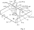
- FIG. 2 is a corresponding spatial representation of the in FIG. 1 shown antenna array, but only under a simplified view of a simple dipole radiator 5a, which radiates only in a polarization plane P1.
- Such dipole-shaped radiators usually have a carrier 11 which, in the case of a dipole radiator 2, comprises carrier halves 11.1a and 11.1b which extend from the reflector plane RE of the reflector 3 to the level of the dipole halves 7.1a and 13b extending laterally away from one another 7.1b, with the formation of a slit 13.1 provided therebetween, which in the case of a dipole can also be referred to as Symmetri mecanicsschlitz 13.1.
- the dipole halves 7.1a and 7.1b are separated from each other at the level of the radiators via the mentioned slot 13.1, and thus have adjacent to each other so-called inner Strahlerendabroughe 107, i. 107.1a and 107.1b and removes lying outwardly facing Strahlerendabête 117.1a and 117.1b, which are hereinafter also referred to as outer Strahlerendabchae 117.1a, 117.1b.
- Such a dipole or generally dipole radiator may be made of a conductive metal, such as a casting.
- a corresponding dipole for example a crossed dipole, may also consist of a sheet metal part or be made of a sheet metal part which can be shaped accordingly by tilting, punching, edging and / or bending.
- dipole radiators can also be made, for example, using a dielectric, e.g. be formed in the form of a single or multi-layer board or using a corresponding board material, which at least on one side, i. the front or the back is covered with a metallized layer. Preferably, the entire surface is metallized accordingly.
- the slot 13.1 extends, as mentioned, almost over the entire height of the dipole or may deviate in the illustrated embodiment FIG. 2 one below to the reflector 3 lying, the two carrier halves 11.1a and 11.1b connecting connecting web 15.1 have, whereby the entire common base 17 of the carrier 11.1 and thus the base 17 of the radiator 5 is formed.
- This connecting web 15.1 is one of the possible variants in FIG. 2 drawn only by dashed lines, since the radiator halves 7.1a and 7.1b can also extend to the reflector plane RE through the slot 13 separately.
- connection of the underside of the carrier 11.1 or the carrier halves 11.1a, 11.1b with or without additional connecting web 15.1 preferably be realized by means of a galvanic contacting with the conductive reflector 3 , but also possible here is the formation of a capacitive connection. If an insulating intermediate layer between the base 17, so the bottom of the base 17 (with or without in FIG. 2 shown connecting web 15.1) and the electrically conductive reflector layer is provided, thereby generating a capacitive coupling of the respective radiator on the reflector 3. In other words, a capacitive or, if necessary, a galvanic connection to the reflector can be provided here on the base 17 of the carrier 11.
- the feed height or the eating plane SpE is usually provided, which in FIG. 2 is shown in dashed form, this plane is parallel to the reflector plane RE.
- this feed height or feed level the feeding of the transmission signals or the received signals, which is explained in detail below, usually takes place.
- the feed can certainly be provided in a certain range even below the height range in which the dipole or radiator halves 7.1a, 7.1b are formed.
- the radiator height H with respect to the reflector plane RE and thus more or less the length of the slot 13.1 generally correspond to a value of about ⁇ / 4.
- the radiator height and / or the slot length should preferably not fall below a value of ⁇ / 10.
- the radiator height could basically be an arbitrary multiple of ⁇ (especially since a radiator has a radiation diagram even without a reflector).
- ⁇ preferably represents a wavelength from the frequency band to be transmitted, preferably in a middle frequency of the band to be transmitted. If it is a broadband radiator transmitting two or more frequency bands, the value of ⁇ should preferably be a mean size of the entire frequency band range from the lowest to the highest value of the different frequency bands.
- FIG. 3a is a schematic side view, in FIG. 3b in spatial view and in Figure 3c in plan view a section of the dipole radiator 7.1 according to FIG. 1 and 2 reproduced, namely with its two carrier halves 11.1a, 11.1b and the lower connecting web 15, without the running away at the upper end of the carrier 11.1 dipole or radiator halves 7.1a, 7.1b, the only in FIG. 3a are indicated.
- such a dipole radiator is fed asymmetrically, using a two-line feed 21.1, 21.1a, e.g. in the form of an asymmetrical coaxial cable 121.1a, which is guided from the underside or rear side of the reflector 3 via a recess or bore in the reflector 3 to the radiator side and then along a support half, for example, the carrier half 11.1a towards the top lying end of the carrier 11.1 out running is.
- a two-line feed 21.1, 21.1a e.g. in the form of an asymmetrical coaxial cable 121.1a, which is guided from the underside or rear side of the reflector 3 via a recess or bore in the reflector 3 to the radiator side and then along a support half, for example, the carrier half 11.1a towards the top lying end of the carrier 11.1 out running is.
- the upper end of the ground conductor 25.1 in the case of a coaxial cable 125a in the form of an outer conductor 125.1a, can be capacitively and preferably galvanically connected, in particular by soldering, to the electrically conductive surface of the adjacent carrier half 11a, ie, for example at a ground feeding point 126.1a.
- the outer conductor of the in FIGS. 3a to 3c shown coaxial cable 125.1 still surrounded by an insulating outer sheath, which leads to the vicinity of the feed point 126.1a, where the then exposed outer conductor is soldered to the upper end of the carrier of the radiator.
- This insulating outer sheath is not shown in the figures for the sake of simplicity.
- ⁇ represents, however, as a rule and preferably the mean wavelength of the frequency band to be transmitted.
- the signal line 27.1 extends, here in the form of an inner conductor 127.1a of the coaxial cable 121.1a, wherein the inner conductor is also passed over the slot 13 and capacitively or galvanically connected to the opposite portion of the other dipole or radiator half 7.1b.
- the connection should be done galvanically, for example by means of soldering.
- the signal coupling takes place via the signal line here in the form of the inner conductor 27.1a at a signal feed point 128.1b at the top and inner region of the second carrier half 11b.
- the supply carried out at there formed dining points or points 126.1a and 128.1b, by at the one dining place 126.1a of the ground conductor 25.1a and at the other feed point 126.1b of the signal conductor 27.1a is connected galvanically or capacitively.
- FIGS. 3a to 3c But how about the FIGS. 3a to 3c It can also be seen, in the context of the invention to the same radiator or dipole 5 still a second feed 21.1b is provided, which is formed exactly the opposite of the first.
- the second two-line feed 21.1b may be provided, for example in the form of another coaxial cable 121.1b, which, for example, on the second carrier half 11.1b from the back of the reflector via a bore in the outer or inner reflector in the upper direction End of the carrier 11.1 is designed to extend.
- the associated ground conductor 25.1b in the form of the associated outer conductor 125.1b is in turn capacitively or galvanically connected to the associated carrier 11.1b in the region of the overhead feed point 126.1b and thus capacitively or galvanically connected to the associated dipole or radiator half 7.1b
- the signal line 27.1b, here in the form of the inner conductor 127.1b over the slot 13 away in the reverse direction to the inner conductor 127.1a of the first two-line feed 21.1a to the opposite portion of the carrier half 11.1a and thus to the inner feed point 128.1a at the inner radiator end portion 107.1a of the associated dipole or radiator half 7.1a running trained and connected there galvanically or capacitively.
- the same radiator 5 can be operated, for example, in two different frequency ranges, wherein the one frequency band in the transmitting and / or receiving direction via the one two-line feed 21.1a, here in the form of coaxial cable 121.1a, and another Two-line feed 21.1b can be done for example for a second frequency range via the second coaxial cable 121.1b.
- the peculiarity is that the two coaxial cables 121.1a and 121.1b can be preceded by different phase adjustment devices, for example in the form of phase shifters and in particular differential phase shifters, so that the different frequency ranges that transmit and receive via the same radiators 5 are different and different from each other separate down-tilt angles can be easily adjusted.
- the coaxial cables 121.1a, 121.1b arranged with their ground or outer conductors and their inner or signal conductors on the same side of the associated dipole or radiator 5, for example on the in the FIGS. 3a and 3b Therefore, the two outer conductors 125.1a and 125.1b terminate in slightly different height H1 or H2 with respect to the reflector plane RE, ie the underside of the base 17.1, so that the lines can be mounted without collision.
- this is a coaxial two-line feed system 21.1a, for example formed on the first or front side 31 of the preferably perpendicular to the reflector plane RE rising Stahlers or dipole, whereas the second two-line feeder 21.1b is formed on the opposite second or rear side 32 of the dipole or radiator 5, ie in plan view of a about a leading through the center of the radiator and perpendicular to the reflector plane RE central axis rotated by 180 ° alignment and arrangement.
- the feed points 126.1a and 126.1b for the ground or outer conductors of the two coaxial cables 121.1a and 121.1b as well as the feed points 128.1b and 128.1a for the inner or signal conductors 27.1a, 27.1b are usually on same height level H1, although here, too, a certain height difference would be quite possible.
- this embodiment is a cross-shaped dipole radiator 5b which transmits and receives in two mutually perpendicular polarization planes P1 and P2.
- the further difference to the previous embodiment is that the unbalanced two-line system 21.1 and 21.1b is realized not by means of coaxial cable 121, but by using microstrip lines 221 (strip lines).
- the cross-shaped radiator 5b comprises two perpendicular dipoles 7.1 and 7.2, each with two in the associated plane of polarization P1, P2 dipole or radiator halves 7.1a, 7.1b and 7.2a, 7.2b, wherein the polarization planes P1 , P2, as in the first embodiment also, are aligned perpendicular to the reflector plane RE according to the design of the radiator.
- the two polarization planes P1 and P2 intersect at the center of the radiators such that the two dipole halves 7.1a, 7.1b lie in the first polarization plane P1 and the two perpendicular radiator or dipole halves 7.2a, 7.2b in the second polarization plane P2.
- Each of the carriers 11.1 and 11.2 lying parallel to the planes of polarization P1, P2 with the associated carrier halves 11.1a and 11.1b or 11.2a, 11.2b can be made of metal or metal plates, in particular of one or more assembled sheet metal parts. It is also possible that these carriers are formed, for example, from printed circuit board material, ie from a dielectric, wherein at least one and preferably both of the opposite side surfaces are coated with an electrically conductive layer, which are preferably galvanically connected to one another.
- the paired carrier halves 11.1a, 11.1b and 11.2a, 11.2b which are perpendicular to each other with respect to both polarization planes P1, P2, can be mounted and / or held on a common base 17, with which they are preferably also electrically connected , Via a provided for example in the middle of the base 17 bore 18 then the base as well as the radiator can be connected in total galvanic or capacitive as explained with an electrically conductive reflector, whereby it is electrically connected and mechanically held accordingly.
- the two feed systems are basically similar and similar to the previous embodiment.
- connection of a ground line 25 (as generally based on FIGS. 3a and 3b already described), ie in the present case, the connection of a ground line 25.1a, 25.1b or 25.2a, 25.2b, for example via the galvanic connection of the lower end of the carrier 11, ie the respective carrier halves 11.1a, 11.1b and 11.2a, 11.2b not only directly, but also for example via the electrically conductive base 17 with the reflector 3 and / or a separate mass Connection lead (which in the FIGS. 5a to 5e not shown).
- a galvanic or capacitive connection of the ground line for example in the vicinity of the upper portions of a carrier half 11.1a, 11.1b and 11.2a, 11.2b are performed, as based on FIGS. 3a to 4c explained.
- the in the embodiment according to FIGS. 5a to 5e respectively provided two signal lines 27.1a, 27.1b and 27.2a, 27.2b (of which, due to the illustration, only the signal lines located on one side of the carrier halves 27.1a and 27.2a are visible) are in this embodiment preferably each as a micro-strip -Leitung (ie as a strip line) 221.a, 221b and 221.2a, 221.2b formed, so as a conductor on a corresponding dielectric 128, for example in the form of a printed circuit board material 128, which thus serves as a substrate or support, here in specific as a support plate.
- a micro-strip -Leitung ie as a strip line
- the design of the respective ground line 25.1a, 25.1b and 25.2a, 25.2b in microstrip form 221.1a, 221.1b or 221.2a, 221.2b designed in a lateral plan view in the manner of an inverted L or approximately L-shaped designed, including the associated Carrier or the substrate 128 may be designed with appropriate shape but can not.
- This printed circuit board material 128 with the microstrip feed or signal line 27.1, 27.2 thereon is in each case in parallel contact with the actual plate-shaped carrier 11, for each polarization P1 or P2. the respective carrier half 11.1 or 11.2, for each polarization in the form of the carrier half 11.1a, 11.1b or 11.2a, 11.2b adjacent or provided at a small distance.
- the electrically conductive surface of the carrier 11 serves as a ground plane for the spaced apart by the thickness of the substrate 128 to the micro-strip conductor track.
- the signal lines 27.1a, 27.1b and 27.2a, 27.2b are preferably respectively facing outward on the associated non-conductive surface of the carrier 11.
- an associated ground surface may be formed on the immediate, opposite rear side of the substrate 128 for forming the microstrip interconnects, which is preferably separated from the ground plane of the carrier halves with the interposition of a dielectric film or with the interposition of an air gap.
- the structure is, for example, for the polarization P1 such that the corresponding in the form of an inverted L approximate support structure is positioned in the form of the carrier 128 with the conductor thereon 127.1a in abutment on one side 31 of the associated carrier halves, for the first feed system 21.1a.
- the intended for the same plane of polarization second feed system 21.1b is preferably arranged on the opposite side of the same carrier half, so that the feed is formed inversely for each polarization, as described with reference to FIGS. 4a to 4c for a coaxial cable feed.
- the feed takes place in microstrip form for the second polarization P2, so that two feed systems 21.1a, 21.1b and 21.2a, 21.2b for the first polarization plane P1 and two feed systems for the second polarization plane P2 are present.
- the respective plate-shaped dielectric support (substrate) 128 preferably has a tongue 128a projecting at the lower end, wherein the signal or conductor track 27.1a, 27.1b, 27.2a, 27.2b provided on the plate-shaped dielectric support 128 extends into the region of the projecting tongue 128a is formed running.
- the respective conductor track 27 terminates preferably in the region of this protruding tongue 128a, which preferably protrudes in the mounted state via a bore or recess in the reflector 3 from the radiator or front side to the rear side of the reflector, so that there the corresponding end 27th 'of the signal conductor 27.1a, 27.1b and 27.2a, 27.2b can be connected to a corresponding feed network (usually by soldering).
- the signal line in the form of the conductor path thus runs parallel to the underlying conductor track carrier section in the form of the mentioned dielectric 128 from the tongue 128a to the level of the overhead dipole or radiator section 7.1, 7.1b and 7.2a, 7.2b, then in a perpendicular to this line section to pass in the area the opposite dipole or radiator half in parallel alignment ends. In each case, this results in a capacitive coupling between the section of the microstrip line 221.1a, 221.1b or 221.2a, 221.2b, which is routed via the slot 13, for the two polarization planes.
- the corresponding connection of the respective second feed system for the first and second polarization plane takes place in a plan view perpendicular to the plane of the drawing according to FIG. 5d (ie parallel to the central axis Z lying centrally) by 180 ° in an identical manner (the central axis Z being perpendicular to the plane of the drawing in FIG FIG. 5d runs). That is, the two second signal lines of the second feed system extend on the respectively opposite and also outwardly facing sides of the respective other carrier portion, from its lower connection point to the level of the overhead dipole or radiator half. From there, they preferably extend at right angles to the opposite dipole radiator section and the coupling surface provided there.
- this ground surface can extend into the area of the tongue 128a (also there on the rear side to the end 27 ').
- the feed line 21) run, in order to then also be connected to ground at the appropriate point below the reflector plane RE, ie on the back of the reflector or in the region of the reflector itself.
- the microstrip lines could also be formed on the side of the substrate 128 facing the associated support section 11.1 or 11.2 of the associated dipole or radiator half, if in particular between this microstrip line and the associated ground plane of the carrier 11.1, 11.2 or the dipole or radiator surface nor an insulating intermediate layer is provided.
- a double feed system is provided for each polarization plane P1 and P2.
- the two feed lines for both polarization levels can end at about the same height.
- the corresponding dielectric carrier plates that is to say the substrate 128 on which the microstrip lines 221.1a, 221.1b for the one polarization plane P1 or 221.2a, 221.2b for the second polarization plane P2 are formed, are made even larger can be and still offer more space to larger sized Filter structures F and / or matching circuits F to realize.
- a vector dipole made from one or more sheet-metal parts can also be manufactured in the form of stamped parts, which is designed according to the invention. It is so far only exemplary of the pre-published DE 20 2005 015 708 U1 referred, from which a demér structure is basically to be taken as known. The signal or feed line to be taken there can then likewise be realized again in quasi double execution.
- FIGS. 7a to 7c a further embodiment is shown in exploded view, namely for a vector dipole 5, which basically has a cross-shaped radiator structure.
- the vector dipole can basically have a shape as they are only exemplary and in principle from the WO 2008/022703 A1 or the WO 2005/060049 A1 or one of the above-described and mentioned prior publications is dealt with.
- vector dipoles also radiate and receive in two mutually perpendicular planes of polarization P1 and P2, wherein the mutually perpendicular polarization planes each extend through the diagonal through a vector dipole.
- the two radiator halves provided for each plane of polarization are taken to be more square in plan view or approximate to a square of the basic structure.
- the support 11 here consists of four support quadrants 11.1a, 11.1b, 11.2a, 11.2b, which are arranged lying in plan view about the central central axis Z offset by 90 °.
- two adjacent carrier quadrants are separated from one another by a slot 13 extending from the base upwards and thus almost over the entire height of the beam.
- the carrier quadrants are connected to one another only via their underlying base 17, which extends only in a small partial height. It is also possible that the individual Suquadranten separated from each other directly electrically or capacitively electrically connected to the electrically conductive reflector and are mechanically fixed there.
- Each extending in the diagonal direction, ie congruent to two mutually perpendicular polarization planes P1, P2 are formed from the center Z outwardly extending U-shaped wall portions 43, the U-shaped connecting web facing outward, so that the four thus formed, in plan view to 90th ° offset U-shaped pocket-shaped receiving areas 45 converge in the middle to a common central space 46 or connected to it.
- the signal or feed lines 27 are described below in detail housed.
- each of the U-shaped pockets in plan view (which are closed to the outside and converge in the central central region to form a common space 46) are still separated from one another by a respective central partition wall 47.
- This partition is externally connected to the bottom-shaped web of the U-shaped receiving areas 45 in the illustrated embodiment.
- the opposite inwardly to the center indicative boundary edges of this partition 47 terminate at a distance from each other, so that there again the mentioned common central interior 46 is formed.
- each two feed systems for each of the two polarization planes can be introduced by a dielectric 128 can be inserted with thereon feed line for each polarization plane ,
- the respective two feed systems for both polarization planes P1 and P2 are preferably plate-shaped, wherein the signal lines are formed as micro-strip lines which run on corresponding dielectric carriers or substrates 128.
- a support or substrate plate 128.1 can be used for one polarization plane P1 in one of the subdivided U-shaped pockets, whereas the second support or substrate plate 128.2 belonging to the same plane of polarization is rotated through 180 ° into the center Z opposite to the one other side of the partition wall 47 formed chamber can be inserted.
- the respective horizontal line sections which terminate in the corresponding coupling sections, are arranged at a slightly different height for the one polarization plane than the two horizontal coupling and line sections with respect to the two further feed systems for the other polarization plane, so that in principle a structural design results, as it was made clear in itself with reference to the two preceding embodiments.
- connection stub 525 serving for galvanic ground connection preferably protrudes perpendicularly at the underside of the base.
- a coaxial, preferably galvanic connection to a ground line not shown in detail or a ground connection can preferably be made on the underside of the reflector via this connection stub.
- the connection stub 525 serving for the ground connection would be inserted through corresponding bores through the reflector.
- signal connection coupler 701 can be used, which can be plugged with suitable training directly on the counter to the beam direction of the radiator downwardly extending, free-ended signal lines.
- a double system is shown.
- two dipole-shaped vector radiators 5c which radiate in two polarization planes P1 and P2, are arranged on a common carrier plate 63 at a distance from one another.
- the vector dipoles therefore have respective receiving pockets 45 extending inward diagonally from the center Z, in each case diagonally to the approximately square outer contour of the vector radiator, in each of which the respective plate-shaped carrier (plate-shaped substrate or dielectric) passes into the two for each polarization plane P1 and P2 the partitions 47 can be used separate chambers.
- the illustrated signal line 27.1a, 27.1b, 27.2a, 27.2b is formed in each case on one side in the form of a microstrip line 221, so that for each polarization plane P1 and P2 two feed systems 21.1 and 21.2 are provided.
- the individual substrates i. the plate-shaped carrier 128 is designed for the two polarizations such that their upper coupling section extending across the respective slot 13 is provided at different altitudes A1 and A2 for the two polarizations, so that the corresponding micro-strip line sections intersect with respect to the two polarization planes can.
Landscapes
- Engineering & Computer Science (AREA)
- Computer Networks & Wireless Communication (AREA)
- Variable-Direction Aerials And Aerial Arrays (AREA)
- Aerials With Secondary Devices (AREA)
Claims (15)
- Agencement de radiateurs de forme dipolaire doté des caractéristiques suivantes- l'agencement de radiateurs de forme dipolaire comprend au moins un radiateur (5a, 5b, 5c) avec au moins deux moitiés de radiateur (7.1a, 7.1b; 7.2a, 7.2b), par lesquelles l'agencement de radiateurs de forme dipolaire rayonne dans au moins un plan de polarisation (P1, P2),- les au moins deux moitiés de radiateur (7.1a, 7.1b; 7.2a, 7.2b) sont disposées et/ ou maintenus avant un réflecteur (3) conducteur électriquement par le biais d'un support (11 ; 11.1a, 11.1b ; 11.2a, 11.2b),- le support comprend, par polarisation (P1, P2), deux moitiés de support (11.1a, 11.1b ; 11.2a, 11.2b), qui sont séparées par une fente (13.1, 13.2) s'étendant entre elles, qui s'étend sur la hauteur totale du radiateur (5a, 5b, 5c) de forme dipolaire ou s'étend jusqu'à une barre de liaison (15) formée sur le pied de support et reliant les deux moitiés de support (11.1a, 11.1b ; 11.2a, 11.2b) entre les deux moitiés de support (11a, 11b),- les deux moitiés de radiateur (7.1a, 7.1b; 7.2a, 7.2b) sont alimentées par le biais d'un système d'alimentation à double ligne non symétrique (21) avec une ligne de masse (25.1a ; 25.2a) et une ligne de signal (27.1a ; 27.2a),a) en ce que la ligne de masse (25.1a ; 25.2a) est couplée de manière galvanique ou capacitive, dans la région d'une première moitié de radiateur ou de support (7.1a, 11.1a ; 7.2a, 11.2a), avec cette moitié de radiateur ou de support (7.1a, 11.1a ; 7.2a, 11.2a), etb) la ligne de signal (27.1a ; 27.2a) est menée au-delà de la fente (13) vers la seconde moitié de radiateur (7.1b ; 7.2b) située en face de la première moitié de radiateur ou de support (27.1a ; 27.2a) et y est couplée de manière galvanique ou capacitive avec cette moitié de radiateur (7.1b ; 7.2b), caractérisé par les nouvelles caractéristiques suivantes :- un second système d'alimentation à double ligne (21.1b ; 21.2b) supplémentaire est prévu pour l'au moins un plan de polarisation (P1, P2),- le second système d'alimentation à double ligne (21.1b ; 21.2b) comprend également une alimentation au moyen d'une ligne de signal (27.1b ; 27.2b) et au moyen d'une ligne de masse (25.1b ; 25.2b),- le premier système d'alimentation à double ligne (21.1a ; 21.2a) prévu pour l'au moins un plan de polarisation (P1, P2) et le second système d'alimentation à double ligne (21.1b ; 21.2b) prévu pour l'au moins un plan de polarisation (P1, P2) forment un système d'alimentation double avec une double alimentation d'entrée,- le second système d'alimentation à double ligne (21.1b ; 21.2b) est prévu de telle manière, par rapport au premier système d'alimentation à double ligne (21.1a ; 21.2a), sur les deux moitiés de radiateur (7.1a, 7.1b ; 7.2a, 7.2b),a) que la deuxième ligne de masse (25.1b, 25.2b) correspondante est couplée de manière galvanique ou capacitive avec cette moitié de radiateur ou de support (7.1b, 11.1b ; 7.2b, 11.2b) dans la région de la seconde moitié de radiateur ou de support (7.1b, 11.1b ; 7.2b, 11.2b), etb) que la seconde ligne de signal (27.1b ; 27.2b) correspondante est menée au-delà de la fente (13) jusqu'à la première moitié de radiateur (7.1a ; 7.1b) située en face de la seconde moitié de radiateur ou de support (27.1b ; 27.2b) et y est couplée de manière galvanique ou capacitive avec cette moitié de radiateur (7.la ; 7.2a).
- Agencement de radiateurs de forme dipolaire selon la revendication 1, caractérisé en ce que, pour l'au moins un plan de polarisation (P1, P2) ou pour les deux plans de polarisation (P1, P2), le système d'alimentation à double ligne (21.1a, 21.1b ; 21.2a, 21.2b) est conçu sous forme de système d'alimentation à double ligne (21.1a, 21.1b ; 21.2a, 21.2b) non symétrique.
- Agencement de radiateurs de forme dipolaire selon la revendication 1 ou 2, caractérisé en ce que le système d'alimentation à double ligne (21.1a, 21.1b ; 21.2a, 21.2b) comprend des câbles coaxiaux (121.1a, 121.1b ; 121.2a, 121.2b) ou en est constitué.
- Agencement de radiateurs de forme dipolaire selon la revendication 1 ou 2, caractérisé en ce que le système d'alimentation à double ligne (21.1a, 21.1b ; 21.2a, 21.2b) comprend des lignes en micro-rubans ou des lignes en bandes non symétriques (221.1a, 221.1b ; 221.2a, 221.2b) ou en est constitué.
- Agencement de radiateurs de forme dipolaire selon la revendication 4, caractérisé en ce qu'uniquement la ligne de signal (27.1a, 27.1b ; 27.2a, 27.2b) s'étend sur le support (11.1a, 11.1b ; 11.2a, 11.2b) correspondant sous forme de ligne en bandes ou de ligne en micro-ruban et que l'accouplement de la masse est prévu sur la région du pied du support (11.1a, 11.1b ; 11.2a, 11.2b).
- Agencement de radiateurs de forme dipolaire selon la revendication 4 ou 5, caractérisé en ce que la ligne en bandes ou la ligne en micro-ruban (221.1a, 221.1b ; 221.2a, 221.2b) est formée sur un substrat (128) séparé en face du support (11), de préférence sous la forme d'un substrat (128) en forme de plaques.
- Agencement de radiateurs de forme dipolaire selon la revendication 6, caractérisé en ce que la ligne en bandes ou la ligne en micro-ruban (221.1a, 221.1b ; 221.2a, 221.2b) est disposée respectivement sur le côté du substrat (128) correspondant qui se situe à l'opposé du support (11.1a, 11.1b ; 11.2a, 11.2b).
- Agencement de radiateurs de forme dipolaire selon la revendication 6, caractérisé en ce que la ligne en bandes ou la ligne en micro-ruban (221.1a, 221.1b ; 221.2a, 221.2b) est disposée respectivement sur le côté du substrat (128) correspondant qui est orienté vers le support (11.1a, 11.1b ; 11.2a, 11.2b), et en l'occurrence, moyennant la formation d'un espace isolant entre la ligne en bandes ou la ligne en micro-ruban (221.1a, 221.1b ; 221.2a, 221.2b) et le support (11.1a, 11.1b ; 11.2a, 11.2b) s'étendant au voisinage et/ou moyennant un agencement intermédiaire d'une nouvelle couche isolante ou d'un nouveau substrat isolant.
- Agencement de radiateurs de forme dipolaire selon l'une des revendications 4 à 8, caractérisé en ce que la ligne en bandes ou la ligne en micro-ruban (221.1a, 221.1b ; 221.2a, 221.2b) s'étend du pied de support jusqu'au voisinage de la face supérieure des moitiés de radiateur (7.1a, 7.1b ; 7.2a, 7.2b) correspondantes et à partir de cet endroit se transforme en un segment de ligne menant au-delà de la fente (13.1, 13.2) qui se transforme en un segment de couplage couplé de manière galvanique ou capacitive avec la moitié de radiateur (11.1a ; 11.2a) correspondante.
- Agencement de radiateurs de forme dipolaire selon l'une des revendications 4 à 9, caractérisé en ce que l'agencement de radiateurs de forme dipolaire comprend des structures formées avec la ligne en bandes ou la ligne en micro-ruban (221.1a, 221.1b ; 221.2a, 221.2b), y compris des structures de filtres, et que le substrat (128) réceptionnant la ligne en bandes ou la ligne en micro-ruban (221.1a, 221.1b ; 221.2a, 221.2b) est conçu de telle taille qu'également de nouvelles structures formées avec la ligne en bandes ou la ligne en micro-ruban (221.1a, 221.1b ; 221.2a, 221.2b), y compris des structures de filtres, sont formées.
- Agencement de radiateurs de forme dipolaire selon l'une des revendications 1 à 10, caractérisé en ce que l'au moins un radiateur est constitué d'au moins un radiateur dipolaire (5a) simple, d'un radiateur cruciforme (5b) ou d'un radiateur vecteur (5c) ou comprend celui-ci.
- Agencement de radiateurs de forme dipolaire selon la revendication 11 en relation avec au moins l'une des revendications 4 à 10, caractérisé en ce que le radiateur dipolaire simple (5a), ou le radiateur cruciforme (5b) présentent des supports en forme de plaques ou présentent deux moitiés de support (11 ; 11.1a, 11.1b ; 11.2a, 11.2b) par plan de polarisation (P1, P2), par rapport auxquels le substrat (128) en forme de plaque pourvu de la ligne en bandes ou de la ligne en micro-ruban (221.1a, 221.1b ; 221.2a, 221.2b) est disposé parallèlement.
- Agencement de radiateurs de forme dipolaire selon la revendication 11 ou 12, caractérisé en ce que le radiateur vecteur (5c) est équipé dans la région des deux plans de polarisation (P1, P2) se situant perpendiculaires l'un à l'autre, de zones de réception (45) en forme de poches en forme de U fermées vers l'extérieur et ouvertes vers le centre du radiateur, dans une vue plongeante, dans lesquelles des substrats (128) en forme de plaques sont disposés pour la ligne de signal (27.1a, 27.1b ; 27.2a, 27.2b) qui y est formée.
- Agencement de radiateurs de forme dipolaire selon la revendication 13, caractérisé en ce que les zones de réception (45) conçues en forme de U et en forme de poches sont munies d'une paroi de séparation (47) centrale, de sorte que, dans chacune des zones de réception séparées en forme de U en forme de poches, respectivement un substrat (128) avec la ligne en bandes ou la ligne en micro-ruban (221.1a, 221.1b ; 221.2a, 221.2b) correspondante est prévu en tant que ligne de signal (27.1a, 27.1b ; 27.2a, 27.2b).
- Agencement de radiateurs de forme dipolaire selon l'une des revendications 1 à 14, caractérisé en ce que l'agencement de radiateurs de forme dipolaire est conçu de telle manière que des préréglages de phases différents sont réglés en amont du premier système d'alimentation à double ligne (21.1a ; 21.2a) et du second système d'alimentation à double ligne (21.1b ; 21.2b), notamment sous forme de déphaseurs, afin d'émettre ou recevoir dans différents domaines de fréquences par le biais du premier et du second système d'alimentation à double ligne (21.1a, 21.2a ; 21.1b, 21.2b).
Applications Claiming Priority (1)
| Application Number | Priority Date | Filing Date | Title |
|---|---|---|---|
| DE102015007504.7A DE102015007504B4 (de) | 2015-06-11 | 2015-06-11 | Dipolförmige Strahleranordnung |
Publications (2)
| Publication Number | Publication Date |
|---|---|
| EP3104455A1 EP3104455A1 (fr) | 2016-12-14 |
| EP3104455B1 true EP3104455B1 (fr) | 2018-11-14 |
Family
ID=56116276
Family Applications (1)
| Application Number | Title | Priority Date | Filing Date |
|---|---|---|---|
| EP16172969.4A Active EP3104455B1 (fr) | 2015-06-11 | 2016-06-03 | Agencement de rayonnement dipolaire |
Country Status (4)
| Country | Link |
|---|---|
| US (1) | US9923276B2 (fr) |
| EP (1) | EP3104455B1 (fr) |
| CN (1) | CN106299686B (fr) |
| DE (1) | DE102015007504B4 (fr) |
Families Citing this family (12)
| Publication number | Priority date | Publication date | Assignee | Title |
|---|---|---|---|---|
| EP3622577B1 (fr) * | 2017-05-12 | 2021-10-20 | Telefonaktiebolaget LM Ericsson (PUBL) | Antenne à large bande |
| DE102017116920A1 (de) * | 2017-06-09 | 2018-12-13 | Kathrein Se | Dual-polarisierter Kreuzdipol und Antennenanordnung mit zwei solchen dual-polarisierten Kreuzdipolen |
| WO2019010051A1 (fr) * | 2017-07-07 | 2019-01-10 | Commscope Technologies Llc | Éléments rayonnants à bande passante étroite à largeur de bande ultralarge |
| WO2019070947A1 (fr) | 2017-10-04 | 2019-04-11 | John Mezzalingua Associates, LLC | Radiateur à filtre intégré pour antenne multibande |
| US11095035B2 (en) * | 2019-02-14 | 2021-08-17 | Aeroantenna Technology, Inc. | Broad band dipole antenna |
| CN112448155B (zh) * | 2019-09-05 | 2022-03-11 | 华为机器有限公司 | 一种天线、天线阵列及通讯设备 |
| US12294142B2 (en) * | 2020-04-22 | 2025-05-06 | Telefonaktiebolaget Lm Ericsson (Publ) | Antenna arrangement for mobile radio systems, a stacked antenna system and a mobile radio antenna comprising the antenna arrangement and the stacked antenna system |
| EP4033604A1 (fr) * | 2021-01-25 | 2022-07-27 | Nokia Shanghai Bell Co., Ltd. | Antenne dipôle |
| EP4454063A1 (fr) * | 2021-12-22 | 2024-10-30 | Telefonaktiebolaget LM Ericsson (publ) | Ensemble de connexion pour une tête de radiateur |
| US20240283168A1 (en) * | 2023-02-17 | 2024-08-22 | Bae Systems Information And Electronic Systems Integration Inc. | Ultra-wide band single-ended additively manufactured modular aperture antenna |
| US12266861B2 (en) | 2023-02-17 | 2025-04-01 | Bae Systems Information And Electronic Systems Integration Inc. | Integrated additively manufactured modular aperture antenna |
| US12237573B2 (en) * | 2023-02-17 | 2025-02-25 | Bae Systems Information And Electronic Systems Integration Inc. | Resistively loaded tightly coupled dipole array additively manufactured modular aperture |
Family Cites Families (15)
| Publication number | Priority date | Publication date | Assignee | Title |
|---|---|---|---|---|
| US4800393A (en) * | 1987-08-03 | 1989-01-24 | General Electric Company | Microstrip fed printed dipole with an integral balun and 180 degree phase shift bit |
| DE19627015C2 (de) | 1996-07-04 | 2000-07-13 | Kathrein Werke Kg | Antennenfeld |
| DE19722742C2 (de) | 1997-05-30 | 2002-07-18 | Kathrein Werke Kg | Dualpolarisierte Antennenanordnung |
| US6072439A (en) * | 1998-01-15 | 2000-06-06 | Andrew Corporation | Base station antenna for dual polarization |
| US6069590A (en) * | 1998-02-20 | 2000-05-30 | Ems Technologies, Inc. | System and method for increasing the isolation characteristic of an antenna |
| DE19860121A1 (de) | 1998-12-23 | 2000-07-13 | Kathrein Werke Kg | Dualpolarisierter Dipolstrahler |
| US6674340B2 (en) * | 2002-04-11 | 2004-01-06 | Raytheon Company | RF MEMS switch loop 180° phase bit radiator circuit |
| DE10320621A1 (de) | 2003-05-08 | 2004-12-09 | Kathrein-Werke Kg | Dipolstrahler, insbesondere dualpolarisierter Dipolstrahler |
| DE10359622A1 (de) | 2003-12-18 | 2005-07-21 | Kathrein-Werke Kg | Antenne mit zumindest einem Dipol oder einer dipolähnlichen Strahleranordnung |
| DE202005015708U1 (de) | 2005-10-06 | 2005-12-29 | Kathrein-Werke Kg | Dual polarisierte Dipolstrahler |
| DE102006039279B4 (de) | 2006-08-22 | 2013-10-10 | Kathrein-Werke Kg | Dipolförmige Strahleranordnung |
| DE102009019557A1 (de) | 2009-04-30 | 2010-11-11 | Kathrein-Werke Kg | Verfahren zum Betrieb einer phasengesteuerten Gruppenantenne sowie einer Phasenschieber-Baugruppe und eine zugehörige phasengesteuerte Gruppenantenne |
| KR101711150B1 (ko) * | 2011-01-31 | 2017-03-03 | 주식회사 케이엠더블유 | 이동통신 기지국용 이중편파 안테나 및 이를 이용한 다중대역 안테나 시스템 |
| US9083086B2 (en) * | 2012-09-12 | 2015-07-14 | City University Of Hong Kong | High gain and wideband complementary antenna |
| CN204271259U (zh) * | 2014-06-12 | 2015-04-15 | 京信通信技术(广州)有限公司 | 多频段辐射单元及移动通信天线 |
-
2015
- 2015-06-11 DE DE102015007504.7A patent/DE102015007504B4/de not_active Expired - Fee Related
-
2016
- 2016-06-03 EP EP16172969.4A patent/EP3104455B1/fr active Active
- 2016-06-08 CN CN201610662878.0A patent/CN106299686B/zh not_active Expired - Fee Related
- 2016-06-10 US US15/179,377 patent/US9923276B2/en not_active Expired - Fee Related
Non-Patent Citations (1)
| Title |
|---|
| None * |
Also Published As
| Publication number | Publication date |
|---|---|
| CN106299686B (zh) | 2019-03-29 |
| EP3104455A1 (fr) | 2016-12-14 |
| US20160365641A1 (en) | 2016-12-15 |
| US9923276B2 (en) | 2018-03-20 |
| DE102015007504B4 (de) | 2019-03-28 |
| DE102015007504A1 (de) | 2016-12-15 |
| CN106299686A (zh) | 2017-01-04 |
Similar Documents
| Publication | Publication Date | Title |
|---|---|---|
| EP3104455B1 (fr) | Agencement de rayonnement dipolaire | |
| DE102017103161B4 (de) | Antennenvorrichtung und Antennenarray | |
| DE60009874T2 (de) | V-Schlitz-Antenne für zirkulare Polarisation | |
| DE69827471T2 (de) | Annähernd flaches, aperturgekoppeltes antennenelement | |
| DE102008023030B4 (de) | Radarantennenanordnung | |
| DE102006039279B4 (de) | Dipolförmige Strahleranordnung | |
| EP3440738B1 (fr) | Dispositif d'antenne | |
| EP3220480B1 (fr) | Agencement de rayonnement dipolaire | |
| DE60102574T2 (de) | Gedruckte Dipolantenne mit dualen Spiralen | |
| EP2929589B1 (fr) | Antenne omnidirectionnelle à double polarité | |
| EP3306742A1 (fr) | Antenne radio mobile | |
| DE10012809A1 (de) | Dualpolarisierte Dipolantenne | |
| DE102011076209B4 (de) | Antenne | |
| EP1104587A2 (fr) | Radiateur plane a large baude | |
| DE102017101676B4 (de) | Breitbandige dualpolarisierte omnidirektionale Antenne | |
| DE602005002330T2 (de) | Logarithmisch periodische Mikrostreifengruppenantenne mit geerdetem halbkoplanaren Übergang von Wellenleiter auf Mikrostreifenleitung | |
| EP1964205A1 (fr) | Antenne a double polarisation avec maillons longitudinaux ou transversaux | |
| WO2016198232A1 (fr) | Dispositif d'antenne en forme de dipôle | |
| WO2016050336A1 (fr) | Système d'émetteur multi-bandes | |
| DE102011004478B4 (de) | Antenne vom Substrattyp | |
| DE102018120612A1 (de) | Multibandantennenanordnung für Mobilfunkanwendungen | |
| DE69835664T2 (de) | Mikrostreifenleiterverteilungsarray für gruppenantenne und eine solche gruppenantenne | |
| EP1561257B1 (fr) | Dispositif de connexion pour raccorder au moins deux antennes actives decalees l'une par rapport a l'autre d'un ensemble antenne | |
| EP1410062A2 (fr) | Radar | |
| DE60019412T2 (de) | Antenne mit vertikaler polarisation |
Legal Events
| Date | Code | Title | Description |
|---|---|---|---|
| PUAI | Public reference made under article 153(3) epc to a published international application that has entered the european phase |
Free format text: ORIGINAL CODE: 0009012 |
|
| STAA | Information on the status of an ep patent application or granted ep patent |
Free format text: STATUS: THE APPLICATION HAS BEEN PUBLISHED |
|
| AK | Designated contracting states |
Kind code of ref document: A1 Designated state(s): AL AT BE BG CH CY CZ DE DK EE ES FI FR GB GR HR HU IE IS IT LI LT LU LV MC MK MT NL NO PL PT RO RS SE SI SK SM TR |
|
| AX | Request for extension of the european patent |
Extension state: BA ME |
|
| STAA | Information on the status of an ep patent application or granted ep patent |
Free format text: STATUS: REQUEST FOR EXAMINATION WAS MADE |
|
| 17P | Request for examination filed |
Effective date: 20170612 |
|
| RBV | Designated contracting states (corrected) |
Designated state(s): AL AT BE BG CH CY CZ DE DK EE ES FI FR GB GR HR HU IE IS IT LI LT LU LV MC MK MT NL NO PL PT RO RS SE SI SK SM TR |
|
| STAA | Information on the status of an ep patent application or granted ep patent |
Free format text: STATUS: EXAMINATION IS IN PROGRESS |
|
| 17Q | First examination report despatched |
Effective date: 20171010 |
|
| REG | Reference to a national code |
Ref country code: DE Ref legal event code: R079 Ref document number: 502016002476 Country of ref document: DE Free format text: PREVIOUS MAIN CLASS: H01Q0001240000 Ipc: H01Q0021240000 |
|
| GRAP | Despatch of communication of intention to grant a patent |
Free format text: ORIGINAL CODE: EPIDOSNIGR1 |
|
| STAA | Information on the status of an ep patent application or granted ep patent |
Free format text: STATUS: GRANT OF PATENT IS INTENDED |
|
| RIC1 | Information provided on ipc code assigned before grant |
Ipc: H01Q 21/24 20060101AFI20180522BHEP Ipc: H01Q 9/28 20060101ALI20180522BHEP Ipc: H01Q 9/16 20060101ALI20180522BHEP Ipc: H01Q 1/24 20060101ALI20180522BHEP |
|
| INTG | Intention to grant announced |
Effective date: 20180618 |
|
| GRAS | Grant fee paid |
Free format text: ORIGINAL CODE: EPIDOSNIGR3 |
|
| GRAA | (expected) grant |
Free format text: ORIGINAL CODE: 0009210 |
|
| STAA | Information on the status of an ep patent application or granted ep patent |
Free format text: STATUS: THE PATENT HAS BEEN GRANTED |
|
| AK | Designated contracting states |
Kind code of ref document: B1 Designated state(s): AL AT BE BG CH CY CZ DE DK EE ES FI FR GB GR HR HU IE IS IT LI LT LU LV MC MK MT NL NO PL PT RO RS SE SI SK SM TR |
|
| REG | Reference to a national code |
Ref country code: CH Ref legal event code: EP Ref country code: AT Ref legal event code: REF Ref document number: 1065933 Country of ref document: AT Kind code of ref document: T Effective date: 20181115 |
|
| REG | Reference to a national code |
Ref country code: DE Ref legal event code: R096 Ref document number: 502016002476 Country of ref document: DE |
|
| REG | Reference to a national code |
Ref country code: IE Ref legal event code: FG4D Free format text: LANGUAGE OF EP DOCUMENT: GERMAN |
|
| RAP2 | Party data changed (patent owner data changed or rights of a patent transferred) |
Owner name: KATHREIN SE |
|
| REG | Reference to a national code |
Ref country code: DE Ref legal event code: R081 Ref document number: 502016002476 Country of ref document: DE Owner name: KATHREIN SE, DE Free format text: FORMER OWNER: KATHREIN-WERKE KG, 83022 ROSENHEIM, DE Ref country code: DE Ref legal event code: R081 Ref document number: 502016002476 Country of ref document: DE Owner name: ERICSSON AB, SE Free format text: FORMER OWNER: KATHREIN-WERKE KG, 83022 ROSENHEIM, DE Ref country code: DE Ref legal event code: R081 Ref document number: 502016002476 Country of ref document: DE Owner name: TELEFONAKTIEBOLAGET LM ERICSSON (PUBL), SE Free format text: FORMER OWNER: KATHREIN-WERKE KG, 83022 ROSENHEIM, DE |
|
| REG | Reference to a national code |
Ref country code: SE Ref legal event code: TRGR |
|
| REG | Reference to a national code |
Ref country code: NL Ref legal event code: MP Effective date: 20181114 |
|
| REG | Reference to a national code |
Ref country code: LT Ref legal event code: MG4D |
|
| PG25 | Lapsed in a contracting state [announced via postgrant information from national office to epo] |
Ref country code: HR Free format text: LAPSE BECAUSE OF FAILURE TO SUBMIT A TRANSLATION OF THE DESCRIPTION OR TO PAY THE FEE WITHIN THE PRESCRIBED TIME-LIMIT Effective date: 20181114 Ref country code: LT Free format text: LAPSE BECAUSE OF FAILURE TO SUBMIT A TRANSLATION OF THE DESCRIPTION OR TO PAY THE FEE WITHIN THE PRESCRIBED TIME-LIMIT Effective date: 20181114 Ref country code: NO Free format text: LAPSE BECAUSE OF FAILURE TO SUBMIT A TRANSLATION OF THE DESCRIPTION OR TO PAY THE FEE WITHIN THE PRESCRIBED TIME-LIMIT Effective date: 20190214 Ref country code: LV Free format text: LAPSE BECAUSE OF FAILURE TO SUBMIT A TRANSLATION OF THE DESCRIPTION OR TO PAY THE FEE WITHIN THE PRESCRIBED TIME-LIMIT Effective date: 20181114 Ref country code: ES Free format text: LAPSE BECAUSE OF FAILURE TO SUBMIT A TRANSLATION OF THE DESCRIPTION OR TO PAY THE FEE WITHIN THE PRESCRIBED TIME-LIMIT Effective date: 20181114 Ref country code: BG Free format text: LAPSE BECAUSE OF FAILURE TO SUBMIT A TRANSLATION OF THE DESCRIPTION OR TO PAY THE FEE WITHIN THE PRESCRIBED TIME-LIMIT Effective date: 20190214 Ref country code: IS Free format text: LAPSE BECAUSE OF FAILURE TO SUBMIT A TRANSLATION OF THE DESCRIPTION OR TO PAY THE FEE WITHIN THE PRESCRIBED TIME-LIMIT Effective date: 20190314 |
|
| PG25 | Lapsed in a contracting state [announced via postgrant information from national office to epo] |
Ref country code: GR Free format text: LAPSE BECAUSE OF FAILURE TO SUBMIT A TRANSLATION OF THE DESCRIPTION OR TO PAY THE FEE WITHIN THE PRESCRIBED TIME-LIMIT Effective date: 20190215 Ref country code: RS Free format text: LAPSE BECAUSE OF FAILURE TO SUBMIT A TRANSLATION OF THE DESCRIPTION OR TO PAY THE FEE WITHIN THE PRESCRIBED TIME-LIMIT Effective date: 20181114 Ref country code: AL Free format text: LAPSE BECAUSE OF FAILURE TO SUBMIT A TRANSLATION OF THE DESCRIPTION OR TO PAY THE FEE WITHIN THE PRESCRIBED TIME-LIMIT Effective date: 20181114 Ref country code: PT Free format text: LAPSE BECAUSE OF FAILURE TO SUBMIT A TRANSLATION OF THE DESCRIPTION OR TO PAY THE FEE WITHIN THE PRESCRIBED TIME-LIMIT Effective date: 20190314 Ref country code: NL Free format text: LAPSE BECAUSE OF FAILURE TO SUBMIT A TRANSLATION OF THE DESCRIPTION OR TO PAY THE FEE WITHIN THE PRESCRIBED TIME-LIMIT Effective date: 20181114 |
|
| PG25 | Lapsed in a contracting state [announced via postgrant information from national office to epo] |
Ref country code: DK Free format text: LAPSE BECAUSE OF FAILURE TO SUBMIT A TRANSLATION OF THE DESCRIPTION OR TO PAY THE FEE WITHIN THE PRESCRIBED TIME-LIMIT Effective date: 20181114 Ref country code: IT Free format text: LAPSE BECAUSE OF FAILURE TO SUBMIT A TRANSLATION OF THE DESCRIPTION OR TO PAY THE FEE WITHIN THE PRESCRIBED TIME-LIMIT Effective date: 20181114 Ref country code: CZ Free format text: LAPSE BECAUSE OF FAILURE TO SUBMIT A TRANSLATION OF THE DESCRIPTION OR TO PAY THE FEE WITHIN THE PRESCRIBED TIME-LIMIT Effective date: 20181114 Ref country code: PL Free format text: LAPSE BECAUSE OF FAILURE TO SUBMIT A TRANSLATION OF THE DESCRIPTION OR TO PAY THE FEE WITHIN THE PRESCRIBED TIME-LIMIT Effective date: 20181114 |
|
| REG | Reference to a national code |
Ref country code: DE Ref legal event code: R097 Ref document number: 502016002476 Country of ref document: DE |
|
| PG25 | Lapsed in a contracting state [announced via postgrant information from national office to epo] |
Ref country code: RO Free format text: LAPSE BECAUSE OF FAILURE TO SUBMIT A TRANSLATION OF THE DESCRIPTION OR TO PAY THE FEE WITHIN THE PRESCRIBED TIME-LIMIT Effective date: 20181114 Ref country code: SK Free format text: LAPSE BECAUSE OF FAILURE TO SUBMIT A TRANSLATION OF THE DESCRIPTION OR TO PAY THE FEE WITHIN THE PRESCRIBED TIME-LIMIT Effective date: 20181114 Ref country code: EE Free format text: LAPSE BECAUSE OF FAILURE TO SUBMIT A TRANSLATION OF THE DESCRIPTION OR TO PAY THE FEE WITHIN THE PRESCRIBED TIME-LIMIT Effective date: 20181114 Ref country code: SM Free format text: LAPSE BECAUSE OF FAILURE TO SUBMIT A TRANSLATION OF THE DESCRIPTION OR TO PAY THE FEE WITHIN THE PRESCRIBED TIME-LIMIT Effective date: 20181114 |
|
| PLBE | No opposition filed within time limit |
Free format text: ORIGINAL CODE: 0009261 |
|
| STAA | Information on the status of an ep patent application or granted ep patent |
Free format text: STATUS: NO OPPOSITION FILED WITHIN TIME LIMIT |
|
| 26N | No opposition filed |
Effective date: 20190815 |
|
| PG25 | Lapsed in a contracting state [announced via postgrant information from national office to epo] |
Ref country code: SI Free format text: LAPSE BECAUSE OF FAILURE TO SUBMIT A TRANSLATION OF THE DESCRIPTION OR TO PAY THE FEE WITHIN THE PRESCRIBED TIME-LIMIT Effective date: 20181114 |
|
| PG25 | Lapsed in a contracting state [announced via postgrant information from national office to epo] |
Ref country code: MC Free format text: LAPSE BECAUSE OF FAILURE TO SUBMIT A TRANSLATION OF THE DESCRIPTION OR TO PAY THE FEE WITHIN THE PRESCRIBED TIME-LIMIT Effective date: 20181114 |
|
| REG | Reference to a national code |
Ref country code: CH Ref legal event code: PL |
|
| REG | Reference to a national code |
Ref country code: DE Ref legal event code: R082 Ref document number: 502016002476 Country of ref document: DE Representative=s name: FLACH BAUER STAHL PATENTANWAELTE PARTNERSCHAFT, DE Ref country code: DE Ref legal event code: R081 Ref document number: 502016002476 Country of ref document: DE Owner name: ERICSSON AB, SE Free format text: FORMER OWNER: KATHREIN SE, 83022 ROSENHEIM, DE Ref country code: DE Ref legal event code: R081 Ref document number: 502016002476 Country of ref document: DE Owner name: TELEFONAKTIEBOLAGET LM ERICSSON (PUBL), SE Free format text: FORMER OWNER: KATHREIN SE, 83022 ROSENHEIM, DE |
|
| REG | Reference to a national code |
Ref country code: BE Ref legal event code: MM Effective date: 20190630 |
|
| PG25 | Lapsed in a contracting state [announced via postgrant information from national office to epo] |
Ref country code: TR Free format text: LAPSE BECAUSE OF FAILURE TO SUBMIT A TRANSLATION OF THE DESCRIPTION OR TO PAY THE FEE WITHIN THE PRESCRIBED TIME-LIMIT Effective date: 20181114 |
|
| PG25 | Lapsed in a contracting state [announced via postgrant information from national office to epo] |
Ref country code: IE Free format text: LAPSE BECAUSE OF NON-PAYMENT OF DUE FEES Effective date: 20190603 |
|
| REG | Reference to a national code |
Ref country code: DE Ref legal event code: R082 Ref document number: 502016002476 Country of ref document: DE Representative=s name: FLACH BAUER STAHL PATENTANWAELTE PARTNERSCHAFT, DE Ref country code: DE Ref legal event code: R081 Ref document number: 502016002476 Country of ref document: DE Owner name: TELEFONAKTIEBOLAGET LM ERICSSON (PUBL), SE Free format text: FORMER OWNER: ERICSSON AB, STOCKHOLM, SE |
|
| PG25 | Lapsed in a contracting state [announced via postgrant information from national office to epo] |
Ref country code: CH Free format text: LAPSE BECAUSE OF NON-PAYMENT OF DUE FEES Effective date: 20190630 Ref country code: LI Free format text: LAPSE BECAUSE OF NON-PAYMENT OF DUE FEES Effective date: 20190630 Ref country code: BE Free format text: LAPSE BECAUSE OF NON-PAYMENT OF DUE FEES Effective date: 20190630 Ref country code: LU Free format text: LAPSE BECAUSE OF NON-PAYMENT OF DUE FEES Effective date: 20190603 |
|
| PG25 | Lapsed in a contracting state [announced via postgrant information from national office to epo] |
Ref country code: FR Free format text: LAPSE BECAUSE OF NON-PAYMENT OF DUE FEES Effective date: 20190630 |
|
| GBPC | Gb: european patent ceased through non-payment of renewal fee |
Effective date: 20200603 |
|
| PG25 | Lapsed in a contracting state [announced via postgrant information from national office to epo] |
Ref country code: GB Free format text: LAPSE BECAUSE OF NON-PAYMENT OF DUE FEES Effective date: 20200603 |
|
| PG25 | Lapsed in a contracting state [announced via postgrant information from national office to epo] |
Ref country code: CY Free format text: LAPSE BECAUSE OF FAILURE TO SUBMIT A TRANSLATION OF THE DESCRIPTION OR TO PAY THE FEE WITHIN THE PRESCRIBED TIME-LIMIT Effective date: 20181114 |
|
| REG | Reference to a national code |
Ref country code: FI Ref legal event code: PCE Owner name: TELEFONAKTIEBOLAGET LM ERICSSON (PUBL) |
|
| PG25 | Lapsed in a contracting state [announced via postgrant information from national office to epo] |
Ref country code: MT Free format text: LAPSE BECAUSE OF FAILURE TO SUBMIT A TRANSLATION OF THE DESCRIPTION OR TO PAY THE FEE WITHIN THE PRESCRIBED TIME-LIMIT Effective date: 20181114 Ref country code: HU Free format text: LAPSE BECAUSE OF FAILURE TO SUBMIT A TRANSLATION OF THE DESCRIPTION OR TO PAY THE FEE WITHIN THE PRESCRIBED TIME-LIMIT; INVALID AB INITIO Effective date: 20160603 |
|
| PG25 | Lapsed in a contracting state [announced via postgrant information from national office to epo] |
Ref country code: MK Free format text: LAPSE BECAUSE OF FAILURE TO SUBMIT A TRANSLATION OF THE DESCRIPTION OR TO PAY THE FEE WITHIN THE PRESCRIBED TIME-LIMIT Effective date: 20181114 |
|
| PGFP | Annual fee paid to national office [announced via postgrant information from national office to epo] |
Ref country code: SE Payment date: 20220627 Year of fee payment: 7 |
|
| REG | Reference to a national code |
Ref country code: AT Ref legal event code: MM01 Ref document number: 1065933 Country of ref document: AT Kind code of ref document: T Effective date: 20210603 |
|
| PGFP | Annual fee paid to national office [announced via postgrant information from national office to epo] |
Ref country code: FI Payment date: 20220629 Year of fee payment: 7 |
|
| PG25 | Lapsed in a contracting state [announced via postgrant information from national office to epo] |
Ref country code: AT Free format text: LAPSE BECAUSE OF NON-PAYMENT OF DUE FEES Effective date: 20210603 |
|
| REG | Reference to a national code |
Ref country code: SE Ref legal event code: EUG |
|
| PG25 | Lapsed in a contracting state [announced via postgrant information from national office to epo] |
Ref country code: FI Free format text: LAPSE BECAUSE OF NON-PAYMENT OF DUE FEES Effective date: 20230603 |
|
| PG25 | Lapsed in a contracting state [announced via postgrant information from national office to epo] |
Ref country code: SE Free format text: LAPSE BECAUSE OF NON-PAYMENT OF DUE FEES Effective date: 20230604 |
|
| PGFP | Annual fee paid to national office [announced via postgrant information from national office to epo] |
Ref country code: DE Payment date: 20250627 Year of fee payment: 10 |