EP3112931B1 - Dispositif d'affichage - Google Patents
Dispositif d'affichage Download PDFInfo
- Publication number
- EP3112931B1 EP3112931B1 EP16177157.1A EP16177157A EP3112931B1 EP 3112931 B1 EP3112931 B1 EP 3112931B1 EP 16177157 A EP16177157 A EP 16177157A EP 3112931 B1 EP3112931 B1 EP 3112931B1
- Authority
- EP
- European Patent Office
- Prior art keywords
- substrate
- line
- display device
- flexible circuit
- signal pad
- Prior art date
- Legal status (The legal status is an assumption and is not a legal conclusion. Google has not performed a legal analysis and makes no representation as to the accuracy of the status listed.)
- Active
Links
Images





Classifications
-
- G—PHYSICS
- G02—OPTICS
- G02F—OPTICAL DEVICES OR ARRANGEMENTS FOR THE CONTROL OF LIGHT BY MODIFICATION OF THE OPTICAL PROPERTIES OF THE MEDIA OF THE ELEMENTS INVOLVED THEREIN; NON-LINEAR OPTICS; FREQUENCY-CHANGING OF LIGHT; OPTICAL LOGIC ELEMENTS; OPTICAL ANALOGUE/DIGITAL CONVERTERS
- G02F1/00—Devices or arrangements for the control of the intensity, colour, phase, polarisation or direction of light arriving from an independent light source, e.g. switching, gating or modulating; Non-linear optics
- G02F1/01—Devices or arrangements for the control of the intensity, colour, phase, polarisation or direction of light arriving from an independent light source, e.g. switching, gating or modulating; Non-linear optics for the control of the intensity, phase, polarisation or colour
- G02F1/13—Devices or arrangements for the control of the intensity, colour, phase, polarisation or direction of light arriving from an independent light source, e.g. switching, gating or modulating; Non-linear optics for the control of the intensity, phase, polarisation or colour based on liquid crystals, e.g. single liquid crystal display cells
- G02F1/133—Constructional arrangements; Operation of liquid crystal cells; Circuit arrangements
- G02F1/1333—Constructional arrangements; Manufacturing methods
- G02F1/1345—Conductors connecting electrodes to cell terminals
- G02F1/13452—Conductors connecting driver circuitry and terminals of panels
-
- G—PHYSICS
- G02—OPTICS
- G02F—OPTICAL DEVICES OR ARRANGEMENTS FOR THE CONTROL OF LIGHT BY MODIFICATION OF THE OPTICAL PROPERTIES OF THE MEDIA OF THE ELEMENTS INVOLVED THEREIN; NON-LINEAR OPTICS; FREQUENCY-CHANGING OF LIGHT; OPTICAL LOGIC ELEMENTS; OPTICAL ANALOGUE/DIGITAL CONVERTERS
- G02F1/00—Devices or arrangements for the control of the intensity, colour, phase, polarisation or direction of light arriving from an independent light source, e.g. switching, gating or modulating; Non-linear optics
- G02F1/01—Devices or arrangements for the control of the intensity, colour, phase, polarisation or direction of light arriving from an independent light source, e.g. switching, gating or modulating; Non-linear optics for the control of the intensity, phase, polarisation or colour
- G02F1/13—Devices or arrangements for the control of the intensity, colour, phase, polarisation or direction of light arriving from an independent light source, e.g. switching, gating or modulating; Non-linear optics for the control of the intensity, phase, polarisation or colour based on liquid crystals, e.g. single liquid crystal display cells
- G02F1/133—Constructional arrangements; Operation of liquid crystal cells; Circuit arrangements
- G02F1/1333—Constructional arrangements; Manufacturing methods
- G02F1/133308—Support structures for LCD panels, e.g. frames or bezels
-
- G—PHYSICS
- G02—OPTICS
- G02F—OPTICAL DEVICES OR ARRANGEMENTS FOR THE CONTROL OF LIGHT BY MODIFICATION OF THE OPTICAL PROPERTIES OF THE MEDIA OF THE ELEMENTS INVOLVED THEREIN; NON-LINEAR OPTICS; FREQUENCY-CHANGING OF LIGHT; OPTICAL LOGIC ELEMENTS; OPTICAL ANALOGUE/DIGITAL CONVERTERS
- G02F1/00—Devices or arrangements for the control of the intensity, colour, phase, polarisation or direction of light arriving from an independent light source, e.g. switching, gating or modulating; Non-linear optics
- G02F1/01—Devices or arrangements for the control of the intensity, colour, phase, polarisation or direction of light arriving from an independent light source, e.g. switching, gating or modulating; Non-linear optics for the control of the intensity, phase, polarisation or colour
- G02F1/13—Devices or arrangements for the control of the intensity, colour, phase, polarisation or direction of light arriving from an independent light source, e.g. switching, gating or modulating; Non-linear optics for the control of the intensity, phase, polarisation or colour based on liquid crystals, e.g. single liquid crystal display cells
- G02F1/133—Constructional arrangements; Operation of liquid crystal cells; Circuit arrangements
- G02F1/1333—Constructional arrangements; Manufacturing methods
- G02F1/1335—Structural association of cells with optical devices, e.g. polarisers or reflectors
- G02F1/133509—Filters, e.g. light shielding masks
- G02F1/133512—Light shielding layers, e.g. black matrix
-
- G—PHYSICS
- G02—OPTICS
- G02F—OPTICAL DEVICES OR ARRANGEMENTS FOR THE CONTROL OF LIGHT BY MODIFICATION OF THE OPTICAL PROPERTIES OF THE MEDIA OF THE ELEMENTS INVOLVED THEREIN; NON-LINEAR OPTICS; FREQUENCY-CHANGING OF LIGHT; OPTICAL LOGIC ELEMENTS; OPTICAL ANALOGUE/DIGITAL CONVERTERS
- G02F1/00—Devices or arrangements for the control of the intensity, colour, phase, polarisation or direction of light arriving from an independent light source, e.g. switching, gating or modulating; Non-linear optics
- G02F1/01—Devices or arrangements for the control of the intensity, colour, phase, polarisation or direction of light arriving from an independent light source, e.g. switching, gating or modulating; Non-linear optics for the control of the intensity, phase, polarisation or colour
- G02F1/13—Devices or arrangements for the control of the intensity, colour, phase, polarisation or direction of light arriving from an independent light source, e.g. switching, gating or modulating; Non-linear optics for the control of the intensity, phase, polarisation or colour based on liquid crystals, e.g. single liquid crystal display cells
- G02F1/133—Constructional arrangements; Operation of liquid crystal cells; Circuit arrangements
- G02F1/1333—Constructional arrangements; Manufacturing methods
- G02F1/1335—Structural association of cells with optical devices, e.g. polarisers or reflectors
- G02F1/133509—Filters, e.g. light shielding masks
- G02F1/133514—Colour filters
-
- G—PHYSICS
- G02—OPTICS
- G02F—OPTICAL DEVICES OR ARRANGEMENTS FOR THE CONTROL OF LIGHT BY MODIFICATION OF THE OPTICAL PROPERTIES OF THE MEDIA OF THE ELEMENTS INVOLVED THEREIN; NON-LINEAR OPTICS; FREQUENCY-CHANGING OF LIGHT; OPTICAL LOGIC ELEMENTS; OPTICAL ANALOGUE/DIGITAL CONVERTERS
- G02F1/00—Devices or arrangements for the control of the intensity, colour, phase, polarisation or direction of light arriving from an independent light source, e.g. switching, gating or modulating; Non-linear optics
- G02F1/01—Devices or arrangements for the control of the intensity, colour, phase, polarisation or direction of light arriving from an independent light source, e.g. switching, gating or modulating; Non-linear optics for the control of the intensity, phase, polarisation or colour
- G02F1/13—Devices or arrangements for the control of the intensity, colour, phase, polarisation or direction of light arriving from an independent light source, e.g. switching, gating or modulating; Non-linear optics for the control of the intensity, phase, polarisation or colour based on liquid crystals, e.g. single liquid crystal display cells
- G02F1/133—Constructional arrangements; Operation of liquid crystal cells; Circuit arrangements
- G02F1/1333—Constructional arrangements; Manufacturing methods
- G02F1/1345—Conductors connecting electrodes to cell terminals
-
- G—PHYSICS
- G02—OPTICS
- G02F—OPTICAL DEVICES OR ARRANGEMENTS FOR THE CONTROL OF LIGHT BY MODIFICATION OF THE OPTICAL PROPERTIES OF THE MEDIA OF THE ELEMENTS INVOLVED THEREIN; NON-LINEAR OPTICS; FREQUENCY-CHANGING OF LIGHT; OPTICAL LOGIC ELEMENTS; OPTICAL ANALOGUE/DIGITAL CONVERTERS
- G02F1/00—Devices or arrangements for the control of the intensity, colour, phase, polarisation or direction of light arriving from an independent light source, e.g. switching, gating or modulating; Non-linear optics
- G02F1/01—Devices or arrangements for the control of the intensity, colour, phase, polarisation or direction of light arriving from an independent light source, e.g. switching, gating or modulating; Non-linear optics for the control of the intensity, phase, polarisation or colour
- G02F1/13—Devices or arrangements for the control of the intensity, colour, phase, polarisation or direction of light arriving from an independent light source, e.g. switching, gating or modulating; Non-linear optics for the control of the intensity, phase, polarisation or colour based on liquid crystals, e.g. single liquid crystal display cells
- G02F1/133—Constructional arrangements; Operation of liquid crystal cells; Circuit arrangements
- G02F1/1333—Constructional arrangements; Manufacturing methods
- G02F1/1345—Conductors connecting electrodes to cell terminals
- G02F1/13458—Terminal pads
-
- G—PHYSICS
- G02—OPTICS
- G02F—OPTICAL DEVICES OR ARRANGEMENTS FOR THE CONTROL OF LIGHT BY MODIFICATION OF THE OPTICAL PROPERTIES OF THE MEDIA OF THE ELEMENTS INVOLVED THEREIN; NON-LINEAR OPTICS; FREQUENCY-CHANGING OF LIGHT; OPTICAL LOGIC ELEMENTS; OPTICAL ANALOGUE/DIGITAL CONVERTERS
- G02F1/00—Devices or arrangements for the control of the intensity, colour, phase, polarisation or direction of light arriving from an independent light source, e.g. switching, gating or modulating; Non-linear optics
- G02F1/01—Devices or arrangements for the control of the intensity, colour, phase, polarisation or direction of light arriving from an independent light source, e.g. switching, gating or modulating; Non-linear optics for the control of the intensity, phase, polarisation or colour
- G02F1/13—Devices or arrangements for the control of the intensity, colour, phase, polarisation or direction of light arriving from an independent light source, e.g. switching, gating or modulating; Non-linear optics for the control of the intensity, phase, polarisation or colour based on liquid crystals, e.g. single liquid crystal display cells
- G02F1/133—Constructional arrangements; Operation of liquid crystal cells; Circuit arrangements
- G02F1/136—Liquid crystal cells structurally associated with a semi-conducting layer or substrate, e.g. cells forming part of an integrated circuit
- G02F1/1362—Active matrix addressed cells
- G02F1/136204—Arrangements to prevent high voltage or static electricity failures
-
- G—PHYSICS
- G02—OPTICS
- G02F—OPTICAL DEVICES OR ARRANGEMENTS FOR THE CONTROL OF LIGHT BY MODIFICATION OF THE OPTICAL PROPERTIES OF THE MEDIA OF THE ELEMENTS INVOLVED THEREIN; NON-LINEAR OPTICS; FREQUENCY-CHANGING OF LIGHT; OPTICAL LOGIC ELEMENTS; OPTICAL ANALOGUE/DIGITAL CONVERTERS
- G02F1/00—Devices or arrangements for the control of the intensity, colour, phase, polarisation or direction of light arriving from an independent light source, e.g. switching, gating or modulating; Non-linear optics
- G02F1/01—Devices or arrangements for the control of the intensity, colour, phase, polarisation or direction of light arriving from an independent light source, e.g. switching, gating or modulating; Non-linear optics for the control of the intensity, phase, polarisation or colour
- G02F1/13—Devices or arrangements for the control of the intensity, colour, phase, polarisation or direction of light arriving from an independent light source, e.g. switching, gating or modulating; Non-linear optics for the control of the intensity, phase, polarisation or colour based on liquid crystals, e.g. single liquid crystal display cells
- G02F1/133—Constructional arrangements; Operation of liquid crystal cells; Circuit arrangements
- G02F1/136—Liquid crystal cells structurally associated with a semi-conducting layer or substrate, e.g. cells forming part of an integrated circuit
- G02F1/1362—Active matrix addressed cells
- G02F1/1368—Active matrix addressed cells in which the switching element is a three-electrode device
-
- H—ELECTRICITY
- H10—SEMICONDUCTOR DEVICES; ELECTRIC SOLID-STATE DEVICES NOT OTHERWISE PROVIDED FOR
- H10D—INORGANIC ELECTRIC SEMICONDUCTOR DEVICES
- H10D86/00—Integrated devices formed in or on insulating or conducting substrates, e.g. formed in silicon-on-insulator [SOI] substrates or on stainless steel or glass substrates
- H10D86/40—Integrated devices formed in or on insulating or conducting substrates, e.g. formed in silicon-on-insulator [SOI] substrates or on stainless steel or glass substrates characterised by multiple TFTs
- H10D86/441—Interconnections, e.g. scanning lines
-
- H—ELECTRICITY
- H10—SEMICONDUCTOR DEVICES; ELECTRIC SOLID-STATE DEVICES NOT OTHERWISE PROVIDED FOR
- H10D—INORGANIC ELECTRIC SEMICONDUCTOR DEVICES
- H10D86/00—Integrated devices formed in or on insulating or conducting substrates, e.g. formed in silicon-on-insulator [SOI] substrates or on stainless steel or glass substrates
- H10D86/40—Integrated devices formed in or on insulating or conducting substrates, e.g. formed in silicon-on-insulator [SOI] substrates or on stainless steel or glass substrates characterised by multiple TFTs
- H10D86/60—Integrated devices formed in or on insulating or conducting substrates, e.g. formed in silicon-on-insulator [SOI] substrates or on stainless steel or glass substrates characterised by multiple TFTs wherein the TFTs are in active matrices
-
- H—ELECTRICITY
- H10—SEMICONDUCTOR DEVICES; ELECTRIC SOLID-STATE DEVICES NOT OTHERWISE PROVIDED FOR
- H10D—INORGANIC ELECTRIC SEMICONDUCTOR DEVICES
- H10D89/00—Aspects of integrated devices not covered by groups H10D84/00 - H10D88/00
- H10D89/60—Integrated devices comprising arrangements for electrical or thermal protection, e.g. protection circuits against electrostatic discharge [ESD]
- H10D89/601—Integrated devices comprising arrangements for electrical or thermal protection, e.g. protection circuits against electrostatic discharge [ESD] for devices having insulated gate electrodes, e.g. for IGFETs or IGBTs
- H10D89/921—Integrated devices comprising arrangements for electrical or thermal protection, e.g. protection circuits against electrostatic discharge [ESD] for devices having insulated gate electrodes, e.g. for IGFETs or IGBTs characterised by the configuration of the interconnections connecting the protective arrangements, e.g. ESD buses
-
- H—ELECTRICITY
- H10—SEMICONDUCTOR DEVICES; ELECTRIC SOLID-STATE DEVICES NOT OTHERWISE PROVIDED FOR
- H10K—ORGANIC ELECTRIC SOLID-STATE DEVICES
- H10K59/00—Integrated devices, or assemblies of multiple devices, comprising at least one organic light-emitting element covered by group H10K50/00
- H10K59/10—OLED displays
- H10K59/12—Active-matrix OLED [AMOLED] displays
- H10K59/123—Connection of the pixel electrodes to the thin film transistors [TFT]
-
- H—ELECTRICITY
- H10—SEMICONDUCTOR DEVICES; ELECTRIC SOLID-STATE DEVICES NOT OTHERWISE PROVIDED FOR
- H10K—ORGANIC ELECTRIC SOLID-STATE DEVICES
- H10K59/00—Integrated devices, or assemblies of multiple devices, comprising at least one organic light-emitting element covered by group H10K50/00
- H10K59/10—OLED displays
- H10K59/12—Active-matrix OLED [AMOLED] displays
- H10K59/126—Shielding, e.g. light-blocking means over the TFTs
-
- H—ELECTRICITY
- H10—SEMICONDUCTOR DEVICES; ELECTRIC SOLID-STATE DEVICES NOT OTHERWISE PROVIDED FOR
- H10K—ORGANIC ELECTRIC SOLID-STATE DEVICES
- H10K59/00—Integrated devices, or assemblies of multiple devices, comprising at least one organic light-emitting element covered by group H10K50/00
- H10K59/10—OLED displays
- H10K59/12—Active-matrix OLED [AMOLED] displays
- H10K59/131—Interconnections, e.g. wiring lines or terminals
-
- H—ELECTRICITY
- H10—SEMICONDUCTOR DEVICES; ELECTRIC SOLID-STATE DEVICES NOT OTHERWISE PROVIDED FOR
- H10W—GENERIC PACKAGES, INTERCONNECTIONS, CONNECTORS OR OTHER CONSTRUCTIONAL DETAILS OF DEVICES COVERED BY CLASS H10
- H10W42/00—Arrangements for protection of devices
- H10W42/60—Arrangements for protection of devices protecting against electrostatic charges or discharges, e.g. Faraday shields
-
- G—PHYSICS
- G02—OPTICS
- G02F—OPTICAL DEVICES OR ARRANGEMENTS FOR THE CONTROL OF LIGHT BY MODIFICATION OF THE OPTICAL PROPERTIES OF THE MEDIA OF THE ELEMENTS INVOLVED THEREIN; NON-LINEAR OPTICS; FREQUENCY-CHANGING OF LIGHT; OPTICAL LOGIC ELEMENTS; OPTICAL ANALOGUE/DIGITAL CONVERTERS
- G02F1/00—Devices or arrangements for the control of the intensity, colour, phase, polarisation or direction of light arriving from an independent light source, e.g. switching, gating or modulating; Non-linear optics
- G02F1/01—Devices or arrangements for the control of the intensity, colour, phase, polarisation or direction of light arriving from an independent light source, e.g. switching, gating or modulating; Non-linear optics for the control of the intensity, phase, polarisation or colour
- G02F1/13—Devices or arrangements for the control of the intensity, colour, phase, polarisation or direction of light arriving from an independent light source, e.g. switching, gating or modulating; Non-linear optics for the control of the intensity, phase, polarisation or colour based on liquid crystals, e.g. single liquid crystal display cells
- G02F1/133—Constructional arrangements; Operation of liquid crystal cells; Circuit arrangements
- G02F1/1333—Constructional arrangements; Manufacturing methods
- G02F1/133308—Support structures for LCD panels, e.g. frames or bezels
- G02F1/13332—Front frames
-
- G—PHYSICS
- G02—OPTICS
- G02F—OPTICAL DEVICES OR ARRANGEMENTS FOR THE CONTROL OF LIGHT BY MODIFICATION OF THE OPTICAL PROPERTIES OF THE MEDIA OF THE ELEMENTS INVOLVED THEREIN; NON-LINEAR OPTICS; FREQUENCY-CHANGING OF LIGHT; OPTICAL LOGIC ELEMENTS; OPTICAL ANALOGUE/DIGITAL CONVERTERS
- G02F1/00—Devices or arrangements for the control of the intensity, colour, phase, polarisation or direction of light arriving from an independent light source, e.g. switching, gating or modulating; Non-linear optics
- G02F1/01—Devices or arrangements for the control of the intensity, colour, phase, polarisation or direction of light arriving from an independent light source, e.g. switching, gating or modulating; Non-linear optics for the control of the intensity, phase, polarisation or colour
- G02F1/13—Devices or arrangements for the control of the intensity, colour, phase, polarisation or direction of light arriving from an independent light source, e.g. switching, gating or modulating; Non-linear optics for the control of the intensity, phase, polarisation or colour based on liquid crystals, e.g. single liquid crystal display cells
- G02F1/133—Constructional arrangements; Operation of liquid crystal cells; Circuit arrangements
- G02F1/1333—Constructional arrangements; Manufacturing methods
- G02F1/13336—Combining plural substrates to produce large-area displays, e.g. tiled displays
-
- G—PHYSICS
- G02—OPTICS
- G02F—OPTICAL DEVICES OR ARRANGEMENTS FOR THE CONTROL OF LIGHT BY MODIFICATION OF THE OPTICAL PROPERTIES OF THE MEDIA OF THE ELEMENTS INVOLVED THEREIN; NON-LINEAR OPTICS; FREQUENCY-CHANGING OF LIGHT; OPTICAL LOGIC ELEMENTS; OPTICAL ANALOGUE/DIGITAL CONVERTERS
- G02F2201/00—Constructional arrangements not provided for in groups G02F1/00 - G02F7/00
- G02F2201/12—Constructional arrangements not provided for in groups G02F1/00 - G02F7/00 electrode
- G02F2201/123—Constructional arrangements not provided for in groups G02F1/00 - G02F7/00 electrode pixel
-
- G—PHYSICS
- G02—OPTICS
- G02F—OPTICAL DEVICES OR ARRANGEMENTS FOR THE CONTROL OF LIGHT BY MODIFICATION OF THE OPTICAL PROPERTIES OF THE MEDIA OF THE ELEMENTS INVOLVED THEREIN; NON-LINEAR OPTICS; FREQUENCY-CHANGING OF LIGHT; OPTICAL LOGIC ELEMENTS; OPTICAL ANALOGUE/DIGITAL CONVERTERS
- G02F2202/00—Materials and properties
- G02F2202/22—Antistatic materials or arrangements
Definitions
- the present invention relates to a display device, and more particularly, to a structure of connecting a panel driver to a side of a display panel and an electrostatic discharge structure.
- Display devices such as a liquid crystal display device, a plasma display panel, and an organic light emitting display device have been developed up to now.
- the display device includes a display panel for displaying an image, and a panel driver for driving the display panel.
- a connection structure of a display panel and a panel driver according to the related art will be described.
- FIG. 1A is a brief plane view illustrating a display device according to the related art.
- FIG. 1B is a cross-sectional view taken along line I-I of FIG. 1A .
- the display device includes a lower substrate 10, an upper substrate 20, a flexible circuit film 40, and a printed circuit board (PCB) 50.
- PCB printed circuit board
- a display panel is formed by combination of the lower substrate 10 and the upper substrate 20, and a panel driver is formed by combination of the flexible circuit film 40 and the printed circuit board (PCB) 50.
- PCB printed circuit board
- the lower substrate 10 is provided with various signal lines (not shown), and a signal pad 11 is provided at an end of the signal line.
- the signal pad 11 is connected with the flexible circuit film 40.
- the flexible circuit film 40 is attached to an upper surface of the signal pad 11. To this end, the upper surface of the signal pad is exposed. That is, the lower substrate 10 is more extended than the upper substrate 20, and the signal pad 11 is formed on the extended lower substrate 10.
- the flexible circuit film 40 is connected with the printed circuit board (PCB) 50.
- PCB printed circuit board
- the flexible circuit film 40 is attached to the upper surface of the signal pad 11. Therefore, a problem occurs in that a bezel area is increased to expose the upper surface of the signal pad 11. Also, there is limitation in realizing a display device of various esthetic senses due to a step difference in the bezel area.
- FIG. 2 is a view illustrating an electrostatic discharge (ESD) structure of a display device according to the related art.
- a transparent conductive layer 22 of a transparent conductive material such as indium tin oxide (ITO) is formed on an upper substrate 20, and the transparent conductive layer 22 of the upper substrate 20 is electrically connected with an electrostatic pad 12 arranged on the lower substrate by using a connection electrode 30.
- the connection electrode 30 may be made of Ag having excellent conductivity.
- the electrostatic pad 12 is electrically connected with a case top 70 by using a chip on film (COF) 60.
- COF chip on film
- the electrostatic discharge (ESD) structure of the display device since the upper substrate 20 should electrically be connected with the lower substrate 10 by using the connection electrode 30 and the lower substrate 10 should electrically be connected with the case top 70 by using the COF 60, a problem occurs in that a bezel area is increased. Also, a process of forming the electrostatic discharge structure is complicated, whereby problems occur in that productivity is deteriorated and a manufacturing cost is increased.
- a video wall display device which realizes a large-sized display by arranging a plurality of display panels in a tile pattern. If the bezel area of the display panel is increased, an external esthetic sense of the video wall display device is deteriorated. Particularly, an interval between the display panels is increased so as not to smoothly display an image, whereby a problem occurs in that display quality is deteriorated.
- US 2014/339574 A1 describes a display device.
- the display device includes a first substrate and a second substrate which are positioned opposite each other.
- the display device further includes a display panel and a flexible substrate attached to the side of the display panel.
- the flexible substrate can electrically connect a driver supplying a driving signal to pad electrodes.
- the flexible substrate may be electrically connected to a side electrode formed on a side of the display panel.
- the flexible substrate may include a connection electrode.
- the present invention is directed to a display device that substantially obviates one or more problems due to limitations and disadvantages of the related art.
- An advantage of the present invention is to provide a display device which may reduce a bezel area and remove a step difference in the bezel area.
- Another advantage of the present invention is to provide a display device having a structure for connecting a panel driver to a side of the display panel.
- ESD electrostatic discharge
- a display device comprises an active area where an image is displayed and a pad area where a plurality of pads are arranged, and a first substrate and a second substrate are bonded to face each other.
- a signal pad is arranged on the first substrate, and a connection electrode is arranged at one side of the signal pad.
- a flexible circuit film connected with the connection electrode is arranged.
- the signal pad includes a plurality of lines arranged by interposing an insulating film therebetween, wherein the plurality of lines are electrically connected with each other.
- a display device may comprise an active area where an image is displayed and a pad area where a plurality of pads are arranged, a first substrate and a second substrate, which face each other; a signal pad arranged on the first substrate; a connection electrode connected with one side of the signal pad; and a flexible circuit film connected with the connection electrode, wherein the signal pad includes a plurality of lines arranged by interposing an insulating film therebetween, and the plurality of lines are electrically connected with each other.
- the plurality of lines may include at least two lines of a first line arranged on the same layer as a gate line arranged in the active area, a second line arranged on the same layer as a data line arranged in the active area, and a third line arranged on the same layer as a pixel electrode arranged in the active area.
- a first insulating film may be arranged between the first line and the second line. The first line and the second line may be electrically connected with each other through a first contact hole.
- a second insulating film may be arranged between the second line and the third line. The second line and the third line may be electrically connected with each other through a second contact hole.
- the connection electrode may be arranged at a side of the first substrate and a side of the second substrate.
- the first line and the second line may be electrically connected with the connection electrode at one side of each of the first substrate and the second substrate.
- the first line and the third line may be electrically connected with the connection electrode at one side of each of the first substrate and the second substrate.
- the second line and the third line may be electrically connected with the connection electrode at one side of each of the first substrate and the second substrate.
- the first line, the second line and the third line are electrically connected with the connection electrode at one side of each of the first substrate and the second substrate.
- the flexible circuit film may be arranged at the side of the first substrate and the side of the second substrate by an adhesive layer.
- the display device may further comprise an electrostatic discharge layer arranged on the second substrate; and a plurality of ground electrodes electrically connected with the electrostatic discharge layer and arranged at the side of the first substrate and the side of the second substrate.
- a metal frame may be provided on which the first substrate and the second substrate are mounted.
- a conductive light-shielding portion may be arranged to cover the plurality of ground electrodes, the side of the first substrate and the side of the second substrate.
- the conductive light-shielding portion may be attached to an external sidewall of the metal frame.
- the plurality of ground electrodes may be electrically connected with the metal frame.
- the conductive light-shielding portion may include a conductive adhesive layer attached to the outer sidewall of the metal frame and the plurality of ground electrodes, a metal film arranged on the conductive adhesive layer, and a light-shielding film arranged on the metal film, and may be arranged to cover the flexible circuit film.
- one or more portions may be arranged between two relevant portions unless 'just' or 'direct' is used.
- first, second, etc. may be used herein to describe various elements, these elements should not be limited by these terms. These terms are only used to distinguish one element from another. For example, a first element could be termed a second element, and, similarly, a second element could be termed a first element, without departing from the scope of the present invention.
- ESD electrostatic discharge
- FIG. 3 is a brief plane view illustrating a display device according to the embodiments of the present invention.
- FIG. 4A is a brief view illustrating a display device according to the first embodiment of the present invention, especially illustrating a side bonding contact structure taken along line II-II of FIG. 3 .
- FIG. 4B is a view illustrating a side bonding contact structure viewed in a direction A of FIG. 4A .
- the display device includes a first substrate 100, a second substrate 200, a flexible circuit film 400, and a printed circuit board (PCB) 500.
- the first substrate 100 and the second substrate 200 are bonded to each other to constitute a display panel.
- the flexible circuit film 400 and the printed circuit board 500 constitute a panel driver.
- the display panel includes an active area A/A where an image is displayed, and a pad area PA corresponding to a non-display area.
- the pad area PA is arranged outside the active area A/A.
- a plurality of signal pads 110 are arranged in the pad area PA, and each signal pad 110 has a multi-layer structure. Also, a contact portion 130 for electrically connecting multi-layers of the respective signal pads 110 is arranged in the pad area PA.
- the flexible circuit film 400 is attached to a side of the display panel, and the printed circuit board 500 is connected to the flexible circuit film 400.
- the first substrate 100 and the second substrate 200 have the same size.
- the first substrate 100 and the second substrate 200 may have the same sized quadrangles as each other. That is, according to the first embodiment of the present invention, one end of the first substrate 100 is matched with one end of the second substrate 200 in an area to which the flexible circuit film 400 is attached, unlike the related art in which the first substrate 10 is more extended than the second substrate 20 in the area to which the flexible circuit film 40 is attached.
- each end of the first substrate 100 is matched with one end of the second substrate 200.
- the flexible circuit film 400 is attached to the side of the display panel without being attached to an upper surface of the first substrate 100.
- one flexible circuit film 400 and one printed circuit board 500 are connected to one side of the display panel, for example, a lower side of the display panel
- another one flexible circuit film 400 and another one printed circuit board 500 may additionally be connected to the other side of the display panel, for example, a left side of the display panel.
- the aforementioned size and pattern of the first substrate 100 and the second substrate 200 and the aforementioned flexible circuit film 400 attached to the side of the display panel will equally be applied to the display device according to the second to fifth embodiments of the present invention, which will be described later.
- the first substrate 100 and the second substrate 200 face each other, and have the same lengths as each other. Also, one end of the first substrate 100 is matched with one end of the second substrate 200, and the other end of the first substrate 100 is matched with the other end of the second substrate 200.
- the present invention is not limited to this case, and details of the first substrate 100 and the second substrate 200 may be varied depending on the display device which is used.
- a thin film transistor and a pixel electrode may be formed on the first substrate 100, and a black matrix and a color filter may be formed on the second substrate 200. And, a liquid crystal layer may be formed between the first substrate 100 and the second substrate 200.
- the present invention is not limited to this case, and various modifications known in the art can be made in the display device.
- the display device according to the present invention may be provided in various modes known in the art, such as a Twisted Nematic (TN) mode, an In-Plane Switching (IPS) mode, a Vertical Alignment (VA) mode, or a Fringe Field Switching (FFS) mode. Meanwhile, various modifications may be made in the first substrate 100 and the second substrate 200 depending on the various modes of the display device.
- TN Twisted Nematic
- IPS In-Plane Switching
- VA Vertical Alignment
- FFS Fringe Field Switching
- an organic light emitting diode which includes a thin film transistor, an anode, a light emitting layer and a cathode, may be formed on the first substrate 100.
- the second substrate 200 may be formed of, but not limited to, an encapsulation substrate. Various modifications known in the art may be made in the second substrate 200.
- a line 120 is formed on the first substrate 100, and the signal pad 110 is connected to an end of the line 120.
- the line 120 may be made of a signal line such as a gate line, a data line, or a common voltage line.
- the line 120 may be made of a non-signal line such as an electrostatic discharge line.
- Each of the plurality of signal pads 110 is formed in a multi-layer structure.
- the signal pad 110 includes a first line 112 and a second line 116.
- a first insulating film 113 and a second insulating film 115 are arranged between the first line 112 and the second line 116.
- a gate insulating film of an inorganic material for example, oxide silicon or nitride silicon
- a passivation film of an organic material for example, photoacryl
- the first line 112 may be arranged on the same layer as the gate line arranged in the active area A/A.
- the first line 112 may have a thickness D1 of 400nm to 500nm.
- the second line 116 may have a thickness D2 of 20nm to 40nm.
- the first line 112 and the second line 116 are electrically connected with each other through a first contact hole CNT1.
- the line 120 and the signal pad 110 are electrically connected with each other.
- the line 120 may be arranged on the same layer as the first line 112 of the signal pad 110 and therefore may be connected with the first line 112 in one body.
- one line constituting the signal pad 110 is formed on the same layer as the line 120 in one body as shown, the present invention is not limited to this case.
- the line 120 may be made of a data line provided on the gate insulating film
- the signal pad 110 may be made of a data pad provided below the gate insulating film.
- the data pad may be connected with the data line through a contact hole (not shown) provided in the gate insulating film.
- One end of the first substrate 100 is matched with one end of the second substrate 200 in the area where the signal pad 110 is formed. Therefore, the flexible circuit film 400 is electrically connected to one side of the signal pad 110 unlike the related art that the flexible circuit film 40 is connected to the upper surface of the signal pad 11.
- one side of the signal pad 110 which is connected to the flexible circuit film 400, has a width relatively smaller than that of the upper surface of the signal pad 110, connection property between the signal pad 110 and the flexible circuit film 400 may be deteriorated.
- the signal pad 110 is comprised of a multi-layer made of the first line 112 and the second line 116, whereby an area where the signal pad 110 is connected with the flexible circuit film 400 is increased.
- connection electrode 300 is formed at one side of the signal pad 110 to improve connection property between the signal pad 110 and the flexible circuit film 400.
- one signal pad 110 and one connection electrode 300 are connected with each other one to one.
- connection electrode 300 connected with the signal pad 110 is formed on sides of the first substrate 100 and the second substrate 200.
- the connection electrode 300 is formed in contact with each side of the first substrate 100 and the second substrate 200, at which the signal pad 110 is formed, and at the same time is directly connected with one side of the signal pad 110.
- the connection electrode 300 may be made of, but not limited to, Ag having excellent conductivity.
- connection electrode 300 An adhesive layer 350 is arranged between the connection electrode 300 and the flexible circuit film 400 to attach the flexible circuit film 400 to the connection electrode 300. Since the adhesive layer 350 is provided with a conductive ball therein, the connection electrode 300 is electrically connected with the flexible circuit film 400 through the conductive ball.
- the flexible circuit film 400 is not formed on the first substrate 100 but arranged vertically along the sides of the first substrate 100 and the second substrate 200. That is, the flexible circuit film 400 is attached to the sides of the first substrate 100 and the second substrate 200 in a manner of side bonding.
- the printed circuit board 500 is connected to the flexible circuit film 400.
- a chip such as a driving integrated circuit may be formed on the flexible circuit film 400 to constitute a chip on film (COF) structure.
- COF chip on film
- the present invention is not limited to the COF structure.
- a lead line is provided on the flexible circuit film 400, and is connected with the connection electrode 300 through the conductive ball of the adhesive layer 350.
- the printed circuit board 500 applies various signals to the display panel through the flexible circuit film 400. Although not shown, a timing controller, various power circuits, or a memory device may be packaged on the printed circuit board 500.
- the adhesive layer 350 is formed on the side of the connection electrode 300. A plurality of conductive balls are included in the adhesive layer 350.
- the adhesive layer 350 is formed even on the side of the first substrate 100 and the side of the second substrate 200. At least one of the plurality of conductive balls is in contact with the connection electrode 300, and at least another one of the plurality of conductive balls is arranged between the plurality of connection electrodes 300.
- the flexible circuit film 400 is formed on the adhesive layer 350.
- the lead line is formed on the surface of the flexible circuit film 400, which faces the adhesive layer 350.
- the lead line is electrically connected with the connection electrode 300 through the conductive ball. That is, one side of the conductive ball is in contact with the connection electrode 300, and the other side of the conductive ball is in contact with the lead line.
- the printed circuit board 500 is formed on the flexible circuit film 400.
- the signal pad 110 is electrically connected with the printed circuit board 500 through the connection electrode 300, the conductive ball and the lead line.
- a unit display panel is manufactured by cutting an original plate, which is obtained by bonding the first substrate and the second substrate to each other, along a grinding line during a manufacturing process.
- the signal pad exposed at the side of the display panel may be lost, whereby a contact area between the signal pad and the connection electrode may be reduced. For this reason, a contact defect may be caused. If the contact defect of the signal pad and the connection electrode occurs, no signal is applied to the active area A/A even though a signal is applied to the signal pad, whereby a lighting defect occurs in pixels connected to a corresponding line.
- the signal pad 110 is comprised of the first line 112 and the second line 116, whereby a wide contact area with the connection electrode 300 is formed. Therefore, electrical connection between the signal pad 110 and the connection electrode 300 is excellent, and physical adhesion therebetween is also very excellent, whereby a connection defect caused by side processing of the display panel may be reduced.
- connection electrode 300 is connected with the signal pad 110 at the side of each of the first substrate 100 and the second substrate 200, and the flexible circuit film 400 is attached to the connection electrode 300 at the sides of the first substrate 100 and the second substrate 200, whereby the first substrate 100 may not be required to be more extended than the second substrate 200 to expose the upper surface of the signal pad 100 like the related art. Therefore, according to the present invention, it is advantageous that a bezel area is reduced as compared with the related art.
- the signal pad 110 is comprised of the first line 112 and the second line 116 to form a wide contact area, electrical connection and physical adhesion may be improved even though a side bonding contact structure is used.
- FIG. 5A is a brief view illustrating a display device according to the second embodiment of the present invention, especially illustrating a side bonding contact structure taken along line II-II of FIG. 3 .
- FIG. 5B is a view illustrating a side bonding contact structure viewed in a direction A of FIG. 5A .
- description of the display device according to the second embodiment of the present invention detailed description of the same elements as those of the first embodiment may be omitted.
- the display device includes a first substrate 100, a second substrate 200, a flexible circuit film 400, and a printed circuit board (PCB) 500.
- PCB printed circuit board
- the first substrate 100 and the second substrate 200 are bonded to each other to constitute a display panel.
- the display panel includes an active area A/A where an image is displayed, and a pad area PA corresponding to a non-display area.
- the pad area PA is arranged outside the active area A/A.
- a contact portion 130 for electrically connecting each of a plurality of signal pads 110 with each of a plurality of connection electrodes 300 is arranged in the pad area PA.
- the flexible circuit film 400 and the printed circuit board 500 constitute a panel driver.
- the display panel includes an active area A/A where an image is displayed, and a pad area PA corresponding to a non-display area.
- the pad area PA is arranged outside the active area A/A.
- a plurality of signal pads 110 are arranged in the pad area PA, and each signal pad 110 has a multi-layer structure.
- the flexible circuit film 400 is attached to a side of the display panel, and the printed circuit board 500 is connected to the flexible circuit film 400.
- the flexible circuit film 400 is attached to the side of the display panel without being attached to an upper surface of the first substrate 100.
- one flexible circuit film 400 and one printed circuit board 500 are connected to one side of the display panel, for example, a lower side of the display panel
- another one flexible circuit film 400 and another one printed circuit board 500 may additionally be connected to the other side of the display panel, for example, a left side of the display panel.
- a line 120 is formed on the first substrate 100, and the signal pad 110 is connected to an end of the line 120.
- the line 120 may be made of a signal line such as a gate line, a data line, or a common voltage line.
- the line 120 may be made of a non-signal line such as an electrostatic discharge line.
- Each of the plurality of signal pads 110 is formed in a multi-layer structure.
- the signal pad 110 includes a first line 114 and a second line 116. Only a second insulating film 115 is arranged between the first line 114 and the second line 116, and a first insulating film 113 is arranged below the first line 114.
- a gate insulating film of an inorganic material for example, oxide silicon or nitride silicon
- a passivation film of an organic material for example, photoacryl
- the first line 114 may be arranged on the same layer as the gate line arranged in the active area A/A.
- the first line 114 may have a thickness D1 of 400nm to 500nm.
- the second line 116 may have a thickness D2 of 20nm to 40nm.
- the first line 114 and the second line 116 are electrically connected with each other through a first contact hole CNT1.
- the line 120 and the signal pad 110 are electrically connected with each other.
- the line 120 may be arranged on the same layer as the first line 114 of the signal pad 110 and therefore may be connected with the first line 114 in one body.
- one line constituting the signal pad 110 is formed on the same layer as the line 120 in one body as shown, the present invention is not limited to this case.
- One end of the first substrate 100 is matched with one end of the second substrate 200 in the area where the signal pad 110 is formed. Therefore, the flexible circuit film 400 is electrically connected to one side of the signal pad 110 unlike the related art that the flexible circuit film 40 is connected to the upper surface of the signal pad 11.
- the signal pad 110 is comprised of a multi-layer made of the first line 114 and the second line 116, whereby an area where the signal pad 110 is connected with the flexible circuit film 400 is increased.
- connection electrode 300 is formed at one side of the signal pad 110 to improve connection property between the signal pad 110 and the flexible circuit film 400.
- one signal pad 110 and one connection electrode 300 are connected with each other one to one.
- connection electrode 300 is formed in contact with each side of the first substrate 100 and the second substrate 200, at which the signal pad 110 is formed, and at the same time is directly connected with one side of the signal pad 110.
- the connection electrode 300 may be made of, but not limited to, Ag having excellent conductivity.
- connection electrode 300 An adhesive layer 350 is arranged between the connection electrode 300 and the flexible circuit film 400 to attach the flexible circuit film 400 to the connection electrode 300. Since the adhesive layer 350 is provided with a conductive ball therein, the connection electrode 300 may electrically be connected with the flexible circuit film 400 through the conductive ball.
- the flexible circuit film 400 is not formed on the first substrate 100 but arranged vertically along the sides of the first substrate 100 and the second substrate 200. That is, the flexible circuit film 400 is attached to the sides of the first substrate 100 and the second substrate 200 in a manner of side bonding.
- a lead line is provided on the flexible circuit film 400, and is connected with the connection electrode 300 through the conductive ball of the adhesive layer 350.
- the adhesive layer 350 is formed on the side of the connection electrode 300.
- the adhesive layer 350 is formed even on the side of the first substrate 100 and the side of the second substrate 200.
- the flexible circuit film 400 is formed on the adhesive layer 350.
- the lead line is formed on the surface of the flexible circuit film 400, which faces the adhesive layer 350.
- the lead line is electrically connected with the connection electrode 300 through the conductive ball. That is, one side of the conductive ball is in contact with the connection electrode 300, and the other side of the conductive ball is in contact with the lead line.
- the printed circuit board 500 is formed on the flexible circuit film 400.
- the signal pad 110 is electrically connected with the printed circuit board 500 through the connection electrode 300, the conductive ball and the lead line.
- the signal pad 110 is comprised of the first line 114 and the second line 116, whereby a wide contact area with the connection electrode 300 is formed. Therefore, electrical connection between the signal pad 110 and the connection electrode 300 is excellent, and physical adhesion therebetween is also very excellent, whereby a connection defect caused by side processing of the display panel may be reduced.
- connection electrode 300 is connected with the signal pad 110 at the side of each of the first substrate 100 and the second substrate 200, and the flexible circuit film 400 is attached to the connection electrode 300 at the sides of the first substrate 100 and the second substrate 200, whereby the first substrate 100 may not be required to be more extended than the second substrate 200 to expose the upper surface of the signal pad 100 like the related art.
- a bezel area is reduced as compared with the related art. Also, since one end and the other end of the first substrate 100 are matched with those of the second substrate 200, it is advantageous that a step difference is prevented from being generated in the bezel area. Particularly, since the signal pad 110 is comprised of the first line 114 and the second line 116 to form a wide contact area, electrical connection and physical adhesion may be improved even though a side bonding contact structure is used.
- FIGS. 6A and 6B are brief views illustrating a display device according to the third embodiment of the present invention, especially illustrating a side bonding contact structure taken along line II-II of FIG. 3 .
- FIG. 6C is a view illustrating a side bonding contact structure viewed in a direction A of FIG. 6A or 6B .
- description of the display device according to the third embodiment of the present invention detailed description of the same elements as those of the first embodiment may be omitted.
- the display device includes a first substrate 100, a second substrate 200, a flexible circuit film 400, and a printed circuit board (PCB) 500.
- PCB printed circuit board
- the first substrate 100 and the second substrate 200 are bonded to each other to constitute a display panel.
- the display panel includes an active area A/A where an image is displayed, and a pad area PA corresponding to a non-display area.
- the pad area PA is arranged outside the active area A/A.
- a contact portion 130 for electrically connecting each of a plurality of signal pads 110 with each of a plurality of connection electrodes 300 is arranged in the pad area PA.
- the flexible circuit film 400 and the printed circuit board 500 constitute a panel driver.
- the display panel includes an active area A/A where an image is displayed, and a pad area PA corresponding to a non-display area.
- the pad area PA is arranged outside the active area A/A.
- a plurality of signal pads 110 are arranged in the pad area PA, and each signal pad 110 has a multi-layer structure.
- the flexible circuit film 400 is attached to a side of the display panel, and the printed circuit board 500 is connected to the flexible circuit film 400.
- the flexible circuit film 400 is attached to the side of the display panel without being attached to an upper surface of the first substrate 100.
- one flexible circuit film 400 and one printed circuit board 500 are connected to one side of the display panel, for example, a lower side of the display panel
- another one flexible circuit film 400 and another one printed circuit board 500 may additionally be connected to the other side of the display panel, for example, a left side of the display panel.
- a line 120 is formed on the first substrate 100, and the signal pad 110 is connected to an end of the line 120.
- the line 120 may be made of a signal line such as a gate line, a data line, or a common voltage line.
- the line 120 may be made of a non-signal line such as an electrostatic discharge line.
- Each of the plurality of signal pads 110 is formed in a multi-layer structure.
- the signal pad 110 includes a first line 112 and a second line 114.
- a first insulating film 113 is arranged between the first line 112 and the second line 114, and a second insulating film 115 is arranged on the second line 114.
- a gate insulating film of an inorganic material for example, oxide silicon or nitride silicon
- a passivation film of an organic material for example, photoacryl
- the first line 112 may be arranged on the same layer as the gate line arranged in the active area A/A.
- the first line 112 may have a thickness D1 of 400nm to 500nm.
- the second line 114 may be arranged on the same layer (source/drain layer) as the data line arranged in the active area A/A.
- the second line 114 may have a thickness D2 of 400nm to 500nm.
- the first line 112 and the second line 114 are electrically connected with each other through a first contact hole CNT 1.
- the line 120 and the signal pad 110 are electrically connected with each other.
- the line 120 may be arranged on the same layer as the second line 114 of the signal pad 110 and therefore may be connected with the second line 114 in one body.
- the line 120 may be arranged on the same layer as the first line 112 of the signal pad 110 and therefore may be connected with the first line 112 in one body.
- One line constituting the signal pad 110 is formed on the same layer as the line 120 in one body as shown.
- the present invention is not limited to this case.
- One end of the first substrate 100 is matched with one end of the second substrate 200 in the area where the signal pad 110 is formed. Therefore, the flexible circuit film 400 is electrically connected to one side of the signal pad 110 unlike the related art that the flexible circuit film 40 is connected to the upper surface of the signal pad 11.
- connection property between the signal pad 110 and the flexible circuit film 400 may be deteriorated.
- the signal pad 110 is comprised of a multi-layer made of the first line 112 and the second line 114, whereby an area where the signal pad 110 is connected with the flexible circuit film 400 is increased.
- connection electrode 300 is formed at one side of the signal pad 110 to improve connection property between the signal pad 110 and the flexible circuit film 400.
- connection electrode 300 connected with the signal pad is formed on the sides of the first substrate 100 and the second substrate 200.
- the connection electrode 300 is formed in contact with each side of the first substrate 100 and the second substrate 200, at which the signal pad 110 is formed, and at the same time is directly connected with one side of the signal pad 110.
- the connection electrode 300 may be made of, but not limited to, Ag having excellent conductivity.
- connection electrode 300 An adhesive layer 350 is arranged between the connection electrode 300 and the flexible circuit film 400 to attach the flexible circuit film 400 to the connection electrode 300. Since the adhesive layer 350 is provided with a conductive ball therein, the connection electrode 300 may electrically be connected with the flexible circuit film 400 through the conductive ball.
- the flexible circuit film 400 is not formed on the first substrate 100 but arranged vertically along the sides of the first substrate 100 and the second substrate 200. That is, the flexible circuit film 400 is attached to the sides of the first substrate 100 and the second substrate 200 in a manner of side bonding.
- a lead line is provided on the flexible circuit film 400, and is connected with the connection electrode 300 through the conductive ball of the adhesive layer 350.
- the adhesive layer 350 is formed even on the side of the first substrate 100 and the side of the second substrate 200.
- the printed circuit board 500 is formed on the flexible circuit film 400.
- the signal pad 110 is electrically connected with the printed circuit board 500 through the connection electrode 300, the conductive ball and the lead line.
- the signal pad 110 is comprised of the first line 112 and the second line 114, whereby a wide contact area with the connection electrode 300 is formed.
- electrical connection between the signal pad 110 and the connection electrode 300 is excellent and physical adhesion therebetween is also very excellent. Therefore, a connection defect caused by side processing of the display panel may be reduced.
- connection electrode 300 is connected with the signal pad 110 at the side of each of the first substrate 100 and the second substrate 200, and the flexible circuit film 400 is attached to the connection electrode 300 at the sides of the first substrate 100 and the second substrate 200, whereby the first substrate 100 may not be required to be more extended than the second substrate 200 to expose the upper surface of the signal pad 100 like the related art.
- a bezel area is reduced as compared with the related art. Also, since one end and the other end of the first substrate 100 are matched with those of the second substrate 200, it is advantageous that a step difference is prevented from being generated in the bezel area. Particularly, since the signal pad 110 is comprised of the first line 112 and the second line 114 to form a wide contact area, electrical connection and physical adhesion may be improved even though a side bonding contact structure is used.
- FIG. 3 is a brief plane view illustrating a display device according to the embodiments of the present invention.
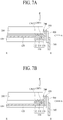
- FIGS. 7A and 7B are brief views illustrating a display device according to the fourth embodiment of the present invention, especially illustrating a side bonding contact structure taken along line II-II of FIG. 3 .
- description of the display device according to the fourth embodiment of the present invention detailed description of the same elements as those of the first embodiment may be omitted.
- the display device includes a first substrate 100, a second substrate 200, a flexible circuit film 400, and a printed circuit board (PCB) 500.
- PCB printed circuit board
- the first substrate 100 and the second substrate 200 are bonded to each other to constitute a display panel.
- the display panel includes an active area A/A where an image is displayed, and a pad area PA corresponding to a non-display area.
- the pad area PA is arranged outside the active area A/A.
- a plurality of signal pads 110 are arranged in the pad area PA, and each signal pad 110 has a multi-layer structure.
- a contact portion 130 for electrically connecting multi-layers of the plurality of signal pads 110 is arranged in the pad area PA.
- the flexible circuit film 400 and the printed circuit board 500 constitute a panel driver.
- the flexible circuit film 400 is attached to a side of the display panel, and the printed circuit board 500 is connected to the flexible circuit film 400.
- the first substrate 100 and the second substrate 200 have the same patterns as each other.
- the first substrate 100 and the second substrate 200 may have the same sized quadrangles as each other. That is, according to the fourth embodiment of the present invention, one end of the first substrate 100 is matched with one end of the second substrate 200 in an area to which the flexible circuit film 400 is attached, unlike the related art in which the first substrate 10 is more extended than the second substrate 20 in the area to which the flexible circuit film 40 is attached.
- the flexible circuit film 400 is attached to the side of the display panel without being attached to an upper surface of the first substrate 100.
- one flexible circuit film 400 and one printed circuit board 500 are connected to one side of the display panel, for example, a lower side of the display panel
- another one flexible circuit film 400 and another one printed circuit board 500 may additionally be connected to the other side of the display panel, for example, a left side of the display panel.
- the first substrate 100 and the second substrate 200 face each other, and have the same lengths as each other. Also, one end of the first substrate 100 is matched with one end of the second substrate 200, and the other end of the first substrate 100 is matched with the other end of the second substrate 200.
- the present invention is not limited to this case, and details of the first substrate 100 and the second substrate 200 may be varied depending on the display device which is used.
- a line 120 is formed on the first substrate 100, and the signal pad 110 is connected to an end of the line 120.
- the line 120 may be made of a signal line such as a gate line, a data line, or a common voltage line.
- the line 120 may be made of a non-signal line such as an electrostatic discharge line.
- FIG. 8 is a view illustrating a side bonding contact structure viewed in a direction B of FIG. 7B , especially illustrating a plurality signal pads and a plurality of lines, which are arranged on the first substrate.
- FIG. 9 is a view illustrating a side bonding contact structure viewed in a direction A of FIG. 7B , especially illustrating a section taken along a grinding line shown in FIG. 8 .
- connection electrode 300 is arranged at the side of the display panel, the connection electrode 300 is not shown in FIG. 8 .
- each of the plurality of signal pads 110 is formed in a multi-layer structure.
- the signal pad 110 includes a first line 112, a second line 114, and a third line 116.
- a first insulating film 113 is arranged between the first line 112 and the second line 114, and a second insulating film 115 is arranged between the second line 114 and the third line 116.
- a gate insulating film of an inorganic material for example, oxide silicon or nitride silicon
- a passivation film of an organic material for example, photoacryl
- the first line 112 may be arranged on the same layer as the gate line arranged in the active area A/A.
- the first line 112 may have a thickness D1 of 400nm to 500nm.
- the second line 114 may be arranged on the same layer (source/drain layer) as the data line arranged in the active area A/A.
- the second line 114 may have a thickness D2 of 400nm to 500nm.
- the first line 112 and the second line 114 are electrically connected with each other through a first contact hole CNT1.
- the third line 116 may be arranged on the same layer as the pixel electrode arranged in the active area A/A.
- the third line 116 may have a thickness D3 of 20nm to 40nm.
- the second line 114 and the third line 116 are electrically connected with each other through a second contact hole CNT2.
- first line 112, the second line 114 and the third line 116 are electrically connected with one another through the first contact hole CN1 and the second contact hole CNT2.
- the line 120 and the signal pad 110 are electrically connected with each other.
- the line 120 may be arranged on the same layer as the second line 114 of the signal pad 110 and therefore may be connected with the second line 114 in one body.
- the line 120 may be arranged on the same layer as the first line 112 of the signal pad 110 and therefore may be connected with the first line 112 in one body.
- one line constituting the signal pad 110 is formed on the same layer as the line 120 in one body as shown, the present invention is not limited to this case.
- the line 120 may be made of a data line provided on the gate insulating film
- the signal pad 110 may be made of a data pad provided below the gate insulating film.
- the data pad may be connected with the data line through a contact hole (not shown) provided in the gate insulating film.
- One end of the first substrate 100 is matched with one end of the second substrate 200 in the area where the signal pad 110 is formed. Therefore, the flexible circuit film 400 is electrically connected to one side of the signal pad 110 unlike the related art that the flexible circuit film 40 is connected to the upper surface of the signal pad 11.
- one side of the signal pad 110 which is connected to the flexible circuit film 400, has a width relatively smaller than that of the upper surface of the signal pad 110, connection property between the signal pad 110 and the flexible circuit film 400 may be deteriorated.
- the signal pad 110 is comprised of the first line 112, the second line 114 and the third line 116, whereby an area where the signal pad 110 is connected with the flexible circuit film 400 is increased.
- connection electrode 300 is formed at one side of the signal pad 110 to improve connection property between the signal pad 110 and the flexible circuit film 400.
- connection electrode 300 is formed in contact with each side of the first substrate 100 and the second substrate 200, at which the signal pad 110 is formed, and at the same time is directly connected with one side of the signal pad 110.
- the connection electrode 300 may be made of, but not limited to, Ag having excellent conductivity.
- connection electrode 300 An adhesive layer 350 is arranged between the connection electrode 300 and the flexible circuit film 400 to attach the flexible circuit film 400 to the connection electrode 300. Since the adhesive layer 350 is provided with a conductive ball therein, the connection electrode 300 may electrically be connected with the flexible circuit film 400 through the conductive ball.
- the flexible circuit film 400 is formed on the adhesive layer 350.
- the lead line is formed on the surface of the flexible circuit film 400, which faces the adhesive layer 350.
- the lead line is electrically connected with the connection electrode 300 through the conductive ball. That is, one side of the conductive ball is in contact with the connection electrode 300, and the other side of the conductive ball is in contact with the lead line.
- the printed circuit board 500 is formed on the flexible circuit film 400.
- the flexible circuit film 400 is not formed on the first substrate 100 but arranged vertically along the sides of the first substrate 100 and the second substrate 200. That is, the flexible circuit film 400 is attached to the sides of the first substrate 100 and the second substrate 200 in a manner of side bonding.
- a chip such as a driving integrated circuit may be formed on the flexible circuit film 400 to constitute a chip on film (COF) structure.
- COF chip on film
- the present invention is not limited to the COF structure.
- the lead line is provided on the flexible circuit film 400, and is connected with the connection electrode 300 through the conductive ball of the adhesive layer 350.
- the printed circuit board 500 applies various signals to the display panel through the flexible circuit film 400. Although not shown, a timing controller, various power circuits, or a memory device may be packaged on the printed circuit board 500.
- connection electrode 300 is connected with each of the plurality signal pads 110. That is, one signal pad 110 and one connection electrode 300 are connected with each other one to one.
- a width W1 of the signal pad 110 is wider than a width W2 between the signal pads.
- the width W1 of the signal pad 110 may be wider than the width W2 between the signal pads by four times. If the signal pad 110 has a width of 120 ⁇ m, the width between the signal pads may be 30 ⁇ m.
- the signal pad 110 is electrically connected with the printed circuit board 500 through the connection electrode 300, the conductive ball and the lead line.
- a unit display panel is manufactured by cutting an original plate, which is obtained by bonding the first substrate and the second substrate to each other, along a grinding line during a manufacturing process.
- the signal pad exposed at the side of the display panel may be lost, whereby a contact area between the signal pad and the connection electrode may be reduced. For this reason, a contact defect may be caused. If the contact defect of the signal pad and the connection electrode occurs, no signal is applied to the active area A/A even though a signal is applied to the signal pad, whereby a lighting defect occurs in pixels connected to a corresponding line.
- the signal pad 110 is comprised of the first line 112, the second line 114 and the third line 116, whereby a wide contact area is formed. Therefore, electrical connection between the signal pad 110 and the connection electrode 300 is excellent and physical adhesion therebetween is very excellent, whereby a connection defect caused by side processing of the display panel may be reduced.
- connection electrode 300 is connected with the signal pad 110 at the side of each of the first substrate 100 and the second substrate 200, and the flexible circuit film 400 is attached to the connection electrode 300 at the sides of the first substrate 100 and the second substrate 200, whereby the first substrate 100 may not be required to be more extended than the second substrate 200 to expose the upper surface of the signal pad 100 like the related art.
- a bezel area is reduced as compared with the related art. Also, since one end and the other end of the first substrate 100 are matched with those of the second substrate 200, it is advantageous that a step difference is prevented from being generated in the bezel area. Particularly, since the signal pad 110 is comprised of the first line 112, the second line 114 and the third line 116 to form a wide contact area, electrical connection and physical adhesion may be improved even though a side bonding contact structure is used.
- FIG. 10 is a brief cross-sectional view illustrating a display device according to the fifth embodiment of the present invention.
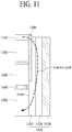
- FIG. 11 is an enlarged view illustrating a portion A shown in FIG. 10 .
- the display device 1000 includes a display panel comprised of a first substrate 1100 and a second substrate 1200, a ground electrode 1300, a conductive light-shielding portion 1400, a metal frame 1500, and an elastic resin 1600.
- the first substrate 1100 and the second substrate 1200 are bonded to each other to constitute a display panel.
- a flexible circuit film 400 and a printed circuit board (not shown) constitute a panel driver.
- An electrostatic discharge layer 1240 is arranged on the display panel, and an upper polarizing film 1220 is arranged on the electrostatic discharge layer 1240.
- a lower polarizing film 1120 is arranged below the display panel.
- the metal frame 1500 has a quadrangle box shape of which upper surface is opened, and has four inner sides inclined at a certain angle.
- the metal frame 1500 has a wide lower surface but a width is reduced toward an upper surface.
- the elastic resin 1600 is arranged on the metal frame 1500, and the display panel is mounted on the elastic resin 1600.
- the elastic resin 1600 has adhesion to fix the display panel onto the metal frame 1500.
- the elastic resin 1600 has a predetermined elastic force to prevent the display panel from being damaged by impact.
- the flexible circuit film 400 is attached to the side of the display panel, and the printed circuit board is connected to the flexible circuit film 400.
- a connection structure between the flexible circuit film 400 and the printed circuit board is shown in FIGS. 3 to 9 , and its detailed description will be made with reference to these drawings.
- the first substrate 1100 and the second substrate 1200 have the same patterns as each other.
- the first substrate 1100 and the second substrate 1200 may have the same sized quadrangles as each other. That is, according to the fifth embodiment of the present invention, one end of the first substrate 1100 is matched with one end of the second substrate 1200 in an area to which the flexible circuit film 400 is attached. That is, according to the related art, the first substrate 10 is more extended than the second substrate 20 in the area to which the flexible circuit film 40 is attached. However, in the present invention, the first substrate 1100 is not more extended than the second substrate 1200 in the area to which the circuit flexible film 400 is attached.
- the flexible circuit film 400 is attached to the side of the display panel without being attached to an upper surface of the first substrate 1100.
- FIG. 12A is a view illustrating a side bonding contact structure and an electrostatic discharge (ESD) structure, which are viewed in a direction B of FIG. 10 .
- FIG. 12B is a view illustrating that a conductive light shielding portion is attached to a side of a display panel.
- a plurality of signal pads are formed on the first substrate 1100, and a plurality of connection electrodes 300 are arranged to cover each of the plurality of signal pads. Since each connection electrode 300 covers each signal pad, the plurality of signal pads are not shown in FIGS. 12A and 12B .
- a shape and an arrangement structure of the plurality of signal pads are shown in FIGS. 3 to 9 , and their detailed description will be made with reference to these drawings.
- the plurality of signal pads include a gate pad, a data pad, an electrostatic discharge pad, and a common voltage pad.
- Various modifications known in the art may be made in a type and arrangement of the signal pads.
- connection electrode 300 is connected to each of the signal pads. That is, one signal pad and one connection electrode 300 are connected to each other one to one.
- the connection electrode 300 is electrically connected with a lead line 420 formed on the flexible circuit film 400, and the lead line 420 is connected with the printed circuit board.
- the flexible circuit film 400 is attached to sides of the first substrate 1100 and the second substrate 1200 through a conductive adhesive layer, and the lead line 420 of the flexible circuit film 400 is electrically connected with the connection electrode 300 through a conductive ball included in the conductive adhesive layer.
- the electrostatic discharge pad of the plurality of signal pads is connected with an ESD pad 430 arranged in the flexible circuit film 400.
- the ESD pad 430 is connected with an electrostatic discharge layer 1240 formed on the second substrate 1200 through a ground line 410.
- the electrostatic discharge layer 1240 provided on the second substrate 1200 is electrically connected with the electrostatic discharge pad through the ground line 410.
- a plurality of ground electrodes 1300 are arranged at one side of the display panel.
- the plurality of ground electrodes 1300 are connected with the electrostatic discharge layer 1240 formed on the second substrate 1200.
- the electrostatic discharge layer 1240 provided on the second substrate 1200 is electrically connected with the plurality of ground electrodes 1300.
- the ground electrode 1300 may be made of, but not limited to, Ag having excellent conductivity.
- a conductive light-shielding portion 1400 is arranged to cover the plurality of ground electrodes 1300 electrically connected with the electrostatic discharge layer provided on the second substrate 1200, the side of the first substrate 1100 and the side of the second substrate 1200.
- the conductive light-shielding portion 1400 is arranged on the flexible circuit film 400, the flexible circuit film 400 is insulated from the conductive light-shielding portion by an insulating film 440. Therefore, the flexible circuit film 400 is insulated from the plurality of ground electrodes 1300.
- the conductive light-shielding portion 1400 is obtained by mixing a conductive metal material with an adhesive material, and is attached to the plurality of ground electrodes 1300 and an outer sidewall 1510 of the metal frame 1500 and therefore the plurality of ground electrodes 1300 are electrically connected with the metal frame 1500.
- the conductive light-shielding portion 1400 includes a conductive adhesive layer 1410 attached to the outer sidewall 1510 of the metal frame 1500 and the plurality of ground electrodes 1300, a metal film 1420 arranged on the conductive adhesive layer 1410, and a light-shielding film 1430 arranged on the metal film 1420, and is arranged to cover the flexible circuit film 400. Also, the conductive adhesive layer 1410 is also attached onto the flexible circuit film 400 to fix the flexible circuit film 400.
- the metal film 1420 may be made of a metal material such as Al or Cu, which has excellent conductivity. As shown from the current path in FIG. 11 , static electricity generated from the electrostatic discharge layer 1240 enters the plurality of ground electrodes 1300 and then is discharged to the metal frame 1500 through the metal film 1420.
- a light-shielding film 1430 prevents external light from entering the display device 1000 and also prevents light leakage from occurring in a joint portion of the display device 1000. Also, the light-shielding film 1430 is attached to the side of the display device 1000, whereby esthetic appearance of the display device 1000 is improved.
- the flexible circuit film 400 is attached to the side of the display panel by the side bonding manner, and the electrostatic discharge (ESD) structure may be arranged at the side of the display panel to reduce a bezel.
- ESD electrostatic discharge
- static electricity generated on the electrostatic discharge layer 1240 may effectively be removed through the plurality of ground electrodes 1300.
- appearance of the display device may be improved, and the manufacturing process may be simplified and the manufacturing cost may be reduced.
- FIG. 13 is a view illustrating a video wall display device constituted by arranging display devices according to the first to fifth embodiments of the present invention in a tile pattern.
- four(4) display devices DP1 to DP4 according to the first to fifth embodiments of the present invention are arranged in a tile pattern of 2 ⁇ 2 to constitute a video wall display device 2000.
- the video wall display device 2000 is formed by combination of the plurality of display devices DP1 to DP4, esthetic appearance of the video wall display device is deteriorated if a bezel of each of the display devices DP1 to DP4 is increased. Particularly, intervals among the display devices DP1 to DP4 become wide, whereby an image is not displayed smoothly, whereby a problem occurs in that display quality is deteriorated.
- Side bonding may be applied to the display device according to the first to fifth embodiments of the present invention as described above to reduce a bezel, whereby esthetic appearance may be improved when the display device according to the present invention is applied to the video wall display device 2000. Also, since the intervals among the display devices DP1 to DP4 may be formed to become narrow, image may be displayed smoothly, whereby display quality of the video wall display device 2000 may be improved.
- the display device of the present invention comprises a display panel including an active area where an image is displayed and a pad area corresponding to a non-display area, the display device comprising a first substrate and a second substrate which face each other and are bonded to each other to constitute the display panel.
- a signal pad is arranged on the first substrate, and a connection electrode is connected with one side of the signal pad.
- a flexible circuit film connected with the connection electrode is arranged.
- the signal pad includes a plurality of lines arranged by interposing an insulating film therebetween, wherein the plurality of lines are electrically connected with each other.
- the plurality of lines of the signal pad include at least two lines of a first line arranged on the same layer as a gate line arranged in the active area, a second line arranged on the same layer as a data line arranged in the active area, and a third line arranged on the same layer as a pixel electrode arranged in the active area.
- a first insulating film is arranged between the first line and the second line, the first line and the second line are electrically connected with each other through a first contact hole, a second insulating film is arranged between the second line and the third line, and the second line and the third line are electrically connected with each other through a second contact hole.
- connection electrode is arranged at a side of the first substrate and a side of the second substrate.
- the first line and the second line are electrically connected with the connection electrode at one side of each of the first substrate and the second substrate.
- the first line and the third line are electrically connected with the connection electrode at one side of each of the first substrate and the second substrate.
- the second line and the third line are electrically connected with the connection electrode at one side of each of the first substrate and the second substrate.
- the first line, the second line and the third line are electrically connected with the connection electrode at one side of each of the first substrate and the second substrate.
- the flexible circuit film is arranged at the side of the first substrate and the side of the second substrate by an adhesive layer.
- the display device of the present invention may further comprise an electrostatic discharge layer arranged on the second substrate, and a plurality of ground electrodes electrically connected with the electrostatic discharge layer and arranged at the side of the first substrate and the side of the second substrate.
- the display device of the present invention may further comprise a metal frame on which the first substrate and the second substrate are mounted, and a conductive light-shielding portion arranged to cover the plurality of ground electrodes, the side of the first substrate and the side of the second substrate.
- the conductive light-shielding portion is attached to an external sidewall of the metal frame, whereby the plurality of ground electrodes are electrically connected with the metal frame.
- the conductive light-shielding portion includes a conductive adhesive layer attached to the outer sidewall of the metal frame and the plurality of ground electrodes, a metal film arranged on the conductive adhesive layer, and a light-shielding film arranged on the metal film.
- the conductive light-shielding portion is arranged to cover the flexible circuit film.
- connection electrode is connected with one side of the pad at the side of each of the first substrate and the second substrate, and therefore the flexible circuit film may be attached to the side of each of the first substrate and the second substrate, whereby the first substrate may not be required to be more extended than the second substrate to expose the upper surface of the pad like the related art. Therefore, according to the present invention, it is advantageous that a bezel area is reduced as compared with the related art.
- connection electrode is connected with the signal pad at the side of each of the first substrate and the second substrate, and the flexible circuit film is attached to the connection electrode at the sides of the first substrate and the second substrate, whereby the first substrate may not be required to be more extended than the second substrate to expose the upper surface of the signal pad like the related art.
- the signal pad is connected with the connection electrode by the side bonding manner, whereby it is advantageous that the bezel area is reduced as compared with the related art.
- the signal pad is comprised of the first line, the second line and even the third line to form a wide contact area, electrical connection and physical adhesion may be improved even though a side bonding contact structure is used.
- the flexible circuit film may be attached to the side of the display panel by the side bonding manner, and the electrostatic discharge (ESD) structure may be arranged at the side of the display panel to reduce a bezel.
- ESD electrostatic discharge
- static electricity generated on the electrostatic discharge layer may effectively be removed through the plurality of ground electrodes.
- appearance of the display device may be improved, and the manufacturing process may be simplified and the manufacturing cost may be reduced.
- Side bonding may be applied to the display device according to the first to fifth embodiments of the present invention to reduce a bezel, whereby esthetic appearance may be improved when the display device according to the present invention is applied to the video wall display device.
- intervals among the display devices may be formed to become narrow, image may be displayed smoothly, whereby display quality of the video wall display device may be improved.
Landscapes
- Physics & Mathematics (AREA)
- Nonlinear Science (AREA)
- General Physics & Mathematics (AREA)
- Optics & Photonics (AREA)
- Crystallography & Structural Chemistry (AREA)
- Chemical & Material Sciences (AREA)
- Mathematical Physics (AREA)
- Engineering & Computer Science (AREA)
- Microelectronics & Electronic Packaging (AREA)
- Devices For Indicating Variable Information By Combining Individual Elements (AREA)
- Power Engineering (AREA)
- Theoretical Computer Science (AREA)
- Liquid Crystal (AREA)
Claims (15)
- Dispositif d'affichage comportant une aire de surface active (A/A) pour afficher une image, le dispositif d'affichage comportant :un premier substrat (100, 1100) ;une pastille de signal (110) ayant une structure multicouche et étant disposée sur le premier substrat (100, 1100) ;une électrode de connexion (300) formée sur une surface latérale du premier substrat (100, 1100) perpendiculaire à une surface de l'aire de surface active (A/A) du dispositif d'affichage et reliée à la pastille de signal à structure multicouche (110) ; etun film de circuit souple (400) relié à l'électrode de connexion (300),dans lequel la pastille de signal à structure multicouche (110) inclut au moins deux lignes (112, 114, 116) superposées l'une sur l'autre avec au moins un film isolant (113, 115) intercalé entre celles-ci, dans lequel les lignes (112, 114, 116) sont respectivement reliées électriquement à l'électrode de connexion (300) sur la surface latérale du premier substrat (100, 1100), et dans lequel les au moins deux lignes (112, 114, 116) sont électriquement reliées l'une à l'autre via au moins un trou de contact (CNT1, CNT2) pénétrant dans le film isolant (113, 115).
- Dispositif d'affichage selon la revendication 1, comportant en outre :un second substrat (200, 1200) dirigé vers le premier substrat (100, 1100) ;dans lequel l'électrode de connexion (300) est formée sur la surface latérale du premier substrat (100, 1100) et du second substrat (200, 1200) et reliée à la pastille de signal (110),dans lequel la pastille de signal (110) inclut au moins deux lignes (112, 114, 116) superposées l'une sur l'autre avec au moins un film isolant (113, 115) intercalé entre celles-ci, dans lequel les au moins deux lignes (112, 114, 116) sont électriquement reliées l'une à l'autre via au moins un trou de contact (CNT1, CNT2) pénétrant dans le film isolant (113, 115),dans lequel les au moins deux lignes (112, 114, 116) sont respectivement reliées électriquement à l'électrode de connexion (300) sur la surface latérale du premier substrat (100, 1100) et du second substrat (200, 1200).
- Dispositif d'affichage selon la revendication 2, dans lequel la pluralité de lignes (112, 114, 116) inclut au moins deux lignes parmi : une première ligne (112) disposée sur la même couche qu'une ligne de grille disposée dans l'aire de surface active (A/A), une deuxième ligne (114) disposée sur la même couche qu'une ligne de données disposée dans l'aire de surface active (A/A), et une troisième ligne (116) disposée sur la même couche qu'une électrode de pixel disposée dans l'aire de surface active (A/A).
- Dispositif d'affichage selon la revendication 3, dans lequel un premier film isolant (113) est disposé entre la première ligne (112) et la deuxième ligne (114), et la première ligne (112) et la deuxième ligne (114) sont électriquement reliées l'une à l'autre via un premier trou de contact (CNT1) dans le premier film isolant (113), et/ou dans lequel un second film isolant (115) est disposé entre la deuxième ligne (114) et la troisième ligne (116), et la deuxième ligne (114) et la troisième ligne (116) sont électriquement reliées l'une à l'autre via un second trou de contact (CNT2) dans le second film isolant (115).
- Dispositif d'affichage selon l'une quelconque des revendications 2 à 4 précédentes, dans lequel l'électrode de connexion (300) est reliée à la pastille de signal (110) sur la surface latérale du premier substrat (100, 1100) et du second substrat (200, 1200) perpendiculairement à une surface de l'aire de surface active (A/A) du dispositif d'affichage.
- Dispositif d'affichage selon l'une quelconque des revendications 2 à 5 précédentes, dans lequel les lignes de la pluralité de lignes (112, 114, 116) sont respectivement reliées électriquement à l'électrode de connexion (300) sur la surface latérale du premier substrat (100, 1100) et du second substrat (200, 1200) perpendiculairement à une surface de l'aire de surface active (A/A) du dispositif d'affichage.
- Dispositif d'affichage selon l'une quelconque des revendications 2 à 6 précédentes, dans lequel le film de circuit souple (400) est relié à l'électrode de connexion (300) par une couche adhésive (350) sur le côté du premier substrat (100, 1100) et du second substrat (200, 1200) perpendiculairement à une surface de l'aire de surface active (A/A) du dispositif d'affichage.
- Dispositif d'affichage selon l'une quelconque des revendications 2 à 7 précédentes, dans lequel le dispositif d'affichage inclut au moins une ligne parmi une ligne de grille, une ligne de données et une ligne de tension commune et une ligne de la pluralité de lignes (112, 114, 116) de la pastille de signal (110) est reliée à une ligne parmi la ligne de grille, la ligne de données et la ligne de tension commune.
- Dispositif d'affichage selon l'une quelconque des revendications 2 à 8 précédentes, dans lequel le au moins un film isolant (113, 115) inclut un film isolant de grille et/ou un film de passivation.
- Dispositif d'affichage selon l'une quelconque des revendications 2 à 9 précédentes, comportant en outre :une couche de décharge électrostatique (1240) sur le second substrat (1200) ; etune pluralité d'électrodes de masse (1300) électriquement reliées à la couche de décharge électrostatique (1240) et disposées sur le côté du premier substrat (1100) et du second substrat (1100) perpendiculairement à une surface de l'aire de surface active (A/A) du dispositif d'affichage.
- Dispositif d'affichage selon la revendication 10, comportant en outre :un châssis métallique (1500) sur lequel le premier substrat (1100) est monté ; etune partie pare-lumière conductrice (1400) sur la pluralité d'électrodes de masse (1300) et une paroi latérale (1510) du châssis métallique (1500),dans lequel la partie pare-lumière conductrice (1400) relie électriquement la pluralité d'électrodes de masse (1300) au châssis métallique (1500).
- Dispositif d'affichage selon la revendication 11, dans lequel la partie pare-lumière conductrice (1400) est disposée sur le film de circuit souple (400) avec un film isolant (440) entre les deux pour isoler le film de circuit souple (400) des électrodes de masse (1300).
- Dispositif d'affichage selon la revendication 11 ou 12, dans lequel la partie pare-lumière conductrice (1400) inclut une couche adhésive conductrice (1410) fixée à la paroi latérale (1510) du châssis métallique (1500) et à la pluralité d'électrodes de masse (1300), un film métallique (1420) disposé sur la couche adhésive conductrice (1410), et un film pare-lumière (1430) disposé sur le film métallique (1420).
- Dispositif d'affichage selon l'une quelconque des revendications 2 à 13 précédentes, dans lequel au moins un élément parmi l'électrode de connexion (300) et le film de circuit souple (400) s'étend perpendiculairement à au moins un élément parmi l'aire de surface active (A/A), les premier et second substrats (100, 200 ; 1100, 1200) et la pastille de signal.
- Dispositif d'affichage vidéo mural, incluant une pluralité de dispositifs d'affichage selon l'une quelconque des revendications précédentes, dans lequel les dispositifs d'affichage sont disposés adjacentes les uns aux autres selon un motif de mosaïque.
Applications Claiming Priority (1)
| Application Number | Priority Date | Filing Date | Title |
|---|---|---|---|
| KR1020150095395A KR102387880B1 (ko) | 2015-07-03 | 2015-07-03 | 디스플레이 장치 |
Publications (2)
| Publication Number | Publication Date |
|---|---|
| EP3112931A1 EP3112931A1 (fr) | 2017-01-04 |
| EP3112931B1 true EP3112931B1 (fr) | 2019-12-18 |
Family
ID=56360203
Family Applications (1)
| Application Number | Title | Priority Date | Filing Date |
|---|---|---|---|
| EP16177157.1A Active EP3112931B1 (fr) | 2015-07-03 | 2016-06-30 | Dispositif d'affichage |
Country Status (4)
| Country | Link |
|---|---|
| US (2) | US9947652B2 (fr) |
| EP (1) | EP3112931B1 (fr) |
| KR (2) | KR102387880B1 (fr) |
| CN (1) | CN106324927B (fr) |
Families Citing this family (61)
| Publication number | Priority date | Publication date | Assignee | Title |
|---|---|---|---|---|
| KR102378891B1 (ko) * | 2015-09-18 | 2022-03-24 | 엘지디스플레이 주식회사 | 디스플레이 패널 및 이를 포함하는 디스플레이 장치 |
| KR102626385B1 (ko) | 2016-06-08 | 2024-01-19 | 삼성디스플레이 주식회사 | 표시장치 및 이의 제조방법 |
| JP6956475B2 (ja) * | 2016-09-28 | 2021-11-02 | エルジー ディスプレイ カンパニー リミテッド | 電子部品の実装方法、電子部品の接合構造、基板装置、ディスプレイ装置、ディスプレイシステム |
| JP6726070B2 (ja) | 2016-09-28 | 2020-07-22 | エルジー ディスプレイ カンパニー リミテッド | 電子部品の実装方法、電子部品の接合構造、基板装置、ディスプレイ装置、ディスプレイシステム |
| KR102772195B1 (ko) * | 2017-02-28 | 2025-02-26 | 삼성디스플레이 주식회사 | 표시 장치 및 표시 장치의 제조 방법 |
| KR102473541B1 (ko) | 2017-04-25 | 2022-12-02 | 삼성디스플레이 주식회사 | 표시 장치 |
| TWI621900B (zh) * | 2017-04-28 | 2018-04-21 | 友達光電股份有限公司 | 顯示裝置與其製作方法 |
| KR102350908B1 (ko) * | 2017-06-12 | 2022-01-14 | 삼성디스플레이 주식회사 | 표시 장치 |
| CN107145015B (zh) * | 2017-06-30 | 2020-08-07 | 武汉华星光电技术有限公司 | 一种显示面板 |
| KR102408902B1 (ko) * | 2017-08-16 | 2022-06-15 | 엘지디스플레이 주식회사 | 디스플레이 장치 |
| CN109426018A (zh) * | 2017-08-22 | 2019-03-05 | 京东方科技集团股份有限公司 | 基板及其制造方法、显示面板、拼接屏 |
| CN107402466B (zh) * | 2017-08-31 | 2021-01-26 | Tcl华星光电技术有限公司 | 液晶显示面板的邦定方法与液晶显示面板邦定结构 |
| KR102413716B1 (ko) | 2017-09-25 | 2022-06-28 | 삼성디스플레이 주식회사 | 표시패널 |
| CN107703663A (zh) * | 2017-09-26 | 2018-02-16 | 张家港康得新光电材料有限公司 | 2d/3d可切换面板及显示装置 |
| CN107643634A (zh) * | 2017-10-26 | 2018-01-30 | 深圳市华星光电半导体显示技术有限公司 | 一种像素单元及显示基板 |
| KR102433358B1 (ko) * | 2017-12-05 | 2022-08-16 | 엘지디스플레이 주식회사 | 표시 장치 |
| KR102456493B1 (ko) * | 2017-12-21 | 2022-10-20 | 삼성디스플레이 주식회사 | 표시장치 |
| KR102464097B1 (ko) * | 2017-12-28 | 2022-11-07 | 삼성디스플레이 주식회사 | 표시 장치 |
| KR20190083027A (ko) * | 2018-01-02 | 2019-07-11 | 삼성디스플레이 주식회사 | 표시패널 및 그 제조방법 |
| US11018174B2 (en) * | 2018-01-22 | 2021-05-25 | Semiconductor Components Industries, Llc | Apparatus and method related to sensor die ESD protection |
| CN108957878B (zh) * | 2018-07-19 | 2022-03-11 | 武汉天马微电子有限公司 | 显示模组及其制备方法和显示装置 |
| KR102731395B1 (ko) * | 2018-08-14 | 2024-11-18 | 삼성디스플레이 주식회사 | 표시장치 및 그 제조방법 |
| KR102606567B1 (ko) * | 2018-11-07 | 2023-11-28 | 삼성디스플레이 주식회사 | 유기 발광 표시 장치 |
| KR102657409B1 (ko) * | 2018-12-20 | 2024-04-16 | 엘지디스플레이 주식회사 | 표시패널 및 표시장치 |
| KR102713260B1 (ko) * | 2018-12-26 | 2024-10-04 | 삼성디스플레이 주식회사 | 표시 장치 |
| KR102743289B1 (ko) * | 2018-12-28 | 2024-12-17 | 엘지디스플레이 주식회사 | 표시장치 |
| KR102605376B1 (ko) | 2018-12-31 | 2023-11-23 | 삼성디스플레이 주식회사 | 표시 장치 |
| TWI685828B (zh) * | 2019-01-03 | 2020-02-21 | 友達光電股份有限公司 | 顯示裝置 |
| KR102608963B1 (ko) * | 2019-03-19 | 2023-12-05 | 삼성디스플레이 주식회사 | 표시 장치 및 이의 제조 방법 |
| KR102768192B1 (ko) * | 2019-03-25 | 2025-02-14 | 삼성디스플레이 주식회사 | 표시 장치 및 그 제조 방법 |
| CN110119054B (zh) * | 2019-04-25 | 2022-02-22 | Tcl华星光电技术有限公司 | 显示面板 |
| EP3918635A4 (fr) | 2019-05-03 | 2022-04-06 | Samsung Electronics Co., Ltd. | Module de diode électroluminescente |
| KR20200127815A (ko) * | 2019-05-03 | 2020-11-11 | 삼성전자주식회사 | 발광 다이오드 모듈 및 이를 포함하는 디스플레이 장치 |
| KR102939374B1 (ko) * | 2019-06-28 | 2026-03-17 | 삼성디스플레이 주식회사 | 표시 장치 및 그 제조 방법 |
| KR102870807B1 (ko) | 2019-07-22 | 2025-10-14 | 삼성디스플레이 주식회사 | 표시 장치 |
| KR102807945B1 (ko) * | 2019-09-02 | 2025-05-15 | 삼성디스플레이 주식회사 | 표시 장치 |
| KR102787781B1 (ko) | 2019-10-07 | 2025-03-27 | 삼성디스플레이 주식회사 | 표시 장치 |
| CN110764295A (zh) * | 2019-10-14 | 2020-02-07 | 深圳市华星光电半导体显示技术有限公司 | 液晶显示面板及液晶模组 |
| CN110837194B (zh) * | 2019-10-30 | 2022-04-26 | 深圳市华星光电半导体显示技术有限公司 | 一种液晶显示装置、拼接屏 |
| CN110718156B (zh) * | 2019-10-31 | 2022-08-19 | 京东方科技集团股份有限公司 | 可折叠显示面板及制作方法、显示装置 |
| KR102839526B1 (ko) * | 2019-11-06 | 2025-07-25 | 주식회사 엘엑스글라스 | 유리 조립체 |
| KR20210073649A (ko) * | 2019-12-10 | 2021-06-21 | 삼성디스플레이 주식회사 | 유기 발광 표시 장치 및 유기 발광 표시 장치의 제조 방법 |
| KR102945401B1 (ko) * | 2019-12-19 | 2026-03-31 | 삼성디스플레이 주식회사 | 표시 장치 |
| KR20210109087A (ko) | 2020-02-26 | 2021-09-06 | 삼성디스플레이 주식회사 | 표시 장치 |
| KR102748338B1 (ko) * | 2020-03-27 | 2025-01-02 | 삼성디스플레이 주식회사 | 본딩 장치 및 그것을 이용한 표시 장치의 제조 방법 |
| CN113823185B (zh) * | 2020-06-19 | 2023-09-12 | 群创光电股份有限公司 | 电子装置 |
| KR102914090B1 (ko) * | 2020-07-03 | 2026-01-19 | 삼성디스플레이 주식회사 | 표시장치 |
| MY199608A (en) * | 2020-07-31 | 2023-11-09 | Samsung Electronics Co Ltd | Electronic device including conductive member |
| CN113674614B (zh) * | 2020-08-14 | 2023-03-21 | 友达光电股份有限公司 | 显示装置及其制造方法 |
| CN113284416B (zh) * | 2020-08-14 | 2023-03-10 | 友达光电股份有限公司 | 显示面板 |
| KR102887784B1 (ko) * | 2020-10-27 | 2025-11-19 | 삼성전자주식회사 | 디스플레이 장치 및 이의 제조방법 |
| CN114582220B (zh) * | 2020-11-30 | 2025-04-29 | 京东方科技集团股份有限公司 | 显示母板及其制造方法、显示基板、显示面板 |
| US11515271B2 (en) * | 2021-01-27 | 2022-11-29 | Innolux Corporation | Electronic device including wire on side surface of substrate and manufacturing method thereof |
| CN114815407B (zh) * | 2021-01-28 | 2024-08-27 | 京东方科技集团股份有限公司 | 显示基板及其制备方法、显示面板 |
| CN115145065B (zh) * | 2021-03-31 | 2025-04-08 | 京东方科技集团股份有限公司 | 显示面板及其制备方法、显示装置和拼接显示装置 |
| EP4332948A4 (fr) * | 2021-10-27 | 2024-11-06 | Samsung Electronics Co., Ltd. | Dispositif d'affichage comprenant un module d'affichage et procédé de fabrication associé |
| CN115036329B (zh) * | 2022-04-15 | 2025-05-02 | 合肥京东方显示技术有限公司 | 一种显示基板、显示基板的制作方法及显示装置 |
| US11662861B1 (en) * | 2022-04-29 | 2023-05-30 | Dell Products L.P. | Edge display having electrostatic discharge protection |
| CN114935858A (zh) * | 2022-05-26 | 2022-08-23 | Tcl华星光电技术有限公司 | 液晶显示装置及其制造方法 |
| CN116110927B (zh) * | 2023-03-28 | 2025-07-22 | 天马新型显示技术研究院(厦门)有限公司 | 显示面板和显示装置 |
| KR20250128684A (ko) * | 2024-02-21 | 2025-08-28 | 엘지디스플레이 주식회사 | 표시 장치 |
Family Cites Families (10)
| Publication number | Priority date | Publication date | Assignee | Title |
|---|---|---|---|---|
| JP2006047827A (ja) * | 2004-08-06 | 2006-02-16 | Mitsubishi Electric Corp | 液晶表示装置およびその製造方法 |
| KR20080024826A (ko) * | 2006-09-15 | 2008-03-19 | 삼성전자주식회사 | 액정표시장치 |
| KR101800013B1 (ko) * | 2010-10-29 | 2017-11-22 | 엘지디스플레이 주식회사 | 전기영동 표시장치 |
| US20150177542A1 (en) * | 2012-11-29 | 2015-06-25 | Kyocera Corporation | Display apparatus |
| KR101931248B1 (ko) * | 2012-12-27 | 2019-03-13 | 엘지디스플레이 주식회사 | 표시장치 및 그 제조방법 |
| KR102060665B1 (ko) * | 2013-05-20 | 2019-12-30 | 엘지전자 주식회사 | 디스플레이 패널 및 그를 포함하는 디스플레이 장치 |
| US8994042B2 (en) * | 2013-05-20 | 2015-03-31 | Lg Electronics Inc. | Display panel and display device |
| KR102113607B1 (ko) * | 2013-08-30 | 2020-05-21 | 엘지디스플레이 주식회사 | 액정 표시 장치 및 그의 제조 방법 |
| KR102145961B1 (ko) * | 2013-12-18 | 2020-08-20 | 삼성디스플레이 주식회사 | 유기 발광 표시 장치 |
| CN103700782B (zh) * | 2013-12-26 | 2015-12-09 | 合肥京东方光电科技有限公司 | 一种oled显示面板及其制备方法 |
-
2015
- 2015-07-03 KR KR1020150095395A patent/KR102387880B1/ko active Active
-
2016
- 2016-06-30 EP EP16177157.1A patent/EP3112931B1/fr active Active
- 2016-07-01 US US15/200,787 patent/US9947652B2/en active Active
- 2016-07-01 CN CN201610512128.5A patent/CN106324927B/zh active Active
-
2018
- 2018-03-06 US US15/913,478 patent/US10170462B2/en active Active
-
2022
- 2022-04-13 KR KR1020220045787A patent/KR102522555B1/ko active Active
Non-Patent Citations (1)
| Title |
|---|
| None * |
Also Published As
| Publication number | Publication date |
|---|---|
| KR102522555B1 (ko) | 2023-04-14 |
| KR102387880B1 (ko) | 2022-04-18 |
| KR20170005341A (ko) | 2017-01-12 |
| KR20220052884A (ko) | 2022-04-28 |
| CN106324927B (zh) | 2019-11-29 |
| US9947652B2 (en) | 2018-04-17 |
| CN106324927A (zh) | 2017-01-11 |
| US10170462B2 (en) | 2019-01-01 |
| US20180197849A1 (en) | 2018-07-12 |
| EP3112931A1 (fr) | 2017-01-04 |
| US20170005083A1 (en) | 2017-01-05 |
Similar Documents
| Publication | Publication Date | Title |
|---|---|---|
| EP3112931B1 (fr) | Dispositif d'affichage | |
| US10663816B2 (en) | Display device and method of manufacturing the same | |
| US10203573B2 (en) | Display device | |
| US10861371B2 (en) | Display device | |
| TWI638211B (zh) | Display device | |
| US11189682B2 (en) | Display device and method of manufacturing the same | |
| US9798206B2 (en) | Liquid crystal display apparatus | |
| US8767161B2 (en) | Display device | |
| KR102522706B1 (ko) | 표시 장치 | |
| JP2007024963A (ja) | 液晶表示装置 | |
| JP2011002609A (ja) | 横電界方式の液晶表示装置 | |
| KR102227163B1 (ko) | 표시 장치 | |
| US12514044B2 (en) | Display device having a reduced bezel | |
| JP2007024964A (ja) | 液晶表示装置 | |
| JP2021043420A (ja) | 表示装置 | |
| JP2010181544A (ja) | 表示素子 |
Legal Events
| Date | Code | Title | Description |
|---|---|---|---|
| PUAI | Public reference made under article 153(3) epc to a published international application that has entered the european phase |
Free format text: ORIGINAL CODE: 0009012 |
|
| STAA | Information on the status of an ep patent application or granted ep patent |
Free format text: STATUS: REQUEST FOR EXAMINATION WAS MADE |
|
| 17P | Request for examination filed |
Effective date: 20160630 |
|
| AK | Designated contracting states |
Kind code of ref document: A1 Designated state(s): AL AT BE BG CH CY CZ DE DK EE ES FI FR GB GR HR HU IE IS IT LI LT LU LV MC MK MT NL NO PL PT RO RS SE SI SK SM TR |
|
| AX | Request for extension of the european patent |
Extension state: BA ME |
|
| RBV | Designated contracting states (corrected) |
Designated state(s): AL AT BE BG CH CY CZ DE DK EE ES FI FR GB GR HR HU IE IS IT LI LT LU LV MC MK MT NL NO PL PT RO RS SE SI SK SM TR |
|
| STAA | Information on the status of an ep patent application or granted ep patent |
Free format text: STATUS: EXAMINATION IS IN PROGRESS |
|
| 17Q | First examination report despatched |
Effective date: 20181011 |
|
| GRAP | Despatch of communication of intention to grant a patent |
Free format text: ORIGINAL CODE: EPIDOSNIGR1 |
|
| STAA | Information on the status of an ep patent application or granted ep patent |
Free format text: STATUS: GRANT OF PATENT IS INTENDED |
|
| INTG | Intention to grant announced |
Effective date: 20190712 |
|
| GRAS | Grant fee paid |
Free format text: ORIGINAL CODE: EPIDOSNIGR3 |
|
| GRAA | (expected) grant |
Free format text: ORIGINAL CODE: 0009210 |
|
| STAA | Information on the status of an ep patent application or granted ep patent |
Free format text: STATUS: THE PATENT HAS BEEN GRANTED |
|
| AK | Designated contracting states |
Kind code of ref document: B1 Designated state(s): AL AT BE BG CH CY CZ DE DK EE ES FI FR GB GR HR HU IE IS IT LI LT LU LV MC MK MT NL NO PL PT RO RS SE SI SK SM TR |
|
| REG | Reference to a national code |
Ref country code: CH Ref legal event code: EP |
|
| REG | Reference to a national code |
Ref country code: IE Ref legal event code: FG4D |
|
| REG | Reference to a national code |
Ref country code: DE Ref legal event code: R096 Ref document number: 602016026266 Country of ref document: DE |
|
| REG | Reference to a national code |
Ref country code: AT Ref legal event code: REF Ref document number: 1215269 Country of ref document: AT Kind code of ref document: T Effective date: 20200115 |
|
| REG | Reference to a national code |
Ref country code: NL Ref legal event code: FP |
|
| PG25 | Lapsed in a contracting state [announced via postgrant information from national office to epo] |
Ref country code: LV Free format text: LAPSE BECAUSE OF FAILURE TO SUBMIT A TRANSLATION OF THE DESCRIPTION OR TO PAY THE FEE WITHIN THE PRESCRIBED TIME-LIMIT Effective date: 20191218 Ref country code: SE Free format text: LAPSE BECAUSE OF FAILURE TO SUBMIT A TRANSLATION OF THE DESCRIPTION OR TO PAY THE FEE WITHIN THE PRESCRIBED TIME-LIMIT Effective date: 20191218 Ref country code: FI Free format text: LAPSE BECAUSE OF FAILURE TO SUBMIT A TRANSLATION OF THE DESCRIPTION OR TO PAY THE FEE WITHIN THE PRESCRIBED TIME-LIMIT Effective date: 20191218 Ref country code: NO Free format text: LAPSE BECAUSE OF FAILURE TO SUBMIT A TRANSLATION OF THE DESCRIPTION OR TO PAY THE FEE WITHIN THE PRESCRIBED TIME-LIMIT Effective date: 20200318 Ref country code: BG Free format text: LAPSE BECAUSE OF FAILURE TO SUBMIT A TRANSLATION OF THE DESCRIPTION OR TO PAY THE FEE WITHIN THE PRESCRIBED TIME-LIMIT Effective date: 20200318 Ref country code: LT Free format text: LAPSE BECAUSE OF FAILURE TO SUBMIT A TRANSLATION OF THE DESCRIPTION OR TO PAY THE FEE WITHIN THE PRESCRIBED TIME-LIMIT Effective date: 20191218 Ref country code: GR Free format text: LAPSE BECAUSE OF FAILURE TO SUBMIT A TRANSLATION OF THE DESCRIPTION OR TO PAY THE FEE WITHIN THE PRESCRIBED TIME-LIMIT Effective date: 20200319 |
|
| REG | Reference to a national code |
Ref country code: LT Ref legal event code: MG4D |
|
| PG25 | Lapsed in a contracting state [announced via postgrant information from national office to epo] |
Ref country code: HR Free format text: LAPSE BECAUSE OF FAILURE TO SUBMIT A TRANSLATION OF THE DESCRIPTION OR TO PAY THE FEE WITHIN THE PRESCRIBED TIME-LIMIT Effective date: 20191218 Ref country code: RS Free format text: LAPSE BECAUSE OF FAILURE TO SUBMIT A TRANSLATION OF THE DESCRIPTION OR TO PAY THE FEE WITHIN THE PRESCRIBED TIME-LIMIT Effective date: 20191218 |
|
| PG25 | Lapsed in a contracting state [announced via postgrant information from national office to epo] |
Ref country code: AL Free format text: LAPSE BECAUSE OF FAILURE TO SUBMIT A TRANSLATION OF THE DESCRIPTION OR TO PAY THE FEE WITHIN THE PRESCRIBED TIME-LIMIT Effective date: 20191218 |
|
| PG25 | Lapsed in a contracting state [announced via postgrant information from national office to epo] |
Ref country code: RO Free format text: LAPSE BECAUSE OF FAILURE TO SUBMIT A TRANSLATION OF THE DESCRIPTION OR TO PAY THE FEE WITHIN THE PRESCRIBED TIME-LIMIT Effective date: 20191218 Ref country code: CZ Free format text: LAPSE BECAUSE OF FAILURE TO SUBMIT A TRANSLATION OF THE DESCRIPTION OR TO PAY THE FEE WITHIN THE PRESCRIBED TIME-LIMIT Effective date: 20191218 Ref country code: PT Free format text: LAPSE BECAUSE OF FAILURE TO SUBMIT A TRANSLATION OF THE DESCRIPTION OR TO PAY THE FEE WITHIN THE PRESCRIBED TIME-LIMIT Effective date: 20200513 Ref country code: EE Free format text: LAPSE BECAUSE OF FAILURE TO SUBMIT A TRANSLATION OF THE DESCRIPTION OR TO PAY THE FEE WITHIN THE PRESCRIBED TIME-LIMIT Effective date: 20191218 |
|
| PG25 | Lapsed in a contracting state [announced via postgrant information from national office to epo] |
Ref country code: SM Free format text: LAPSE BECAUSE OF FAILURE TO SUBMIT A TRANSLATION OF THE DESCRIPTION OR TO PAY THE FEE WITHIN THE PRESCRIBED TIME-LIMIT Effective date: 20191218 Ref country code: SK Free format text: LAPSE BECAUSE OF FAILURE TO SUBMIT A TRANSLATION OF THE DESCRIPTION OR TO PAY THE FEE WITHIN THE PRESCRIBED TIME-LIMIT Effective date: 20191218 Ref country code: IS Free format text: LAPSE BECAUSE OF FAILURE TO SUBMIT A TRANSLATION OF THE DESCRIPTION OR TO PAY THE FEE WITHIN THE PRESCRIBED TIME-LIMIT Effective date: 20200418 |
|
| REG | Reference to a national code |
Ref country code: DE Ref legal event code: R097 Ref document number: 602016026266 Country of ref document: DE |
|
| REG | Reference to a national code |
Ref country code: AT Ref legal event code: MK05 Ref document number: 1215269 Country of ref document: AT Kind code of ref document: T Effective date: 20191218 |
|
| PLBE | No opposition filed within time limit |
Free format text: ORIGINAL CODE: 0009261 |
|
| STAA | Information on the status of an ep patent application or granted ep patent |
Free format text: STATUS: NO OPPOSITION FILED WITHIN TIME LIMIT |
|
| PG25 | Lapsed in a contracting state [announced via postgrant information from national office to epo] |
Ref country code: DK Free format text: LAPSE BECAUSE OF FAILURE TO SUBMIT A TRANSLATION OF THE DESCRIPTION OR TO PAY THE FEE WITHIN THE PRESCRIBED TIME-LIMIT Effective date: 20191218 Ref country code: ES Free format text: LAPSE BECAUSE OF FAILURE TO SUBMIT A TRANSLATION OF THE DESCRIPTION OR TO PAY THE FEE WITHIN THE PRESCRIBED TIME-LIMIT Effective date: 20191218 |
|
| 26N | No opposition filed |
Effective date: 20200921 |
|
| PG25 | Lapsed in a contracting state [announced via postgrant information from national office to epo] |
Ref country code: SI Free format text: LAPSE BECAUSE OF FAILURE TO SUBMIT A TRANSLATION OF THE DESCRIPTION OR TO PAY THE FEE WITHIN THE PRESCRIBED TIME-LIMIT Effective date: 20191218 Ref country code: AT Free format text: LAPSE BECAUSE OF FAILURE TO SUBMIT A TRANSLATION OF THE DESCRIPTION OR TO PAY THE FEE WITHIN THE PRESCRIBED TIME-LIMIT Effective date: 20191218 |
|
| PG25 | Lapsed in a contracting state [announced via postgrant information from national office to epo] |
Ref country code: IT Free format text: LAPSE BECAUSE OF FAILURE TO SUBMIT A TRANSLATION OF THE DESCRIPTION OR TO PAY THE FEE WITHIN THE PRESCRIBED TIME-LIMIT Effective date: 20191218 Ref country code: MC Free format text: LAPSE BECAUSE OF FAILURE TO SUBMIT A TRANSLATION OF THE DESCRIPTION OR TO PAY THE FEE WITHIN THE PRESCRIBED TIME-LIMIT Effective date: 20191218 |
|
| REG | Reference to a national code |
Ref country code: CH Ref legal event code: PL |
|
| PG25 | Lapsed in a contracting state [announced via postgrant information from national office to epo] |
Ref country code: PL Free format text: LAPSE BECAUSE OF FAILURE TO SUBMIT A TRANSLATION OF THE DESCRIPTION OR TO PAY THE FEE WITHIN THE PRESCRIBED TIME-LIMIT Effective date: 20191218 |
|
| PG25 | Lapsed in a contracting state [announced via postgrant information from national office to epo] |
Ref country code: LU Free format text: LAPSE BECAUSE OF NON-PAYMENT OF DUE FEES Effective date: 20200630 |
|
| REG | Reference to a national code |
Ref country code: BE Ref legal event code: MM Effective date: 20200630 |
|
| PG25 | Lapsed in a contracting state [announced via postgrant information from national office to epo] |
Ref country code: CH Free format text: LAPSE BECAUSE OF NON-PAYMENT OF DUE FEES Effective date: 20200630 Ref country code: LI Free format text: LAPSE BECAUSE OF NON-PAYMENT OF DUE FEES Effective date: 20200630 Ref country code: IE Free format text: LAPSE BECAUSE OF NON-PAYMENT OF DUE FEES Effective date: 20200630 Ref country code: FR Free format text: LAPSE BECAUSE OF NON-PAYMENT OF DUE FEES Effective date: 20200630 |
|
| PG25 | Lapsed in a contracting state [announced via postgrant information from national office to epo] |
Ref country code: BE Free format text: LAPSE BECAUSE OF NON-PAYMENT OF DUE FEES Effective date: 20200630 |
|
| PG25 | Lapsed in a contracting state [announced via postgrant information from national office to epo] |
Ref country code: TR Free format text: LAPSE BECAUSE OF FAILURE TO SUBMIT A TRANSLATION OF THE DESCRIPTION OR TO PAY THE FEE WITHIN THE PRESCRIBED TIME-LIMIT Effective date: 20191218 Ref country code: MT Free format text: LAPSE BECAUSE OF FAILURE TO SUBMIT A TRANSLATION OF THE DESCRIPTION OR TO PAY THE FEE WITHIN THE PRESCRIBED TIME-LIMIT Effective date: 20191218 Ref country code: CY Free format text: LAPSE BECAUSE OF FAILURE TO SUBMIT A TRANSLATION OF THE DESCRIPTION OR TO PAY THE FEE WITHIN THE PRESCRIBED TIME-LIMIT Effective date: 20191218 |
|
| PG25 | Lapsed in a contracting state [announced via postgrant information from national office to epo] |
Ref country code: MK Free format text: LAPSE BECAUSE OF FAILURE TO SUBMIT A TRANSLATION OF THE DESCRIPTION OR TO PAY THE FEE WITHIN THE PRESCRIBED TIME-LIMIT Effective date: 20191218 |
|
| REG | Reference to a national code |
Ref country code: DE Ref legal event code: R082 Ref document number: 602016026266 Country of ref document: DE Representative=s name: TER MEER STEINMEISTER & PARTNER PATENTANWAELTE, DE |
|
| PGFP | Annual fee paid to national office [announced via postgrant information from national office to epo] |
Ref country code: NL Payment date: 20250422 Year of fee payment: 10 |
|
| PGFP | Annual fee paid to national office [announced via postgrant information from national office to epo] |
Ref country code: DE Payment date: 20250422 Year of fee payment: 10 |
|
| PGFP | Annual fee paid to national office [announced via postgrant information from national office to epo] |
Ref country code: GB Payment date: 20250422 Year of fee payment: 10 |