EP3815469B1 - Convertisseur indirect synchrone pour le fonctionnement d'un moyen d'éclairage - Google Patents
Convertisseur indirect synchrone pour le fonctionnement d'un moyen d'éclairage Download PDFInfo
- Publication number
- EP3815469B1 EP3815469B1 EP19748759.8A EP19748759A EP3815469B1 EP 3815469 B1 EP3815469 B1 EP 3815469B1 EP 19748759 A EP19748759 A EP 19748759A EP 3815469 B1 EP3815469 B1 EP 3815469B1
- Authority
- EP
- European Patent Office
- Prior art keywords
- detection
- pulse
- secondary winding
- flyback converter
- current
- Prior art date
- Legal status (The legal status is an assumption and is not a legal conclusion. Google has not performed a legal analysis and makes no representation as to the accuracy of the status listed.)
- Active
Links
Images


Classifications
-
- H—ELECTRICITY
- H05—ELECTRIC TECHNIQUES NOT OTHERWISE PROVIDED FOR
- H05B—ELECTRIC HEATING; ELECTRIC LIGHT SOURCES NOT OTHERWISE PROVIDED FOR; CIRCUIT ARRANGEMENTS FOR ELECTRIC LIGHT SOURCES, IN GENERAL
- H05B45/00—Circuit arrangements for operating light-emitting diodes [LED]
- H05B45/30—Driver circuits
- H05B45/37—Converter circuits
- H05B45/3725—Switched mode power supply [SMPS]
- H05B45/385—Switched mode power supply [SMPS] using flyback topology
-
- H—ELECTRICITY
- H05—ELECTRIC TECHNIQUES NOT OTHERWISE PROVIDED FOR
- H05B—ELECTRIC HEATING; ELECTRIC LIGHT SOURCES NOT OTHERWISE PROVIDED FOR; CIRCUIT ARRANGEMENTS FOR ELECTRIC LIGHT SOURCES, IN GENERAL
- H05B45/00—Circuit arrangements for operating light-emitting diodes [LED]
- H05B45/30—Driver circuits
- H05B45/37—Converter circuits
- H05B45/3725—Switched mode power supply [SMPS]
- H05B45/382—Switched mode power supply [SMPS] with galvanic isolation between input and output
-
- G—PHYSICS
- G01—MEASURING; TESTING
- G01R—MEASURING ELECTRIC VARIABLES; MEASURING MAGNETIC VARIABLES
- G01R15/00—Details of measuring arrangements of the types provided for in groups G01R17/00 - G01R29/00, G01R33/00 - G01R33/26 or G01R35/00
- G01R15/14—Adaptations providing voltage or current isolation, e.g. for high-voltage or high-current networks
- G01R15/18—Adaptations providing voltage or current isolation, e.g. for high-voltage or high-current networks using inductive devices, e.g. transformers
- G01R15/183—Adaptations providing voltage or current isolation, e.g. for high-voltage or high-current networks using inductive devices, e.g. transformers using transformers with a magnetic core
Definitions
- the present invention relates to a synchronous flyback converter circuit for operating a lighting system with at least one lighting system, in particular with at least one light-emitting diode; a lamp having such a synchronous flyback converter circuit according to the invention and a lighting system with at least one lighting system, in particular with at least one light-emitting diode; and a method for operating such a synchronous flyback converter circuit according to the invention, in particular a method for detecting the lighting system current in such a synchronous flyback converter circuit according to the invention.
- a flyback converter also called a boost-buck converter
- a flyback converter is a DC-DC converter with an active input clock or a primary clock DC-DC converter that transfers electrical energy between an input side or primary side and an output side or secondary side using a transformer in a galvanically decoupled or isolated manner (i.e. with potential separation).
- a flyback converter can be used to convert a DC voltage supplied at the input into a DC voltage with a different voltage level.
- a flyback converter circuit for operating a lighting system with at least one lighting device therefore comprises a controllable switch on the primary side and a transformer with a primary winding, which is electrically connected to the controllable switch, and with a secondary winding.
- the output of the flyback converter circuit is electrically connected to the secondary winding via a diode, the secondary-side diode serving for half-wave rectification.
- the publication US 2011/037414 A1 discloses a driver device which is provided and configured to operate at least one string of light-emitting diodes.
- the driver device comprises a PFC flyback converter, a harmonic filter unit and a control unit.
- the PFC flyback converter operates in an operating mode according to a pulse width modulation signal (PWM) and receives an alternating current to convert it into a pulsating current.
- PWM pulse width modulation signal
- a flyback converter or a flyback converter circuit with a secondary-side controllable switch instead of a diode for secondary-side rectification is also referred to as a synchronous flyback converter or synchronous flyback converter circuit. Consequently, in a synchronous flyback converter or a synchronous flyback converter circuit, the output of the flyback converter circuit is electrically connected to the secondary winding of the transformer via a secondary-side controllable switch.
- the current provided at the output and consequently the current flowing through the lighting system must typically be detected and fed as a feedback variable to the corresponding control unit which is provided for clocking the primary-side switch.
- the synchronous flyback converter circuit according to the invention according to independent claim 1 fulfils the above-mentioned object, since the detection circuit of the synchronous flyback converter circuit according to the invention can generate a signal reflecting the lamp path current in a space-saving and cost-effective manner, which can serve as a feedback variable.
- the detection transformer is set up such that at the time at which the saturation of the detection transformer is removed due to the periodically changing current, a detection pulse is transmitted to the detection secondary winding; and the signal generation unit is set up to evaluate the relative temporal position of at least two detection pulses in a period of the periodically changing current as information regarding the lamp path current for generating the signal.
- the synchronous flyback converter circuit according to the invention described above is advantageous because detection pulses can be generated using simple and inexpensive electrical components, such as a detection transformer and a controllable current source, the relative temporal position of which can be evaluated as information regarding the lamp path current. Consequently, in the synchronous flyback converter circuit according to the invention, the lamp path current can be detected in a simple and inexpensive way in terms of circuitry as a feedback variable for regulating the electrical energy provided on the output side or the current provided on the output side for operating the lamp path when the lamp path is connected to the output of the synchronous flyback converter circuit.
- the detection circuit in particular the signal generation unit, is designed to evaluate the time interval between at least two detection pulses in the period of the periodically changing current as information regarding the lamp path current for generating the signal.
- the synchronous flyback converter circuit according to the invention described above is advantageous because it enables a potential-separated detection of the lamp path current flowing on the secondary side on the primary side.
- a " synchronous flyback converter circuit” is understood to be a "normal” flyback converter circuit in which in which the at least one secondary-side diode serving for rectification is replaced by at least one secondary-side controllable switch.
- the primary-side controllable switch and the at least one secondary-side controllable switch are then preferably controlled or clocked in opposite directions.
- the at least one secondary-side controllable switch is controlled in such a way that it fulfills the functionality of a diode for rectification, i.e. the functionality of the diode provided for rectification on the secondary side in a "normal" flyback converter.
- the at least one secondary-side switch is in particular electrically connected to the secondary winding of the transformer and connects this to the output of the synchronous flyback converter circuit.
- the transformer separates or decouples the primary side of the synchronous flyback converter circuit from the secondary side of the synchronous flyback converter circuit, so that there is a galvanic isolation between the input and the output of the synchronous flyback converter circuit.
- the synchronous flyback converter circuit is therefore designed to transmit electrical energy between its primary side (can also be referred to as the input side) and its secondary side (can also be referred to as the output side) in a potential-isolated manner using the transformer.
- the controllable switch arranged on the primary side is preferably a power switch, a field-effect transistor, such as a metal-oxide-semiconductor field-effect transistor (MOSFET), or a bipolar transistor.
- a field-effect transistor such as a metal-oxide-semiconductor field-effect transistor (MOSFET)
- MOSFET metal-oxide-semiconductor field-effect transistor
- Other switch types, in particular transistor types, can also be used for the primary-side controllable switch.
- the primary-side controllable switch is preferably designed to be clocked at a high frequency, in particular at a frequency between 50 kHz and 500 kHz.
- an electrical energy, current and/or voltage provided at the output of the synchronous flyback converter circuit can be set starting from an electrical energy source that can be connected to the input of the synchronous flyback converter circuit.
- the synchronous flyback converter circuit can be connected on the input side to an electrical energy source, which then provides the synchronous flyback converter circuit with a direct voltage or a rectified alternating voltage on the input side.
- the synchronous flyback converter circuit thus comprises a primary clocked DC-DC converter having the primary-side controllable switch and the transformer, wherein the DC-DC converter is designed to convert a DC voltage or rectified AC voltage supplied on the input side into an output voltage provided on the secondary side with a different voltage level.
- the lighting means section preferably comprises one or more lighting means.
- the lighting means are preferably electrically connected to one another in series and/or in parallel if more than one lighting means is arranged in the lighting means section.
- the lighting means used can be any lighting means known to those skilled in the art whose light emission can be controlled by the electrical energy supplied to the lighting means.
- the at least one lighting means in the lighting means section corresponds to a light-emitting diode (LED), in which case the lighting means section can be referred to as a light-emitting diode section with at least one light-emitting diode (LED section with at least one LED).
- the lighting means section can comprise any type of LED, such as organic LED, inorganic LED, LED with secondary excitation, etc.
- the lighting means section preferably comprises different types of lighting means or only one type of lighting means. The present invention is not limited to a specific lighting means.
- the detection transformer is in particular a transformer with a core through which the transfer of electrical energy from the detection primary winding to the detection secondary winding can take place when the detection transformer is not in saturation.
- the core is preferably dimensioned or selected such that the detection transformer, in particular the core of the detection transformer, is operated in saturation or is in saturation when the lamp path current flows through the detection primary winding. This is advantageous because the magnetization losses are very low if the core is dimensioned so small that it quickly goes into saturation or goes into saturation due to the lamp path current.
- the " lamp path current" is the current that flows through the lamp path when the lamp path is connected to the output of the synchronous flyback converter circuit.
- the sense primary winding is electrically connected in series with the output of the synchronous flyback converter circuit. Consequently, when the lamp path is connected to the output, the sense primary winding is electrically connected in series with the lamp path, and thus the lamp path current flowing through the lamp path also flows through the sense primary winding.
- the detection transformer is arranged such that the detection transformer, in particular the core of the detection transformer, is operated in saturation when the lamp path current flows through the detection primary winding.
- the condition where the sense transformer is in saturation corresponds to the condition where the core of the sense transformer is in saturation.
- a detection pulse corresponds in particular to a current pulse or current peak occurring on the detection secondary winding at the time when the saturation of the detection transformer, in particular the saturation of the core of the detection transformer, is reached due to the periodically changing changing current is canceled.
- the term "current spike” can also be used as a synonym for current peak.
- the winding ratio between the sensing primary winding and the sensing secondary winding may be 1:1 (i.e., the number of turns of the sensing primary winding may be equal to the number of turns of the sensing secondary windings).
- the detection transformer is preferably arranged such that at the time when the periodically varying current reaches the value of the lamp path current, a detection pulse is transmitted to the detection secondary winding.
- a sense pulse preferably corresponds to a current pulse or current peak occurring at the sense secondary winding at the time when the current value of the periodically varying current (which is fed into and thus flows through the sense secondary winding) equals the current value of the lamp path current (which flows through the sense primary winding).
- the magnetic fluxes in the detection transformer cancel each other out if the number of windings of the detection primary winding is equal to the number of windings of the detection secondary windings.
- the detection transformer Due to the cancellation of the magnetic fluxes in the detection transformer gate at the time when the periodically changing current corresponds to the lamp current, the detection transformer, in particular the core of the detection transformer, is not in saturation for a short period of time at this time. Consequently, a transfer of electrical energy from the detection primary winding to the detection secondary winding takes place at this time, whereby a A sensing pulse, particularly a current pulse or current peak, occurs at the sensing secondary winding.
- the detection transformer is again operated in saturation or is again in saturation.
- the number of turns of the sensing secondary winding is preferably greater than the number of turns of the sensing primary winding.
- a detection pulse occurs at the detection secondary winding at the time when the periodically varying current reaches a current value which is smaller than the lamp path current according to the turns ratio.
- the magnetic flux MF in a winding is directly proportional to the current I flowing through the winding and the number of turns N of the winding (MF ⁇ I ⁇ N).
- the detection transformer is designed such that it, in particular its core, is operated in saturation when the lamp path current flows through the detection primary winding; and that a detection pulse is transmitted to the detection secondary winding at the time at which the magnetic flux generated at the detection secondary winding by the periodically changing current corresponds to the magnetic flux caused at the detection primary winding by the lamp path current.
- the magnetic flux caused at the detection primary winding by the lamp path current is namely offset by the magnetic flux generated at the detection secondary winding by the periodically changing current. thereby temporarily eliminating the saturation of the detection transformer, particularly the core of the detection transformer.
- the detection pulse transmitted to the detection secondary winding corresponds in particular to a voltage pulse or voltage peak that can be tapped or measured at a measuring unit that is preferably electrically connected to the detection secondary winding, such as a low-resistance measuring resistor or shunt resistor.
- a detection pulse occurs at the detection secondary winding, which can be measured or tapped via the optional measuring unit as a voltage pulse or voltage peak.
- the term "voltage spike” can also be used as a synonym for voltage peak.
- the current source is arranged to inject a periodically varying current having a rising edge and a falling edge during the period into the detection secondary winding; and the detection transformer is preferably arranged such that during a rising edge a first detection pulse is transmitted to the detection secondary winding at the time at which the saturation of the detection transformer due to the periodically varying current is released, and that during a falling edge a second detection pulse is transmitted to the detection secondary winding at the time at which the saturation of the detection transformer due to the periodically varying current is released.
- the current source is preferably arranged to inject a periodically varying current into the sensing secondary winding having a rising edge and a falling edge in each period.
- the current value of the periodically changing current increases from a minimum current value to a maximum current value during the rising edge, wherein the minimum current value and maximum current value are preferably selected such that the minimum current value is smaller than the current value of the lamp path current to be detected and the maximum current value is larger than the current value of the lamp path current to be detected.
- the current value of the periodically changing current preferably falls or decreases from the maximum current value to the minimum current value during the falling edge.
- the current value of the current fed into the detection secondary winding preferably changes periodically between the minimum value and the maximum value, whereby during the rising edge the current value increases and during the falling edge the current value falls or decreases.
- the first detection pulse and the second detection pulse differ in terms of their polarity.
- the first detection pulse corresponds to a detection pulse with a positive polarity and the second detection pulse corresponds to a detection pulse with a negative polarity.
- the first detection pulse corresponds to a current pulse or current peak with a positive polarity, i.e. a positive current pulse or current peak
- the second detection pulse corresponds to a current pulse or current peak with a negative polarity, i.e. a negative current pulse or current peak.
- the first detection pulse can be tapped or measured as a voltage pulse or voltage peak with a positive polarity via the measuring unit preferably electrically connected to the detection secondary winding, such as a low-resistance measuring resistor or shunt resistor, and the second detection pulse can preferably be tapped or measured as a voltage pulse or voltage peak with a negative polarity via the measuring unit preferably electrically connected to the detection secondary winding.
- the detection secondary winding such as a low-resistance measuring resistor or shunt resistor
- the signal generating unit is preferably designed to generate a signal with two signal levels on the basis of the first detection pulse and the second detection pulse transmitted during the period of the periodically changing current, wherein at the time of occurrence of the first detection pulse the signal changes from a first signal level to a second signal level, and at the time of Occurrence of the second detection pulse changes the signal from the second signal level to the first signal level.
- the first signal level corresponds to a voltage level or voltage level that is smaller than the voltage level or voltage level of the second signal level.
- this can also be the opposite.
- the signal generation unit is therefore preferably designed to generate a voltage signal as a signal, wherein in each period of the periodically changing current a level change from the first voltage level to the second voltage level occurs when the first detection pulse occurs and a subsequent level change from the second voltage level back to the first voltage level occurs when the second detection pulse occurs, if in each period of the periodically changing current a rising edge is followed by a falling edge.
- this can also be the opposite.
- the signal generating unit can preferably also be configured to generate a voltage signal as a signal, wherein in each period of the periodically changing current a level change from the second voltage level to the first voltage level occurs when the second detection pulse occurs, and a subsequent level change from the first voltage level back to the second voltage level occurs when the first detection pulse occurs, if in each period of the periodically changing current a falling edge is followed by a rising edge.
- the signal generation unit is preferably configured to generate a square-wave signal, in particular a square-wave voltage signal, as a signal, which changes from the first signal level, in particular the first voltage level, to the second signal level, in particular the second voltage level, when the first detection pulse occurs; and which changes from the second signal level, in particular the second voltage level, to the first signal level, in particular the first voltage level, when the second detection pulse occurs.
- the duty cycle of the signal generated by the signal generating unit is a measure of the lamp path current.
- the duty cycle of the generated signal in particular of the square-wave signal, preferably corresponds to the ratio of the time duration during which the generated signal is at the second signal level, in particular the second voltage level, during the period of the generated signal, to the period of the generated signal.
- the period of the generated signal preferably corresponds to the period of the periodically changing current.
- the duty cycle TG corresponds in particular to the ratio between the pulse duration t2 (during the period Ps of the generated signal) and the period or period duration Ps of the generated signal.
- the detection circuit is arranged to change the level of the first detection pulse and the second detection pulse transmitted during the period of the periodically changing current such that the first detection pulse and the second detection pulse transmitted during the period of the periodically changing current are converted into positive voltage pulses, the level of the voltage pulse corresponding to the first detection pulse being higher than the level of the voltage pulse corresponding to the second detection pulse.
- a voltage source is provided in the detection circuit which is configured to superimpose a direct voltage as an offset voltage on a first voltage pulse corresponding to the first detection pulse and a second voltage pulse corresponding to the second detection pulse, so that the first voltage pulse, which preferably corresponds to a voltage pulse with positive polarity, and the second voltage pulse, which preferably corresponds to a voltage pulse with negative polarity, are each converted into a voltage pulse with a positive polarity.
- the first voltage pulse can be measured or tapped in particular at the measuring unit, which is preferably electrically connected to the detection secondary winding, at the time at which the first detection pulse occurs; and the second voltage pulse can be measured or tapped in particular at the measuring unit, which is preferably electrically connected to the detection secondary winding, at the time at which the second detection pulse occurs.
- the offset voltage can preferably be measured or tapped at the measuring unit which is preferably electrically connected to the detection secondary winding while the detection transformer is in saturation.
- the signal generating unit preferably has two comparators which are electrically connected to the detection secondary winding; wherein a first comparator of the two comparators is arranged to generate a first comparator pulse at the time of occurrence of the first detection pulse on the detection secondary winding; and wherein a second comparator of the two comparators is arranged to generate a second comparator pulse at the time of occurrence of the second detection pulse on the detection secondary winding.
- the signal generation unit preferably has a bistable flip-flop which is electrically connected to the two comparators; wherein the first comparator is electrically connected to the set input and the second comparator is electrically connected to the reset input; and wherein the non-negating output of the bistable flip-flop is provided for outputting the signal.
- a bistable multivibrator is also called a flip-flop.
- the set input of a bistable multivibrator is also called the “set input” or “S input”.
- the reset input of a bistable multivibrator is also called the “reset input” or “R input”.
- the non-negating output of a bistable multivibrator is also called the "Q output”.
- the synchronous flyback converter circuit has a control unit arranged on the primary side for clocking the primary-side controllable switch and controlling the current source, wherein the control unit controls the current source in such a way that the frequency of the periodically changing current is greater than the frequency of the clocking of the primary-side controllable switch.
- the control unit is preferably a processor, a microprocessor, a controller, a microcontroller or an application-specific integrated circuit (ASIC) or a combination of these elements.
- ASIC application-specific integrated circuit
- the control unit is preferably designed to control, in addition to the primary-side controllable switch, at least one secondary-side controllable switch which is electrically connected in a synchronous flyback converter circuit on the secondary side to the secondary winding of the transformer for rectification.
- control unit is designed to control or clock the primary-side controllable switch and the at least one secondary-side switch in opposite directions.
- the control unit is preferably designed to switch the at least one secondary-side controllable switch to the conductive state when the primary-side controllable switch is not switched to the conductive state; and to switch the at least one secondary-side controllable switch to the non-conductive state when the primary-side controllable switch is switched to the conductive state.
- the control unit is in particular designed to control the at least one secondary-side controllable switch in such a way that it fulfils the functionality of a diode for rectification, i.e. the functionality of the diode provided for rectification on the secondary side in a "normal" flyback converter.
- the control unit is preferably designed to control the primary-side controllable switch on the basis of feedback variables, such as the lamp path current.
- the detection circuit is preferably designed to supply the signal it generates, which reflects the lamp path current, to the control unit.
- all elements of the detection circuit, except for the detection transformer are components of the control unit.
- all elements of the detection circuit, except for the detection transformer are integrated in the control unit.
- the periodically changing current is a triangular current.
- the current source has at least one bipolar transistor for outputting the periodically changing current.
- the synchronous flyback converter circuit preferably has at least one pulse widening circuit with a parallel circuit comprising a capacitor and an ohmic resistor and with a comparator, wherein the capacitor and the ohmic resistor are set up in such a way that the capacitor is charged by a pulse supplied to the pulse widening circuit for the duration of the pulse in order to then be discharged again via the ohmic resistor, wherein the discharging process takes longer than the charging process, and wherein the comparator is set up to compare the voltage dropping across the parallel circuit with a reference voltage value which is selected to be smaller than the maximum value or peak value of the charging of the capacitor in such a way that the output pulse output by the comparator is widened compared to the supplied pulse while the voltage across the parallel circuit exceeds the reference voltage value.
- Broadening a pulse means in particular increasing or lengthening the pulse duration.
- the lower the reference voltage value is chosen, the wider the output pulse is compared to the supplied pulse.
- the lower or smaller the reference voltage value is selected the longer the pulse duration of the output pulse is preferably compared to the pulse duration of the supplied pulse.
- the first comparator and/or the second comparator is electrically connected to the detection secondary winding via the pulse spreader circuit.
- the first comparator and/or the second comparator is preferably electrically connected to the bistable flip-flop via the pulse spreader circuit.
- first comparator and the second comparator are each electrically connected to the bistable multivibrator via their own pulse spreader circuit.
- the pulse spreading circuit is provided in the detection circuit, which is arranged to spread the first detection pulse and the second detection pulse, so that a spread first detection pulse with a longer pulse duration compared to the original first detection pulse is then supplied to the first comparator and a spread second detection pulse with a longer pulse duration compared to the original second detection pulse is supplied to the second comparator.
- the synchronous flyback converter circuit is arranged on a circuit board, wherein the detection transformer has a core, in particular a toroidal core, for transmitting electrical energy from the detection primary winding to the detection secondary winding, and the core and a part of the windings of the detection primary winding and the detection secondary winding are preferably inserted into a recess in the circuit board.
- the detection transformer has a core, in particular a toroidal core, for transmitting electrical energy from the detection primary winding to the detection secondary winding, and the core and a part of the windings of the detection primary winding and the detection secondary winding are preferably inserted into a recess in the circuit board.
- a recess in the printed circuit board is understood to mean a cavity in the printed circuit board in which the detection transformer, in particular the core and part of the windings of the detection primary winding and the detection secondary winding, can be arranged.
- the part of the windings which is placed in the recess preferably corresponds to the sections arranged between the bottom of the recess and the core as well as the sections of the windings arranged laterally on the core.
- At least one short-circuit bridge is preferably arranged on the detection primary winding and/or the detection secondary winding, and the winding ratio between the detection primary winding and the detection secondary winding is preferably adjustable by the at least one short-circuit bridge.
- a short-circuit bridge is also known under the term "jumper".
- the part of the windings arranged in the recess of the circuit board is then closed in the area of the short-circuit bridge.
- Windings of the detection primary winding and/or the detection secondary winding are then generated from the part of the windings already arranged in the recess of the circuit board. This makes it possible to adjust the winding ratio between the detection primary winding and/or the detection secondary winding.
- the at least one short-circuit bridge is designed to close the part of the windings of the detection primary winding and/or the detection secondary winding arranged in the recess of the circuit board, whereby the number of windings of the detection primary winding and/or the detection secondary winding can be increased accordingly.
- the core of the detection transformer is preferably completely integrated in the circuit board, wherein at least one conductor track is preferably arranged on the detection primary winding and/or the detection secondary winding, and the winding ratio between the detection primary winding and the detection secondary winding is preferably adjustable by the at least one conductor track.
- the at least one conductor track is designed to close windings of the detection primary winding and/or the detection secondary winding, whereby the number of windings of the detection primary winding or the detection secondary winding can be increased accordingly.
- a luminaire is further provided with a synchronous flyback converter circuit according to the invention as described above, and with a lighting device section with at least one lighting device, in particular with at least one light-emitting diode; wherein the synchronous flyback converter circuit is designed to provide an output voltage for operating the lighting device section on the output side, starting from an input voltage supplied on the input side.
- the illuminant line of the luminaire according to the invention preferably comprises one or more illuminants.
- the illuminants are preferably electrically connected to one another in series and/or in parallel if more than one Illuminant is arranged in the illuminant section.
- the illuminant used can be any illuminant known to the person skilled in the art whose light emission can be controlled by the electrical energy supplied to the illuminant.
- the at least one illuminant of the illuminant section corresponds to a light-emitting diode (LED), in which case the illuminant section is referred to as a light-emitting diode section with at least one light-emitting diode (LED section with at least one LED).
- the illuminant section can comprise any type of LED, such as organic LED, inorganic LED, LED with secondary excitation, etc.
- the illuminant section comprises different types of illuminants or only one type of illuminant. The present invention is not restricted to a specific illuminant.
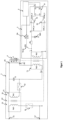
- Figure 1 shows a schematic circuit diagram of a preferred embodiment of a synchronous flyback converter circuit according to the invention.
- the synchronous flyback converter circuit 1 of the Figure 1 comprises a transformer T1 which provides galvanic isolation GT between a primary side PS or input side and a secondary side SS or Output side of the synchronous flyback converter circuit 1. Consequently, the synchronous flyback converter circuit 1 has a galvanic isolation GT between its input E1, E1' and its output A1, A1', which is provided by the transformer T1.
- An electrical energy source or electrical energy supply can be connected to the input, in particular to the at least two input connections E1 and E1' (in Figure 1 not shown), which can provide the synchronous flyback converter circuit 1 in the connected state with a direct voltage or a rectified alternating voltage, which has preferably also been smoothed or filtered, on the input side.
- a lighting system 4 with at least one lighting device 5 can be connected to the output, in particular to the at least two output terminals A1 and A1'.
- the illuminant section 4 comprises three illuminants 5, but according to the invention the illuminant section 4 can also have only one, two or more than three illuminants 5.
- the lighting means 4 can be electrically connected to one another in series and/or in parallel if more than one lighting means is arranged in the lighting means section.
- the lighting means 4 can be any lighting means known to the person skilled in the art whose light emission can be controlled by the electrical energy supplied to the lighting means.
- the lighting means 5 of the lighting means section 4 preferably correspond to a light-emitting diode (LED).
- the lighting means section 4 can comprise any type of LED, such as an organic LED, an inorganic LED, an LED with secondary excitation, etc.
- the lighting means section 4 preferably comprises different types of lighting means or only one type of lighting means.
- the synchronous flyback converter circuit 1 and the illuminant path 4 together form a luminaire according to the invention.
- the input in particular the input terminals E1 and E1'; the primary winding Np1 of the transformer T1; a controllable switch S1; a detection circuit 2 and a control unit 3 are arranged in the synchronous flyback converter circuit 1 shown.
- the primary side switch S1 is electrically connected in series with the primary winding Np1 of the transformer T1.
- the output in particular the output terminals A1 and A1'; the secondary winding Ns1 of the transformer T1; a further controllable switch S2; an optional capacitor C1 and the detection primary winding Np2 of a detection transformer T2 are arranged.
- the detection secondary winding Ns2 of the detection transformer T2 is arranged on the primary side PS, in particular as part of the detection circuit 2.
- the secondary winding Ns1 of the transformer T1 is electrically connected to the optional capacitor C1 and the detection primary winding Np2 of the detection transformer T2 via the further controllable switch S2.
- the lower-potential terminal of the secondary winding Ns1 is electrically connected to the lower-potential terminal of the capacitor C1 and the lower-potential terminal of the detection primary winding Np2 via the further controllable switch S2.
- the further controllable switch S2 can alternatively also be electrically connected to the higher-potential terminal of the secondary winding Ns1.
- the lighting system 4, in particular the lighting system 5, can also be complementary to the Figure 1 shown electrical connection to the output A1, A1'.
- the detection primary winding Np2 of the detection transformer T2 is electrically connected in series to the output, in particular the output terminals A1 and A1'.
- the secondary winding Ns1, the optional capacitor C1 and the series connection of the output of the synchronous flyback converter circuit 1 and the detection primary winding Np2 are electrically connected in parallel to each other.
- the lamp path 4 is connected to the output, in particular to the output terminals A1 and A1', or is electrically connected to it/these, then the lamp path 4 is electrically connected in series with the detection primary winding Np2 of the detection transformer T2. Consequently, the lamp path current i LED flowing through the lamp path 4 also flows through the detection primary winding Np2.
- the detection transformer T2 is arranged such that the detection transformer T2, in particular the core of the detection transformer T2, is operated in saturation or is in saturation when the lamp path current i LED flows through the detection primary winding Np2.
- the optional capacitor C1 is in particular a smoothing capacitor or a filtering capacitor.
- the primary-side controllable switch S1 and the primary winding Np1 of the transformer T1 are set up in such a way that when the controllable switch S1 is in the conductive state, a current flows through the primary winding Np1 of the transformer T1 and the primary-side switch S1 from an electrical energy source that can be connected to the input E1, E1', as a result of which the primary winding Np1 of the transformer T1 is charged with electrical energy.
- the electrical energy is then transferred in a potential-isolated manner from the primary winding Np1 to the secondary winding Ns1, i.e. from the primary side PS to the secondary side SS, when the primary-side controllable switch S1 is switched off.
- the secondary winding Ns1 is then discharged when the primary-side switch S1 is in the non-conductive state.
- the additional controllable switch S2 on the secondary side is preferably clocked complementarily to the controllable switch S1 on the primary side. This means that if the controllable switch S1 on the primary side is switched to be conductive, then the additional controllable switch S2 on the secondary side is not switched to be conductive; and if the controllable switch S1 on the primary side is not switched to be conductive, then the additional controllable switch S2 on the secondary side is switched to be conductive.
- the additional controllable switch S2 on the secondary side is in particular clocked or controlled in such a way that it provides the functionality of a diode for rectification, in particular for half-wave rectification.
- the primary-side switch S1 preferably serves to adjust the electrical energy, current and/or voltage provided at the output of the synchronous flyback converter circuit.
- the clocking of the primary-side controllable switch S1 can convert a DC voltage or rectified voltage supplied on the input side AC voltage can be controlled into an output voltage provided on the output side with a different voltage level.
- the additional switch S2 on the secondary side is preferably used for rectification, in particular half-wave rectification, and the optional capacitor C1 is preferably used for smoothing or filtering.
- the primary-side controllable switch S1, the transformer T1 with the primary winding Np1 and the secondary winding Ns1, the secondary-side further controllable switch S2 and the optional capacitor C1 form a primary clocked voltage converter, namely a synchronous flyback converter.
- the primary-side controllable switch S1 and the secondary-side further controllable switch S2 are preferably a power switch, a field-effect transistor, such as a metal-oxide-semiconductor field-effect transistor (MOSFET), or a bipolar transistor.
- a field-effect transistor such as a metal-oxide-semiconductor field-effect transistor (MOSFET), or a bipolar transistor.
- the primary-side control unit 3 is designed to control the primary-side switch S1 and the secondary-side switch S2 (this is described in the Figure 1 not indicated by corresponding arrows). For this purpose, the primary-side control unit 3 is set up to generate corresponding control signals and to supply these to the primary-side switch S1 and the secondary-side further switch S2. The control of the secondary-side further switch S2 by the primary-side control unit 3 is carried out in particular in a galvanically isolated or potential-separated manner, e.g. via an optocoupler. The primary-side control unit 3 is set up in particular to control the primary-side switch S1 and the secondary-side further switch S2 in accordance with the above statements.
- control unit 3 is designed to adjust the electrical energy, current and/or voltage provided at the output A1, A1' of the synchronous flyback converter circuit 1 and thus to control the operation of the lighting system 4 connected to the output.
- the control unit 3 is in particular designed to control the primary-side switch S1 on the basis of at least one feedback variable, such as on the basis of the lamp path current i LED .
- the detection circuit 2 is designed to generate a to generate a signal S Q which represents the signal and to feed it to the control unit 3.
- control unit 3 can be a processor, a microprocessor, a controller, a microcontroller or an application-specific integrated circuit (ASIC) or a combination of these elements.
- ASIC application-specific integrated circuit
- control unit 3 is a component of the synchronous flyback converter circuit 1.
- control unit 3 can also be an external control unit, ie be arranged outside the synchronous flyback converter circuit 1.
- the detection circuit 2 of the synchronous flyback converter circuit 1 comprises the detection secondary winding Ns2 of the detection transformer T2, a controllable current source StQ, an optional digital-analog converter DA, a measuring unit R1 in the form of a low-resistance measuring resistor, an optional voltage source SpQ, two comparators K1 and K2 and a bistable flip-flop FF.
- the two comparators K1 and K2 and the bistable flip-flop or flip-flop FF form a signal generation unit.
- the current source StQ of the synchronous flyback converter circuit 1 is designed to feed a periodically changing current i c , in particular a triangular current, into the detection secondary winding Ns2 of the detection transformer T2.
- the current source StQ corresponds to a bipolar transistor which can be controlled by the control unit 3 via a digital-analog converter DA.
- the control unit 3 is designed to control the current source StQ of the detection circuit 2 in such a way that it feeds a periodically changing current into the detection secondary winding Ns 2 of the detection transformer T2.
- the current source StQ of the detection circuit 2 can also be implemented in another way according to the invention.
- the detection transformer T2 is arranged in such a way that at the time when the magnetic flux generated at the detection secondary winding Ns2 by the periodically changing current i c exceeds the magnetic flux generated at the detection primary winding Np2 by the lamp path current i LED generated magnetic flux, a detection pulse occurs at the detection secondary winding Ns2.
- the saturation of the detection transformer T2, in particular of the core of the detection transformer T2, caused by the lamp path current i LED is temporarily canceled, so that electrical energy is briefly transferred from the secondary-side detection primary winding Np2 to the primary-side detection secondary winding Ns2, resulting in a detection pulse in the form of a current pulse or current peak at the detection secondary winding Ns2.
- the detection transformer T2 is arranged such that it is operated in saturation by the lamp path current i LED ; and that at the time at which the saturation of the detection transformer T2 is released due to the periodically changing current i c , a detection pulse Imp1, Imp2 is transmitted to the detection secondary winding Ns2.
- the detection transformer T2 comprises a core via which electrical energy can be transferred from the detection primary winding Np2 to the detection secondary winding Ns2 in the unsaturated state of the detection transformer.
- the core of the detection transformer T2 is preferably dimensioned or selected such that the core is operated in saturation by the lamp path current i LED ; and that at the time at which the saturation of the detection transformer T2 is lifted due to the periodically changing current i c , a detection pulse Imp1, Imp2 is transmitted to the detection secondary winding Ns2.
- the measuring unit R1 in the form of a low-resistance measuring resistor or shunt resistor is electrically connected to the detection secondary winding Ns2, in particular to the side of the detection secondary winding Ns2 with the higher potential, so that when a detection pulse occurs on the detection secondary winding Ns2, a corresponding voltage pulse or voltage peak can be measured or tapped on the measuring unit R1.
- the measuring unit R1 can also be implemented in a different way according to the invention.
- the optional voltage source SpQ is electrically connected to the measuring unit R1 and is designed to measure or tap the voltage pulse that can be measured or tapped at the measuring unit R1 and that is caused by the occurrence of a detection pulse at the detection secondary winding Ns2, in particular by superimposing a direct voltage, such that this voltage pulse corresponds to a positive voltage pulse or a voltage pulse with positive polarity, regardless of whether the detection pulse occurs during a rising or falling edge of the periodically changing current i c at the detection secondary winding Ns2.
- the measuring unit R1 which is electrically connected on one side to the detection secondary winding Ns2 of the detection transformer T2, is electrically connected on the other side to the first comparator K1 and second comparator K2, in particular to the positive, non-inverting input of the first comparator K1 and the negative, inverting input of the second comparator K2.
- the first comparator K1 in particular its positive, non-inverting input
- the second comparator K2 in particular its negative, inverting input, are each electrically connected via the measuring unit R1 to the detection secondary winding Ns2 of the detection transformer T2.
- the detection transformer T2 may have, in addition to the detection secondary winding Ns2 (first detection secondary winding), a further primary-side detection secondary winding (second detection secondary winding), which is also coupled to the secondary-side detection primary winding NS1 and is part of the detection circuit (in Figure 1 not shown).
- the measuring unit R1 is preferably electrically connected on one side to the second detection secondary winding and on the other side to the first comparator K1 and second comparator K2, wherein the current source StQ of the synchronous flyback converter circuit 1 is further configured to feed a periodically varying current i c into the first detection secondary winding Ns 2 of the detection transformer T2.
- a detection pulse then preferably occurs at the second detection secondary winding at the time at which the magnetic flux generated at the first detection secondary winding by the periodically changing current i c exceeds the At this time, the saturation of the detection transformer T2, in particular of the core of the detection transformer, caused by the lamp path current i LED is temporarily canceled, so that electrical energy is briefly transferred from the secondary-side detection primary winding Np2 to the second primary-side detection secondary winding, resulting in a detection pulse in the form of a current pulse or current peak at the second detection secondary winding.
- a separation between the periodically changing current, in particular the triangular current, supplied to the detection transformer T 2 on the primary side by the current source StQ and the current peaks or current spikes occurring on the detection transformer on the primary side at the time when the saturation of the detection transformer is removed is not necessary.
- the measuring unit R1 is electrically connected to the second detection secondary winding in the form of a low-resistance measuring resistor or shunt resistor, so that when a detection pulse occurs on the second detection secondary winding, a corresponding voltage pulse or voltage peak can be measured or tapped on the measuring unit R1.
- the measuring unit R1 can also be implemented in a different way according to the invention.
- the optional voltage source SpQ can be electrically connected to the measuring unit R1 and is designed to shift the level of the voltage pulse that can be measured or tapped at the measuring unit R1 and is caused by an occurrence of a detection pulse at the second detection secondary winding, in particular by superimposing a direct voltage, such that this voltage pulse corresponds to a positive voltage pulse or a voltage pulse with positive polarity, regardless of whether the detection pulse occurs during a rising or falling edge of the periodically changing current i c at the second detection secondary winding.
- the first comparator K1 in particular its positive, non-inverting input
- the second comparator K2 in particular its negative, inverting input
- the first comparator K1 is designed to generate a first comparator pulse, in particular a first voltage pulse with positive polarity, at the time of occurrence of the first detection pulse at the detection secondary winding Ns2, wherein the first detection pulse corresponds to a detection pulse that occurs during a rising edge of the periodically changing current i c at the time at which the saturation of the detection transformer T2 is canceled due to the periodically changing current i c .
- a corresponding reference voltage value Uref_p is supplied to the first comparator K1 at its negative, inverting input.
- the second comparator K2 is designed to generate a second comparator pulse, in particular a second voltage pulse with positive polarity, at the time of occurrence of the second detection pulse at the detection secondary winding Ns2, wherein the second detection pulse corresponds to a detection pulse that occurs during a falling edge of the periodically varying current i c at the time at which the saturation of the detection transformer T2 is canceled due to the periodically varying current i c .
- a corresponding reference voltage value Uref_n is supplied to the second comparator K2 at its positive, non-inverting input.
- the comparators K1 and K2 are electrically connected on the output side to the bistable flip-flop FF, whereby the output of the first comparator K1 is connected to the set input S and the output of the second comparator K2 are electrically connected to the reset input R of the bistable flip-flop FF.
- bistable flip-flop FF is designed to generate the signal S Q representing the lamp path current i LED in the form of a square wave signal at its non-inverting output Q. This square wave signal S Q is then fed to the control unit 3.
- the control unit 3 can use the supplied signal S Q digitally or analogously.
- the signal S Q is preferably filtered by a low-pass filter.
- the control unit 3 is preferably designed to determine the lamp path current i LED on the basis of the signal S Q supplied from the detection circuit 2, in particular from the bistable flip-flop FF.
- the control unit 3 is in particular designed to take into account the winding ratio between the detection primary winding Np2 and the detection secondary winding Ns2.
- the duty cycle of the square wave signal S Q output at the non-inverting output Q of the bistable flip-flop FF is a measure of the illuminant path current i LED .
- the detection circuit 2 is designed to evaluate the relative temporal position of at least two detection pulses in a period of the periodically changing current i c as information relating to the lamp path current i LED in order to generate the signal S Q representing the lamp path current i LED .
- the duty cycle of the signal generated by the detection circuit 2, in particular the signal generation unit is dependent on the relative temporal position of the first detection pulse and the second detection pulse in the period of the periodically changing current i c (cf. in this regard Figure 2 ).
- All elements of the detection circuit 2, except for the detection transformer T2 can be components of the control unit 3.
- all Elements of the detection circuit 2, except for the detection transformer T2 are integrated in the control unit 3. (in Figure 1 Not shown)
- Figure 2 shows schematically an example of the temporal course of the periodically changing current as well as of different voltage values of the Figure 1 shown preferred embodiment of a synchronous flyback converter circuit according to the invention.
- the top graph i c (A) / t (s) shows the time course of the periodically changing current i c generated by the current source StQ and fed into the detection secondary winding Ns2.
- the periodically varying current i c corresponds to a triangular current with a corresponding rising edge and falling edge during its period T.
- the current value i S ⁇ T of the periodically varying current i c which is sufficient to cancel the saturation of the detection transformer T2, in particular of the core of the detection transformer T2, caused by the lamp path current i LED , is shown as a horizontal dashed line i S ⁇ T .
- This horizontal dashed line i S ⁇ T therefore indicates the current value of the periodically varying current i c which, according to the turns ratio between the detection primary winding Np2 and the detection secondary winding Ns2, corresponds to the current value of the lamp path current i LED . Therefore, if the winding ratio is 1:1 (number of windings of the detection primary winding Np2 corresponds to the number of windings of the detection secondary winding Ns2), then the current value of the lamp path current i LED is indicated by the horizontal dashed line i S ⁇ T .
- the second graph Us (v) / t (s) shows the time course of the voltage that can be measured or tapped at the measuring unit R1.
- a detection pulse Imp1 or Imp2 is transmitted to the detection secondary winding Ns2 of the detection transformer T2 or a detection pulse Imp1 or Imp2 occurs at the detection secondary winding Ns2, which can be measured or tapped via the measuring unit R1 as a corresponding voltage pulse or voltage peak.
- a detection pulse Imp1 or Imp2 is transmitted to the detection secondary winding Ns2 of the detection transformer T2 or a detection pulse Imp1 or Imp2 occurs at the detection secondary winding Ns2, which can be measured or tapped via the measuring unit R1 as a corresponding voltage pulse or voltage peak.
- the voltage Us has a corresponding voltage pulse caused by a first detection pulse Imp1 with preferably positive polarity (as shown in Figure 2
- the voltage Us has a corresponding voltage pulse caused by a second detection pulse Imp2 with preferably negative polarity (as shown in Figure 2 is indicated).
- both the voltage pulses or voltage peaks caused by a first detection pulse Imp1 and the voltage pulses or voltage peaks caused by a second detection pulse Imp2 are positive because their level has been shifted accordingly by the optional voltage source SpQ. Consequently, the voltage pulses corresponding to the first detection pulses Imp1 have a higher voltage level compared to the voltage pulses corresponding to the second detection pulses Imp2. At times when no voltage pulses or voltage peaks occur (i.e. when the periodically changing current i c does not correspond to the current value i S ⁇ T ), the voltage Us that can be measured at the measuring unit R1 corresponds to the offset voltage provided by the optional voltage source SpQ for level shifting.
- the reference voltage value Uref_p supplied to the negative, inverting input of the first comparator K1 and the reference voltage value Uref_n supplied to the positive, non-inverting input of the second comparator K2 are selected such that the first comparator K1 generates a voltage pulse (first comparator pulse) at the output upon the occurrence of a first detection pulse Imp1 at the detection secondary winding Ns2 and consequently upon occurrence of a corresponding voltage pulse at the measuring unit R1; and that the second comparator K2 generates at the output a voltage pulse (second comparator pulse) upon occurrence of a second detection pulse Imp2 at the detection secondary winding Ns2 and consequently upon occurrence of a corresponding voltage pulse at the measuring unit R1.
- the graph S Q (V) / t(s) shows the time course of the signal S Q representing the lamp path current i LED , which is generated by the detection circuit 2, in particular by the bistable flip-flop FF at its non-inverting output Q.
- the signal S Q changes from a first signal level or voltage level to a second signal level or voltage level when a first comparator pulse occurs. Since the output of the second comparator K2 is electrically connected to the reset input R of the bistable flip-flop FF, the signal S Q changes from the second signal level or voltage level to the first signal level or voltage level when a second comparator pulse occurs.
- the signal generating unit in particular the first comparator K1, the second comparator K2 and the bistable flip-flop FF, is designed to generate, on the basis of the first detection pulse Imp1 and second detection pulse Imp2 transmitted during the period T of the periodically changing current i c , detection pulse Imp2 to generate a signal with two signal levels (i.e. a square wave signal) as signal S Q , wherein at the time of occurrence of the first detection pulse Imp1 the signal S Q changes from a first signal level to a second signal level, and at the time of occurrence of the second detection pulse Imp2 the signal S Q changes from the second signal level to the first signal level.
- two signal levels i.e. a square wave signal
- the duty cycle TG of the signal S Q is a measure of the lamp path current i LED , whereby the following relationship applies: the greater the duty cycle TG of the signal S Q , the lower or smaller the current value of the lamp path current i LED .
- the duty cycle TG of the signal S Q corresponds in particular to the ratio of the pulse duration t2 to the period or period length Ps of the signal S Q .
- the time interval between a first detection pulse Imp1 and a second detection pulse Imp2 in the period T of the periodically changing current i c is lengthened or increased, whereby the time period t2 during which the signal S Q is at the second signal level is lengthened and consequently the duty cycle TG is increased.
- the relative temporal position of at least two detection pulses in particular the relative temporal position of the first detection pulse Imp1 and the second detection pulse Imp2
- a conclusion can be drawn about the lamp path current i LED .
- the time interval between the first detection pulse Imp1 and the second The detection pulse Imp2 in the period T allows a conclusion to be drawn about the lamp path current i LED .
- the winding ratio between the detection primary winding Np2 and the detection secondary winding Ns2 is also taken into account.
- the detection circuit 2 in particular the signal generation unit, is designed to evaluate the relative temporal position of at least two detection pulses in the period of the periodically changing current as information regarding the lamp path current for generating the signal.
- the detection circuit 2 in particular the signal generation unit, is designed to evaluate the time interval between at least two detection pulses in the period of the periodically changing current as information regarding the lamp path current for generating the signal.
- the control unit 3 to which the signal S Q generated by the detection circuit 2 is fed, can then deduce or determine the lamp path current i LED on the basis of this signal S Q , in particular on the basis of the duty cycle TG of this signal S Q . In doing so, the control unit 3 also takes into account in particular the winding ratio between the detection primary winding Np2 and the detection secondary winding Ns2. Consequently, the control unit 3 can use the lamp path current as a feedback variable for controlling the primary-side switch S1.
- Figure 3 shows a schematic circuit diagram of a preferred embodiment of a pulse broadening circuit according to the invention.
- the pulse spreader circuit 6 of the Figure 3 includes an optional diode D1, a capacitor C2, an ohmic resistor R2 and a comparator K3.
- the optional diode D1 is provided to prevent backflow from the capacitor C2 in the charged state to the input E6 of the pulse spreader circuit 6. Consequently, the anode of the diode D1 is electrically connected to the input E6.
- the capacitor C2 and the resistor R2 are electrically connected in parallel to each other, whereby this parallel circuit consists of the capacitor C2 and the Resistor R2 is electrically connected to the positive, non-inverting input of comparator K3 and via the optional diode D1 to input E6 of pulse spreader circuit 6.
- the capacitor C2 is designed in such a way that it is charged by a voltage peak or spike faster than it is discharged again via the resistor R2 after the voltage peak has disappeared.
- the charging time of the capacitor C2 is shorter or faster than the discharging time of the capacitor C2 when discharging via the resistor R2.
- the reference voltage value Uref_ext supplied to the negative, inverting input of the comparator K3 is now selected to be so lower or smaller than the maximum value of the charge of the capacitor C2 that the comparator K3 outputs an output pulse Uout at its output (while the voltage Urc exceeds the reference voltage value Uref_ext) which has a longer pulse duration than the pulse duration of the pulse or voltage peak to be widened originally supplied to the input E6.
- the pulse spreader circuit 6 is designed to convert a pulse supplied via the input E6, such as the above-mentioned detection pulse transmitted to the detection secondary winding Ns2 of the detection transformer T2, in particular the first detection pulse and/or the second detection pulse, into a corresponding output pulse Uout provided at the output A6, the pulse duration of which is longer or greater than the pulse duration of the original pulse supplied at the input E6.
- the synchronous flyback converter circuit 1, in particular the detection circuit 2, of the Figure 1 preferably has at least one pulse spreader circuit 6 according to the Figure 3 on, whereby these at least one detection circuit is preferably arranged between the measuring unit R1 and the two comparators K1 and K2 (in Figure 1 Not shown).
- the at least one pulse widening circuit 6 is designed to widen the voltage pulse measurable at the measuring unit R1, in particular to extend its pulse duration, when a detection pulse, in particular a first detection pulse or a second detection pulse, is transmitted to the detection secondary winding Ns2.
- a detection pulse in particular a first detection pulse or a second detection pulse
- the voltage pulse supplied to the first comparator K1 and second comparator K2 which corresponds to a first detection pulse Imp1 occurring at the detection secondary winding Ns2, having an extended pulse duration
- the voltage pulse supplied to the first comparator K1 and second comparator K2 which corresponds to a second detection pulse Imp2 occurring at the detection secondary winding Ns2, having an extended pulse duration.
- the output of the first comparator K1 can be fed via a pulse spreader circuit 6 according to the Figure 3 with the set input S of the bistable flip-flop FF and the output of the second comparator K2 via a further pulse spreader circuit 6 according to the Figure 3 be electrically connected to the reset input R of the bistable flip-flop FF.
- the voltage pulses output in this case by the comparators K1 and K2 of the detection circuit 2 and the voltage pulses extended in time by the respective pulse spreader circuit 6 fed to the set input S and reset input R of the bistable flip-flop FF are in the Figure 4b shown schematically.
- Figure 4A shows schematically an example of the broadening of impulses by the Figure 3 shown preferred embodiment of a pulse broadening circuit according to the invention.
- the voltage Ure has a falling discharge edge following the rising charging edge.
- the steepness of the rising charging edge is steeper or greater than the steepness of the falling discharging edge, since the discharging process of the capacitor C2 via the resistor R2 is slower, in particular significantly slower, than the preceding charging process of the capacitor C2.
- the reference voltage value Uref_ext supplied to the negative, inverting input of the comparator K3 is now selected to be smaller than the maximum value of the charge of the capacitor C2 in such a way that the voltage Urc supplied to the positive, non-inverting input is greater than the reference voltage value Uref_ext during a time period which is longer or greater than the time period of the voltage pulse of the input voltage Uin of the pulse spreader circuit 6.
- the comparator K3 outputs a pulse that has a longer pulse duration compared to the corresponding pulse that was supplied on the input side.
- Figure 4B shows schematically an example of the broadening of pulses when in the Figure 1
- the first and second comparators are each electrically connected to the bistable flip-flop via a pulse broadening circuit according to the invention.
- time course of the voltage Uset ⁇ corresponds to the time course of the voltage signal output by the first comparator K1 and the time course of the voltage Ureset' corresponds to the time course of the voltage signal output by the second comparator K2.
- the temporal course of the voltage Uset corresponds to the temporal course of the voltage signal Uset' after the voltage pulses of the voltage signal Uset' have been propagated by the respective pulse spreader circuit according to the invention were widened, whereby this voltage signal Uset is fed to the set input S of the bistable flip-flop FF.
- the temporal course of the voltage Ureset corresponds to the temporal course of the voltage signal Ureset' after the voltage pulses of the voltage signal Ureset' have been widened by the respective pulse widening circuit according to the invention, wherein this voltage signal Ureset is fed to the reset input R of the bistable flip-flop FF.
- the time course of the voltage S Q corresponds to the time course of the voltage signal that is generated by the non-inverting output Q of the bistable flip-flop FF.
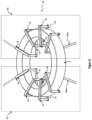
- Figure 5A shows schematically a preferred embodiment of an arrangement of the detection transformer of the synchronous flyback converter circuit according to the invention with respect to a circuit board.
- the Figure 5A shows in particular a schematic plan view (upper view of the Figure 5A ) and a cross-section (lower illustration of the Figure 5A ) a preferred embodiment of an arrangement of the detection transformer of the synchronous flyback converter circuit according to the invention with respect to a circuit board.
- FIG. 5A a section of a printed circuit board LP is shown on which the synchronous flyback converter circuit according to the invention is arranged.
- Figure 5A shows schematically the arrangement of the detection transformer T2 whose primary winding Np2 is arranged on the secondary side SS and whose secondary winding Ns2 is arranged on the primary side PS of the synchronous flyback converter circuit.
- the detection transformer T2 of the Figure 5A comprises a core 7, in particular a toroidal core, via which electrical energy can be transmitted in a potential-separated manner from the detection primary winding NP2 to the detection secondary winding Ns2.
- the core 7 of the detection transformer T2 is in particular dimensioned such that the detection transformer T2, in particular the core 7, is operated in saturation or is in saturation when a lamp path current flows through the secondary-side detection primary winding Np2.
- the core 7 as well as part of the windings of the detection primary winding Np2 and the detection secondary winding Ns2 are inserted into a recess or cavity of the printed circuit board LP.
- the windings are then closed by closing the windings using short-circuit bridges 8 during production after the core 7 and the part of the windings, in particular the lower part of the windings, have been inserted into the recess of the printed circuit board LP.
- the core 7 is enclosed by the part of the windings already inserted in the cavity (lower part of the windings) and the short-circuit bridges 8, so that the detection primary winding Np2 and detection secondary winding are then formed on the core 7.
- a short-circuit bridge is also referred to as a jumper and corresponds in particular to a bridging line that is placed on the windings from above in order to close the windings in the area of the bridging line. Consequently, the part of the windings already arranged in the recess of the printed circuit board LP can be closed using a short-circuit bridge in order to produce windings of the detection primary winding Np2 and/or the detection secondary winding Ns2.
- the windings of the detection transformer T2 are formed such that at the bottom of the recess of the printed circuit board LP the windings of the detection primary winding Np2 and/or the detection secondary winding Ns2 are formed by a corresponding conductive layer; and that the windings on the opposite side are formed by one or more short-circuit bridges 8.
- the windings are formed by a corresponding conductive layer; and on the opposite side of the core 7, i.e. above the core, the windings are then closed or formed by one or more short-circuit bridges 8.
- the conductive layer may preferably be an inner layer or the bottom or outermost layer of the circuit board if the circuit board comprises several conductive layers.
- Three short-circuit bridges 8 are provided to generate the windings of the detection primary winding Np2 and To generate the windings of the detection secondary winding Ns2, five short-circuit bridges 8 are provided. Consequently, in the Figure 5A shown detection transformer T2, the number of windings of the detection secondary winding Ns2 is greater than the number of windings of the detection primary winding Np2. The number of windings of the detection secondary winding Ns2 and the number of windings of the detection primary winding Np2 can also be added to the number shown in Figure 5A The number shown may vary.
- the winding ratio between the detection primary winding Np2 and the detection secondary winding Ns2 can be easily adjusted.
- the short-circuit bridges can be easily mounted preferably by plugging them into corresponding holes 10 of the printed circuit board LP.
- Figure 5B shows schematically a further preferred embodiment of an arrangement of the detection transformer of the synchronous flyback converter circuit according to the invention with respect to a circuit board.
- the Figure 5B shows in particular a schematic plan view (upper view of the Figure 5B ) and a cross-section (lower illustration of the Figure 5B ) a preferred embodiment of an arrangement of the detection transformer of the synchronous flyback converter circuit according to the invention with respect to a circuit board.
- the detection transformer T2 and consequently the core 7 and the windings of the detection primary winding Np2 and the detection secondary winding Ns2 are fully integrated in the printed circuit board.
- the windings of the detection transformer T2 are formed in particular in such a way that at the bottom of the recess of the circuit board the windings of the detection primary winding Np2 and/or the detection secondary winding Ns2 are formed by a corresponding conductive layer; and that the windings on the opposite side are formed by one or more conductor tracks 9.
- the windings are formed by a corresponding conductive layer; and on the opposite side of the core 7, i.e. above the core, the windings are then closed or formed by one or more conductor tracks 9.
- the conductive layer may preferably be an inner layer or the bottom or outermost layer of the circuit board if the circuit board comprises several conductive layers.
- the number of windings of the detection secondary winding Ns2 is greater than the number of windings of the detection primary winding Np2.
- the number of windings of the detection secondary winding Ns2 and the number of windings of the detection primary winding Np2 can also be added to the number shown in Figure 5B The number shown may vary.
- the winding ratio between the detection primary winding Np2 and the detection secondary winding Ns2 can therefore be easily adjusted using conductor tracks 9.
- Figure 6 shows a schematic side view of a preferred embodiment of the detection transformer of the synchronous flyback converter circuit according to the invention.
- the formation of windings of the detection primary winding Np2 and the detection secondary winding Ns2 of the Figure 6 The detection transformer T2 shown in Figure 1 is determined by the Figure 5A described principle, ie by using short-circuit bridges 8 or jumpers.
- the core 7 of the detection transformer T2 is in particular dimensioned such that the detection transformer T2, in particular the core 7, is operated in saturation or is in saturation when a lamp path current flows through the secondary-side detection primary winding Np2.
- the core 7 and a part 11 of the windings of the detection primary winding Np2 and the detection secondary winding Ns2 are inserted into a recess or cavity of a printed circuit board (printed circuit board is in Figure 6 not shown).
- the windings are then closed by closing the windings by short-circuit bridges 8 during production after the core 7 and the part 11 of the windings, in particular the lower part 11 of the windings, have been inserted into the recess of the circuit board.
- the core 7 is enclosed by the part 11 of the windings already inserted in the cavity (lower part of the windings) and the short-circuit bridges 8 (upper part of the windings), so that the detection primary winding Np2 and detection secondary winding are then formed on the core 7.
- a short-circuit bridge 8 is also called a jumper and corresponds in particular to a bridging line that is placed from above on the already existing part 11 of the windings in order to close the windings in the area of the bridging line. Consequently, the part 11 of the windings already arranged in the recess of the printed circuit board can be closed by a short-circuit bridge 8 in order to create windings of the detection primary winding Np2 and/or the detection secondary winding Ns2.
- the windings of the detection transformer T2 are formed such that at the bottom of the recess of the printed circuit board the windings of the detection primary winding Np2 and/or the detection secondary winding Ns2 are formed by a corresponding conductive layer 11; and that the windings on the opposite side are formed by one or more short-circuit bridges 8.
- the windings are formed by a corresponding conductive layer 11 is formed; and on the opposite side of the core 7, ie above the core, the windings are then closed or formed by one or more short-circuit bridges 8.
- the conductive layer may preferably be an inner layer or the bottom or outermost layer of the circuit board if the circuit board comprises several conductive layers.
- the number of windings of the detection secondary winding Ns2 is equal to the number of windings of the detection primary winding Np2.
- the number of windings of the detection secondary winding Ns2 and the number of windings of the detection primary winding Np2 can also be added to the number shown in Figure 6 The number shown may vary.
- the winding ratio between the detection primary winding Np2 and the detection secondary winding Ns2 can be easily adjusted.
- the methods described above for forming or generating the detection primary winding Np2 and the detection secondary winding Ns2 of the detection transformer T2 can preferably also be used for forming or generating the primary winding Np1 and secondary winding Ns1 of the transformer T1 of the synchronous flyback converter circuit according to the invention.
Landscapes
- Dc-Dc Converters (AREA)
- Circuit Arrangement For Electric Light Sources In General (AREA)
Claims (15)
- Circuit de convertisseur à récupération synchrone (1) destiné à faire fonctionner une section de moyens d'éclairage (4) comportant au moins un moyen d'éclairage (5), en particulier comportant au moins une diode électroluminescente, le circuit de convertisseur à récupération synchrone (1) comprenant :- un transformateur (T1) comportant un enroulement primaire (Np1), qui est connecté électriquement à un interrupteur commandable (S1), et un enroulement secondaire (Ns1), auquel la section de moyens d'éclairage (4) peut être connectée par l'intermédiaire d'une sortie (A1, A1') du circuit de convertisseur à récupération synchrone (1), et- un circuit de détection (2) pour la génération d'un signal (SQ) qui reflète le courant de la section de moyens d'éclairage (iLED) qui circule à travers la section de moyens d'éclairage (4) lorsque la section de moyens d'éclairage (4) est connectée à l'enroulement secondaire (Ns1) ;- le transformateur (T1) séparant galvaniquement un côté primaire (PS) du circuit de convertisseur à récupération synchrone (1) et un côté secondaire (SS) du circuit de convertisseur à récupération synchrone (1) ;- l'enroulement primaire (Np1), l'interrupteur commandable (S1), et le circuit de détection (2) étant disposés sur le côté primaire (PS) et l'enroulement secondaire (Ns1) et la sortie (A1, A1') étant disposés sur le côté secondaire (SS) ;- le circuit de détection (2) comprenant :- un transformateur de détection (T2) comportant un côté primaire comportant un enroulement primaire de détection (Np2) et un côté secondaire comportant un enroulement secondaire de détection (Ns2),l'enroulement primaire de détection (Np2) sur le côté secondaire du transformateur (T1) du circuit de convertisseur à récupération synchrone et étant connecté électriquement en série avec la sortie du circuit de convertisseur à récupération synchrone (A1, A1'), etle transformateur de détection (T2) étant conçu de telle sorte que le transformateur de détection (T2) est actionné à saturation par le courant de la section de moyen d'éclairage (iLED) ;- une source de courant (StQ) conçue pour l'alimentation d'un courant (ic) variant périodiquement à l'enroulement secondaire de détection (Ns2) ; et- une unité de génération de signal (K1, K2, FF) pour la génération du signal ;- le transformateur de détection (T2) étant conçu de telle sorte qu'au moment où la saturation du transformateur de détection (T2) est supprimée en raison du courant (ic) variant périodiquement, une impulsion de détection (Imp1, Imp2) est transmise à l'enroulement secondaire de détection (Ns2) ;- l'unité de génération de signal (K1, K2, FF) étant conçue pour évaluer la position temporelle relative d'au moins deux impulsions de détection (Imp1, Imp2) dans une période du courant (ic) variant périodiquement, en tant qu'information concernant le courant de la section de moyens d'éclairage (iLED) pour la génération du signal (SQ).
- Circuit de convertisseur à récupération synchrone (1) selon la revendication 1,- la source de courant (StQ) étant conçue pour l'alimentation d'un courant (ic) variant périodiquement ayant un front montant et un front descendant pendant la période à l'enroulement secondaire de détection (Ns2) ; et- le transformateur de détection (T2) étant conçu de telle sorte,- que, pendant un front montant, une première impulsion de détection (Imp1) est transmise à l'enroulement secondaire de détection (Ns2) au moment où la saturation du transformateur de détection (T2) est supprimée en raison du courant (ic) variant périodiquement, et- que, pendant un front descendant, une seconde impulsion de détection (Imp2) est transmise à l'enroulement secondaire de détection (Ns2) au moment où la saturation du transformateur de détection (T2) est supprimée en raison du courant (ic) variant périodiquement,- de préférence, la première impulsion de détection (Imp1) et la seconde impulsion de détection (Imp2) différant en termes de leur polarité.
- Circuit de convertisseur à récupération synchrone (1) selon la revendication 2,- l'unité de génération de signal (K1, K2, FF) étant conçue pour générer, sur la base de la première impulsion de détection (Imp1) et de la seconde impulsion de détection (Imp2) transmises pendant la période du courant variant périodiquement, en tant que signal (SQ), un signal ayant deux niveaux de signal,- au moment de l'apparition de la première impulsion de détection (Imp1), le signal passant d'un premier niveau de signal à un second niveau de signal, et- au moment de l'apparition de la seconde impulsion de détection (Imp2), le signal passant du second niveau de signal au premier niveau de signal,- de préférence, le rapport cyclique du signal (SQ) généré par l'unité de génération de signal (K1, K2, FF) étant une mesure du courant de section de moyens d'éclairage (iLED),- de préférence encore, plus le rapport cyclique du signal (SQ) généré par l'unité de génération de signal (K1, K2, FF) est grand, plus le courant de section de moyens d'éclairage (iLED) est faible.
- Circuit de convertisseur à récupération synchrone (1) selon l'une des revendications 2 ou 3,- le circuit de détection (2) étant conçu pour modifier le niveau de la première impulsion de détection (Imp1) et de la seconde impulsion de détection (Imp2) transmises pendant la période du courant (ic) variant périodiquement de telle sorte que la première impulsion de détection (Imp1) et la seconde impulsion de détection (Imp2) transmises pendant la période du courant (ic) variant périodiquement sont converties en impulsions de tension positives, le niveau de l'impulsion de tension correspondant à la première impulsion de détection (Imp1) étant supérieur au niveau de l'impulsion de tension correspondant à la seconde impulsion de détection (Imp2).
- Circuit de convertisseur à récupération synchrone (1) selon l'une des revendications 2 à 4,- l'unité de génération de signal (K1, K2, FF) présentant deux comparateurs (K1, K2) qui sont connectés électriquement à l'enroulement secondaire de détection (Ns2),- un premier comparateur (K1) des deux comparateurs (K1, K2) étant conçu pour la génération d'une première impulsion de comparateur au moment de l'apparition de la première impulsion de détection (Imp1) sur l'enroulement secondaire de détection (Ns2), et- un deuxième comparateur (K2) des deux comparateurs (K1, K2) étant conçu pour la génération d'une deuxième impulsion de comparateur au moment de l'apparition de la seconde impulsion de détection (Imp2) sur l'enroulement secondaire de détection (Ns2),
de préférence :- l'unité de génération de signal (K1, K2, FF) présentant une bascule bistable (FF) qui est connectée électriquement aux deux comparateurs (K1, K2) ;- le premier comparateur (K1) étant connecté électriquement à une entrée d'établissement (S) de la bascule bistable (FF) et le deuxième comparateur (K2) étant connecté électriquement à une entrée de remise à zéro (R) de la bascule bistable (FF) ; et- la sortie non négative (Q) de la bascule bistable (FF) étant prévue pour la délivrance du signal (SQ). - Circuit de convertisseur à récupération synchrone (1) selon l'une des revendications précédentes,- le circuit de convertisseur à récupération synchrone (1) présentant une unité de commande (3) disposée sur le côté primaire (PS) du circuit de convertisseur à récupération synchrone (1) pour la synchronisation du commutateur commandable (S1) et la commande de la source de courant (StQ),- l'unité de commande (1) commandant la source de courant (StQ) de telle sorte que la fréquence du courant (ic) variant périodiquement est supérieure à la fréquence de synchronisation du commutateur commandable (S1).
- Circuit de convertisseur à récupération synchrone (1) selon l'une des revendications précédentes,- le courant (ic) variant périodiquement étant un courant triangulaire.
- Circuit de convertisseur à récupération synchrone (1) selon l'une des revendications précédentes,- la source de courant (StQ) présentant au moins un transistor bipolaire pour délivrer le courant (ic) variant périodiquement.
- Circuit de convertisseur à récupération synchrone (1) selon l'une des revendications précédentes,- le circuit de convertisseur à récupération synchrone (1) présentant au moins un circuit d'élargissement d'impulsion (6) comportant un circuit parallèle d'un condensateur (C2) et d'une résistance ohmique (R2) et comportant un troisième comparateur (K3),- le condensateur (C2) et la résistance ohmique (R2) étant conçus de telle sorte que le condensateur (C2) est chargé par une impulsion (Uin) appliquée au circuit d'élargissement d'impulsion (6) pendant la durée de l'impulsion (Uin), pour être ensuite déchargé à nouveau par l'intermédiaire de la résistance ohmique (R2), le processus de décharge étant plus long que le processus de charge,- le troisième comparateur (K3) étant conçu pour comparer la tension (Urc) chutant aux bornes du circuit parallèle à une valeur de tension de référence (ref_ext) qui est choisie inférieure à la valeur maximale de la charge du condensateur (C2) de telle sorte que l'impulsion de sortie (Uout) délivrée par le troisième comparateur (K3), tandis que la tension (Urc) aux bornes du circuit parallèle dépasse la valeur de tension de référence (ref_ext), est élargie par rapport à l'impulsion (Uin) fournie,- de préférence, plus la valeur de tension de référence (ref_ext) est choisie basse, plus l'impulsion de sortie (Uout) est large par comparaison avec l'impulsion (Uin) fournie.
- Circuit convertisseur à récupération synchrone (1) selon la revendication 9, en référence à la revendication 5,- le premier comparateur (K1) et/ou le deuxième comparateur (K2) étant connecté électriquement à l'enroulement secondaire de détection (Ns2) par l'intermédiaire du circuit d'élargissement d'impulsion (6) ; et/ou- le premier comparateur (K1) et/ou le deuxième comparateur (K2) étant connecté électriquement à la bascule bistable (FF) par l'intermédiaire du circuit d'élargissement d'impulsion (6).
- Circuit de convertisseur à récupération synchrone (1) selon l'une quelconque des revendications précédentes, dans lequel- le circuit de convertisseur à récupération synchrone est disposé sur une carte de circuit imprimé ;- le transformateur de détection (T2) présentant un noyau (7), en particulier un noyau annulaire, pour la transmission d'énergie électrique à partir de l'enroulement primaire de détection (Np2) vers l'enroulement secondaire de détection (Ns2), et- le noyau (7) ainsi qu'une partie des enroulements de l'enroulement primaire de détection (Np2) et de l'enroulement secondaire de détection (Ns2) sont insérés dans un renfoncement de la carte de circuit imprimé,
de préférence :- au moins un pont de court-circuit (8) étant disposé sur l'enroulement primaire de détection (Np2) et/ou l'enroulement secondaire de détection (Ns2), et- le rapport d'enroulement entre l'enroulement primaire de détection (Np2) et l'enroulement secondaire de détection (Ns2) pouvant être réglé par l'au moins un pont de court-circuit (8). - Circuit de convertisseur à récupération synchrone (1) selon la revendication 11, dans lequel- l'au moins un pont de court-circuit (8) est conçu pour fermer la partie des enroulements de l'enroulement primaire de détection (Np2) et/ou de l'enroulement secondaire de détection (Ns2) disposée dans le renfoncement de la carte de circuit imprimé, ce qui permet d'augmenter de manière correspondante le nombre d'enroulements de l'enroulement primaire de détection (Np2) et/ou de l'enroulement secondaire de détection (Ns2).
- Circuit de convertisseur à récupération synchrone (1) selon la revendication 11, dans lequel- le noyau (7) du transformateur de détection est entièrement intégré dans la carte de circuit imprimé, et- au moins une piste conductrice (9) est disposée sur l'enroulement primaire de détection (Np2) et/ou l'enroulement secondaire de détection (Ns2),- et le rapport d'enroulement entre l'enroulement primaire de détection (Np2) et l'enroulement secondaire de détection (Ns2) est de préférence réglable par l'au moins une piste conductrice (9),- de préférence, l'au moins une piste conductrice (9) étant conçue pour fermer des enroulements de l'enroulement primaire de détection (Np2) et/ou de l'enroulement secondaire de détection (Ns2), ce qui permet d'augmenter de manière correspondante le nombre d'enroulements de l'enroulement primaire de détection (Np2) ou de l'enroulement secondaire de détection (Ns2).
- Luminaire, comportant- un circuit de convertisseur à récupération synchrone (1) selon l'une quelconque des revendications précédentes, et- une section de moyens d'éclairage (4) comprenant au moins un moyen d'éclairage (5), en particulier comprenant au moins une diode électroluminescente ;- le circuit de convertisseur à récupération synchrone (1) étant conçu pour fournir côté sortie, à partir d'une tension d'entrée fournie côté entrée, une tension de sortie pour faire fonctionner la section de moyens d'éclairage (4).
- Procédé pour la détection du courant de section de moyens d'éclairage (iLED) dans un circuit de conversion à récupération synchrone (1) selon l'une des revendications 1 à 13, lorsque la section de moyens d'éclairage (4) est connectée à l'enroulement secondaire (Ns1) du transformateur (T1) du circuit de conversion à récupération synchrone (1), le procédé comprenant les étapes suivantes :- alimentation, avec la source de courant (StQ), d'un courant (ic) variant périodiquement dans l'enroulement secondaire de détection (Ns2) ;- transmission, avec le transformateur de détection (T2), d'une impulsion de détection (Imp1, Imp2) à l'enroulement secondaire de détection (Ns2) au moment où la saturation du transformateur de détection (T2) est supprimée en raison du courant (ic) variant périodiquement ; et- évaluation, avec l'unité de génération de signal (2), de la position temporelle relative d'au moins deux impulsions de détection (Imp1, Imp2) dans une période du courant (ic) variant périodiquement, en tant qu'information concernant le courant de section de moyens d'éclairage (iLED) pour la génération du signal (SQ).
Applications Claiming Priority (2)
| Application Number | Priority Date | Filing Date | Title |
|---|---|---|---|
| DE102018119017.4A DE102018119017A1 (de) | 2018-08-06 | 2018-08-06 | Synchrone Sperrwandlerschaltung zum Betrieb einer Leuchtmittelstrecke |
| PCT/EP2019/069307 WO2020030394A1 (fr) | 2018-08-06 | 2019-07-17 | Circuit convertisseur à transfert indirect synchrone pour faire fonctionner une section de moyen d'éclairage |
Publications (2)
| Publication Number | Publication Date |
|---|---|
| EP3815469A1 EP3815469A1 (fr) | 2021-05-05 |
| EP3815469B1 true EP3815469B1 (fr) | 2024-06-19 |
Family
ID=67514604
Family Applications (1)
| Application Number | Title | Priority Date | Filing Date |
|---|---|---|---|
| EP19748759.8A Active EP3815469B1 (fr) | 2018-08-06 | 2019-07-17 | Convertisseur indirect synchrone pour le fonctionnement d'un moyen d'éclairage |
Country Status (4)
| Country | Link |
|---|---|
| EP (1) | EP3815469B1 (fr) |
| AT (1) | AT17779U1 (fr) |
| DE (1) | DE102018119017A1 (fr) |
| WO (1) | WO2020030394A1 (fr) |
Citations (3)
| Publication number | Priority date | Publication date | Assignee | Title |
|---|---|---|---|---|
| GB1488262A (en) * | 1975-04-03 | 1977-10-12 | Ti Ltd | Measuring direct current |
| US20110037414A1 (en) * | 2009-08-14 | 2011-02-17 | Nanjing University Of Aeronautics And Astronautics | Driving apparatus for light emitting diodes |
| US20160033555A1 (en) * | 2014-07-31 | 2016-02-04 | Vacuumschmelze Gmbh & Co. Kg | Flux-gate current sensor with additional frequency measuring |
Family Cites Families (6)
| Publication number | Priority date | Publication date | Assignee | Title |
|---|---|---|---|---|
| JPH07128373A (ja) * | 1993-11-02 | 1995-05-19 | Sumitomo Special Metals Co Ltd | 直流電流センサー |
| ATE503367T1 (de) * | 2008-04-03 | 2011-04-15 | Sander Elektronik Ag | Schaltung und verfahren zur speisung einer led- leuchte |
| DE102009010260A1 (de) * | 2009-02-24 | 2010-09-02 | Osram Gesellschaft mit beschränkter Haftung | Schaltungsanordnung und Verfahren zum Betreiben einer Beleuchtungseinrichtung |
| DE202010013046U1 (de) * | 2010-12-02 | 2011-04-14 | Loewe Opta Gmbh | Transformator |
| JP5606941B2 (ja) * | 2011-01-26 | 2014-10-15 | ヒロセ電機株式会社 | フラックスゲートセンサ |
| DE102016010615B4 (de) * | 2016-09-01 | 2018-10-11 | Diehl Aerospace Gmbh | Sperrwandler mit Betriebsverfahren, Leuchte und Flugzeug |
-
2018
- 2018-08-06 DE DE102018119017.4A patent/DE102018119017A1/de not_active Withdrawn
- 2018-12-04 AT ATGM50217/2018U patent/AT17779U1/de not_active IP Right Cessation
-
2019
- 2019-07-17 EP EP19748759.8A patent/EP3815469B1/fr active Active
- 2019-07-17 WO PCT/EP2019/069307 patent/WO2020030394A1/fr not_active Ceased
Patent Citations (3)
| Publication number | Priority date | Publication date | Assignee | Title |
|---|---|---|---|---|
| GB1488262A (en) * | 1975-04-03 | 1977-10-12 | Ti Ltd | Measuring direct current |
| US20110037414A1 (en) * | 2009-08-14 | 2011-02-17 | Nanjing University Of Aeronautics And Astronautics | Driving apparatus for light emitting diodes |
| US20160033555A1 (en) * | 2014-07-31 | 2016-02-04 | Vacuumschmelze Gmbh & Co. Kg | Flux-gate current sensor with additional frequency measuring |
Also Published As
| Publication number | Publication date |
|---|---|
| EP3815469A1 (fr) | 2021-05-05 |
| DE102018119017A1 (de) | 2020-02-06 |
| AT17779U1 (de) | 2023-02-15 |
| WO2020030394A1 (fr) | 2020-02-13 |
Similar Documents
| Publication | Publication Date | Title |
|---|---|---|
| AT517708B1 (de) | Schaltung zum betreiben mindestens einer led | |
| DE102016124523B4 (de) | Steuerverfahren und -vorrichtung mit Primärseitenregelung in einem quasiresonanten Wechselstrom/Gleichstrom-Sperrwandler ohne analogen Teiler und Leitungserfassung | |
| DE102013224749B4 (de) | Treiberschaltung für Leuchtmittel, insbesondere LEDs, LED-Modul und Leuchte, jeweils mit einer solchen Schaltung, sowie entsprechendes Verfahren | |
| DE102014102276A1 (de) | LED-Netzteil | |
| DE102010037684A1 (de) | LED-Treiber mit Abblendsteuerung mit offfenem Regelkreis | |
| EP3114898B1 (fr) | Led-driver | |
| EP2891382B1 (fr) | Appareil de commande permettant de commander une ligne de del | |
| DE102016102160A1 (de) | Steuermodul mit einer Einrichtung zum Schätzen einer Elektrischen Grösse für einen Schaltwandler und Verfahren zum Steuern eines Schaltwandlers | |
| DE102013219153B4 (de) | Treibermodul mit sekundärseitiger Erkennung einer primärseitigen elektrischen Versorgung | |
| DE102017131163A1 (de) | Llc-leistungswandler und dessen schaltverfahren | |
| EP3284319B1 (fr) | Convertisseur de moyen d'éclairage | |
| DE102014214744A1 (de) | Aktive Schaltung zur Erfassung eines Leuchtmittel-Stroms | |
| DE10030176A1 (de) | Entladungslampen-Lichtstromkreis | |
| WO2016087206A1 (fr) | Circuit convertisseur à temps mort adaptatif | |
| DE102008064399A1 (de) | Verfahren und Betriebsgerät zum Betreiben eines Leuchtmittels mit geregeltem Strom | |
| EP3815469B1 (fr) | Convertisseur indirect synchrone pour le fonctionnement d'un moyen d'éclairage | |
| EP3487055B1 (fr) | Alimentation en tension auxiliaire | |
| DE102004033125A1 (de) | Vorrichtung zur Ansteuerung von Leistungstransistoren | |
| DE112022005681T5 (de) | Controller für einen Sperrumsetzer | |
| EP2478629B1 (fr) | Ballast pour moyens d'éclairage | |
| DE102015206982B4 (de) | Leuchtmittelkonverter mit symmetrierten Ausgangsströmen sowie Verfahren zum Symmetrieren | |
| EP3439159B1 (fr) | Réduction de fluctuations de flux lumineux dans une commande de valeur seuil d'un convertisseur cadencé activement | |
| DE102014107429A1 (de) | Schaltungsvorrichtung und Verfahren zum Betreiben der Schaltungsvorrichtung | |
| EP2208402B1 (fr) | Ballast pour lampe à décharge, par exemple pour une lampe dhi | |
| EP3231253A1 (fr) | Circuit d'attaque à commande de démarrage llc |
Legal Events
| Date | Code | Title | Description |
|---|---|---|---|
| STAA | Information on the status of an ep patent application or granted ep patent |
Free format text: STATUS: UNKNOWN |
|
| STAA | Information on the status of an ep patent application or granted ep patent |
Free format text: STATUS: THE INTERNATIONAL PUBLICATION HAS BEEN MADE |
|
| PUAI | Public reference made under article 153(3) epc to a published international application that has entered the european phase |
Free format text: ORIGINAL CODE: 0009012 |
|
| STAA | Information on the status of an ep patent application or granted ep patent |
Free format text: STATUS: REQUEST FOR EXAMINATION WAS MADE |
|
| 17P | Request for examination filed |
Effective date: 20210201 |
|
| AK | Designated contracting states |
Kind code of ref document: A1 Designated state(s): AL AT BE BG CH CY CZ DE DK EE ES FI FR GB GR HR HU IE IS IT LI LT LU LV MC MK MT NL NO PL PT RO RS SE SI SK SM TR |
|
| STAA | Information on the status of an ep patent application or granted ep patent |
Free format text: STATUS: EXAMINATION IS IN PROGRESS |
|
| 17Q | First examination report despatched |
Effective date: 20210625 |
|
| DAV | Request for validation of the european patent (deleted) | ||
| DAX | Request for extension of the european patent (deleted) | ||
| REG | Reference to a national code |
Ref country code: DE Free format text: PREVIOUS MAIN CLASS: H05B0033080000 Ipc: H05B0045000000 Ref legal event code: R079 Ref document number: 502019011486 Country of ref document: DE |
|
| GRAP | Despatch of communication of intention to grant a patent |
Free format text: ORIGINAL CODE: EPIDOSNIGR1 |
|
| STAA | Information on the status of an ep patent application or granted ep patent |
Free format text: STATUS: GRANT OF PATENT IS INTENDED |
|
| RIC1 | Information provided on ipc code assigned before grant |
Ipc: H05B 45/00 20200101AFI20240103BHEP |
|
| INTG | Intention to grant announced |
Effective date: 20240131 |
|
| RAP3 | Party data changed (applicant data changed or rights of an application transferred) |
Owner name: TRIDONIC GMBH & CO KG |
|
| GRAS | Grant fee paid |
Free format text: ORIGINAL CODE: EPIDOSNIGR3 |
|
| GRAA | (expected) grant |
Free format text: ORIGINAL CODE: 0009210 |
|
| STAA | Information on the status of an ep patent application or granted ep patent |
Free format text: STATUS: THE PATENT HAS BEEN GRANTED |
|
| P01 | Opt-out of the competence of the unified patent court (upc) registered |
Effective date: 20240502 |
|
| AK | Designated contracting states |
Kind code of ref document: B1 Designated state(s): AL AT BE BG CH CY CZ DE DK EE ES FI FR GB GR HR HU IE IS IT LI LT LU LV MC MK MT NL NO PL PT RO RS SE SI SK SM TR |
|
| REG | Reference to a national code |
Ref country code: GB Ref legal event code: FG4D Free format text: NOT ENGLISH |
|
| REG | Reference to a national code |
Ref country code: CH Ref legal event code: EP |
|
| REG | Reference to a national code |
Ref country code: DE Ref legal event code: R096 Ref document number: 502019011486 Country of ref document: DE |
|
| REG | Reference to a national code |
Ref country code: DE Ref legal event code: R084 Ref document number: 502019011486 Country of ref document: DE |
|
| PG25 | Lapsed in a contracting state [announced via postgrant information from national office to epo] |
Ref country code: BG Free format text: LAPSE BECAUSE OF FAILURE TO SUBMIT A TRANSLATION OF THE DESCRIPTION OR TO PAY THE FEE WITHIN THE PRESCRIBED TIME-LIMIT Effective date: 20240619 |
|
| PG25 | Lapsed in a contracting state [announced via postgrant information from national office to epo] |
Ref country code: HR Free format text: LAPSE BECAUSE OF FAILURE TO SUBMIT A TRANSLATION OF THE DESCRIPTION OR TO PAY THE FEE WITHIN THE PRESCRIBED TIME-LIMIT Effective date: 20240619 Ref country code: FI Free format text: LAPSE BECAUSE OF FAILURE TO SUBMIT A TRANSLATION OF THE DESCRIPTION OR TO PAY THE FEE WITHIN THE PRESCRIBED TIME-LIMIT Effective date: 20240619 |
|
| REG | Reference to a national code |
Ref country code: LT Ref legal event code: MG9D |
|
| PG25 | Lapsed in a contracting state [announced via postgrant information from national office to epo] |
Ref country code: GR Free format text: LAPSE BECAUSE OF FAILURE TO SUBMIT A TRANSLATION OF THE DESCRIPTION OR TO PAY THE FEE WITHIN THE PRESCRIBED TIME-LIMIT Effective date: 20240920 |
|
| REG | Reference to a national code |
Ref country code: NL Ref legal event code: MP Effective date: 20240619 |
|
| PG25 | Lapsed in a contracting state [announced via postgrant information from national office to epo] |
Ref country code: LV Free format text: LAPSE BECAUSE OF FAILURE TO SUBMIT A TRANSLATION OF THE DESCRIPTION OR TO PAY THE FEE WITHIN THE PRESCRIBED TIME-LIMIT Effective date: 20240619 |
|
| PG25 | Lapsed in a contracting state [announced via postgrant information from national office to epo] |
Ref country code: NO Free format text: LAPSE BECAUSE OF FAILURE TO SUBMIT A TRANSLATION OF THE DESCRIPTION OR TO PAY THE FEE WITHIN THE PRESCRIBED TIME-LIMIT Effective date: 20240919 Ref country code: LV Free format text: LAPSE BECAUSE OF FAILURE TO SUBMIT A TRANSLATION OF THE DESCRIPTION OR TO PAY THE FEE WITHIN THE PRESCRIBED TIME-LIMIT Effective date: 20240619 Ref country code: HR Free format text: LAPSE BECAUSE OF FAILURE TO SUBMIT A TRANSLATION OF THE DESCRIPTION OR TO PAY THE FEE WITHIN THE PRESCRIBED TIME-LIMIT Effective date: 20240619 Ref country code: GR Free format text: LAPSE BECAUSE OF FAILURE TO SUBMIT A TRANSLATION OF THE DESCRIPTION OR TO PAY THE FEE WITHIN THE PRESCRIBED TIME-LIMIT Effective date: 20240920 Ref country code: FI Free format text: LAPSE BECAUSE OF FAILURE TO SUBMIT A TRANSLATION OF THE DESCRIPTION OR TO PAY THE FEE WITHIN THE PRESCRIBED TIME-LIMIT Effective date: 20240619 Ref country code: BG Free format text: LAPSE BECAUSE OF FAILURE TO SUBMIT A TRANSLATION OF THE DESCRIPTION OR TO PAY THE FEE WITHIN THE PRESCRIBED TIME-LIMIT Effective date: 20240619 Ref country code: RS Free format text: LAPSE BECAUSE OF FAILURE TO SUBMIT A TRANSLATION OF THE DESCRIPTION OR TO PAY THE FEE WITHIN THE PRESCRIBED TIME-LIMIT Effective date: 20240919 |
|
| PG25 | Lapsed in a contracting state [announced via postgrant information from national office to epo] |
Ref country code: NL Free format text: LAPSE BECAUSE OF FAILURE TO SUBMIT A TRANSLATION OF THE DESCRIPTION OR TO PAY THE FEE WITHIN THE PRESCRIBED TIME-LIMIT Effective date: 20240619 |
|
| PG25 | Lapsed in a contracting state [announced via postgrant information from national office to epo] |
Ref country code: NL Free format text: LAPSE BECAUSE OF FAILURE TO SUBMIT A TRANSLATION OF THE DESCRIPTION OR TO PAY THE FEE WITHIN THE PRESCRIBED TIME-LIMIT Effective date: 20240619 |
|
| PG25 | Lapsed in a contracting state [announced via postgrant information from national office to epo] |
Ref country code: PT Free format text: LAPSE BECAUSE OF FAILURE TO SUBMIT A TRANSLATION OF THE DESCRIPTION OR TO PAY THE FEE WITHIN THE PRESCRIBED TIME-LIMIT Effective date: 20241021 |
|
| PG25 | Lapsed in a contracting state [announced via postgrant information from national office to epo] |
Ref country code: PT Free format text: LAPSE BECAUSE OF FAILURE TO SUBMIT A TRANSLATION OF THE DESCRIPTION OR TO PAY THE FEE WITHIN THE PRESCRIBED TIME-LIMIT Effective date: 20241021 |
|
| PG25 | Lapsed in a contracting state [announced via postgrant information from national office to epo] |
Ref country code: PL Free format text: LAPSE BECAUSE OF FAILURE TO SUBMIT A TRANSLATION OF THE DESCRIPTION OR TO PAY THE FEE WITHIN THE PRESCRIBED TIME-LIMIT Effective date: 20240619 |
|
| PG25 | Lapsed in a contracting state [announced via postgrant information from national office to epo] |
Ref country code: EE Free format text: LAPSE BECAUSE OF FAILURE TO SUBMIT A TRANSLATION OF THE DESCRIPTION OR TO PAY THE FEE WITHIN THE PRESCRIBED TIME-LIMIT Effective date: 20240619 |
|
| PG25 | Lapsed in a contracting state [announced via postgrant information from national office to epo] |
Ref country code: IS Free format text: LAPSE BECAUSE OF FAILURE TO SUBMIT A TRANSLATION OF THE DESCRIPTION OR TO PAY THE FEE WITHIN THE PRESCRIBED TIME-LIMIT Effective date: 20241019 |
|
| PG25 | Lapsed in a contracting state [announced via postgrant information from national office to epo] |
Ref country code: CZ Free format text: LAPSE BECAUSE OF FAILURE TO SUBMIT A TRANSLATION OF THE DESCRIPTION OR TO PAY THE FEE WITHIN THE PRESCRIBED TIME-LIMIT Effective date: 20240619 |
|
| PG25 | Lapsed in a contracting state [announced via postgrant information from national office to epo] |
Ref country code: SK Free format text: LAPSE BECAUSE OF FAILURE TO SUBMIT A TRANSLATION OF THE DESCRIPTION OR TO PAY THE FEE WITHIN THE PRESCRIBED TIME-LIMIT Effective date: 20240619 Ref country code: RO Free format text: LAPSE BECAUSE OF FAILURE TO SUBMIT A TRANSLATION OF THE DESCRIPTION OR TO PAY THE FEE WITHIN THE PRESCRIBED TIME-LIMIT Effective date: 20240619 |
|
| PG25 | Lapsed in a contracting state [announced via postgrant information from national office to epo] |
Ref country code: SM Free format text: LAPSE BECAUSE OF FAILURE TO SUBMIT A TRANSLATION OF THE DESCRIPTION OR TO PAY THE FEE WITHIN THE PRESCRIBED TIME-LIMIT Effective date: 20240619 Ref country code: ES Free format text: LAPSE BECAUSE OF FAILURE TO SUBMIT A TRANSLATION OF THE DESCRIPTION OR TO PAY THE FEE WITHIN THE PRESCRIBED TIME-LIMIT Effective date: 20240619 |
|
| PG25 | Lapsed in a contracting state [announced via postgrant information from national office to epo] |
Ref country code: SM Free format text: LAPSE BECAUSE OF FAILURE TO SUBMIT A TRANSLATION OF THE DESCRIPTION OR TO PAY THE FEE WITHIN THE PRESCRIBED TIME-LIMIT Effective date: 20240619 Ref country code: SK Free format text: LAPSE BECAUSE OF FAILURE TO SUBMIT A TRANSLATION OF THE DESCRIPTION OR TO PAY THE FEE WITHIN THE PRESCRIBED TIME-LIMIT Effective date: 20240619 Ref country code: RO Free format text: LAPSE BECAUSE OF FAILURE TO SUBMIT A TRANSLATION OF THE DESCRIPTION OR TO PAY THE FEE WITHIN THE PRESCRIBED TIME-LIMIT Effective date: 20240619 Ref country code: PL Free format text: LAPSE BECAUSE OF FAILURE TO SUBMIT A TRANSLATION OF THE DESCRIPTION OR TO PAY THE FEE WITHIN THE PRESCRIBED TIME-LIMIT Effective date: 20240619 Ref country code: IS Free format text: LAPSE BECAUSE OF FAILURE TO SUBMIT A TRANSLATION OF THE DESCRIPTION OR TO PAY THE FEE WITHIN THE PRESCRIBED TIME-LIMIT Effective date: 20241019 Ref country code: ES Free format text: LAPSE BECAUSE OF FAILURE TO SUBMIT A TRANSLATION OF THE DESCRIPTION OR TO PAY THE FEE WITHIN THE PRESCRIBED TIME-LIMIT Effective date: 20240619 Ref country code: EE Free format text: LAPSE BECAUSE OF FAILURE TO SUBMIT A TRANSLATION OF THE DESCRIPTION OR TO PAY THE FEE WITHIN THE PRESCRIBED TIME-LIMIT Effective date: 20240619 Ref country code: CZ Free format text: LAPSE BECAUSE OF FAILURE TO SUBMIT A TRANSLATION OF THE DESCRIPTION OR TO PAY THE FEE WITHIN THE PRESCRIBED TIME-LIMIT Effective date: 20240619 |
|
| PG25 | Lapsed in a contracting state [announced via postgrant information from national office to epo] |
Ref country code: IT Free format text: LAPSE BECAUSE OF FAILURE TO SUBMIT A TRANSLATION OF THE DESCRIPTION OR TO PAY THE FEE WITHIN THE PRESCRIBED TIME-LIMIT Effective date: 20240619 |
|
| REG | Reference to a national code |
Ref country code: CH Ref legal event code: PL |
|
| PG25 | Lapsed in a contracting state [announced via postgrant information from national office to epo] |
Ref country code: LU Free format text: LAPSE BECAUSE OF NON-PAYMENT OF DUE FEES Effective date: 20240717 |
|
| PG25 | Lapsed in a contracting state [announced via postgrant information from national office to epo] |
Ref country code: MC Free format text: LAPSE BECAUSE OF FAILURE TO SUBMIT A TRANSLATION OF THE DESCRIPTION OR TO PAY THE FEE WITHIN THE PRESCRIBED TIME-LIMIT Effective date: 20240619 |
|
| REG | Reference to a national code |
Ref country code: DE Ref legal event code: R097 Ref document number: 502019011486 Country of ref document: DE |
|
| PG25 | Lapsed in a contracting state [announced via postgrant information from national office to epo] |
Ref country code: MC Free format text: LAPSE BECAUSE OF FAILURE TO SUBMIT A TRANSLATION OF THE DESCRIPTION OR TO PAY THE FEE WITHIN THE PRESCRIBED TIME-LIMIT Effective date: 20240619 Ref country code: LU Free format text: LAPSE BECAUSE OF NON-PAYMENT OF DUE FEES Effective date: 20240717 |
|
| PG25 | Lapsed in a contracting state [announced via postgrant information from national office to epo] |
Ref country code: DK Free format text: LAPSE BECAUSE OF FAILURE TO SUBMIT A TRANSLATION OF THE DESCRIPTION OR TO PAY THE FEE WITHIN THE PRESCRIBED TIME-LIMIT Effective date: 20240619 |
|
| PG25 | Lapsed in a contracting state [announced via postgrant information from national office to epo] |
Ref country code: BE Free format text: LAPSE BECAUSE OF NON-PAYMENT OF DUE FEES Effective date: 20240731 Ref country code: CH Free format text: LAPSE BECAUSE OF NON-PAYMENT OF DUE FEES Effective date: 20240731 |
|
| PLBE | No opposition filed within time limit |
Free format text: ORIGINAL CODE: 0009261 |
|
| STAA | Information on the status of an ep patent application or granted ep patent |
Free format text: STATUS: NO OPPOSITION FILED WITHIN TIME LIMIT |
|
| 26N | No opposition filed |
Effective date: 20250320 |
|
| REG | Reference to a national code |
Ref country code: BE Ref legal event code: MM Effective date: 20240731 |
|
| PG25 | Lapsed in a contracting state [announced via postgrant information from national office to epo] |
Ref country code: IE Free format text: LAPSE BECAUSE OF NON-PAYMENT OF DUE FEES Effective date: 20240717 |
|
| PG25 | Lapsed in a contracting state [announced via postgrant information from national office to epo] |
Ref country code: SE Free format text: LAPSE BECAUSE OF FAILURE TO SUBMIT A TRANSLATION OF THE DESCRIPTION OR TO PAY THE FEE WITHIN THE PRESCRIBED TIME-LIMIT Effective date: 20240619 |
|
| REG | Reference to a national code |
Ref country code: AT Ref legal event code: MM01 Ref document number: 1696825 Country of ref document: AT Kind code of ref document: T Effective date: 20240717 |
|
| PGFP | Annual fee paid to national office [announced via postgrant information from national office to epo] |
Ref country code: DE Payment date: 20250728 Year of fee payment: 7 |
|
| PGFP | Annual fee paid to national office [announced via postgrant information from national office to epo] |
Ref country code: GB Payment date: 20250722 Year of fee payment: 7 |
|
| PG25 | Lapsed in a contracting state [announced via postgrant information from national office to epo] |
Ref country code: AT Free format text: LAPSE BECAUSE OF NON-PAYMENT OF DUE FEES Effective date: 20240717 |
|
| PGFP | Annual fee paid to national office [announced via postgrant information from national office to epo] |
Ref country code: FR Payment date: 20250725 Year of fee payment: 7 |
|
| PG25 | Lapsed in a contracting state [announced via postgrant information from national office to epo] |
Ref country code: CY Free format text: LAPSE BECAUSE OF FAILURE TO SUBMIT A TRANSLATION OF THE DESCRIPTION OR TO PAY THE FEE WITHIN THE PRESCRIBED TIME-LIMIT; INVALID AB INITIO Effective date: 20190717 |
|
| PG25 | Lapsed in a contracting state [announced via postgrant information from national office to epo] |
Ref country code: HU Free format text: LAPSE BECAUSE OF FAILURE TO SUBMIT A TRANSLATION OF THE DESCRIPTION OR TO PAY THE FEE WITHIN THE PRESCRIBED TIME-LIMIT; INVALID AB INITIO Effective date: 20190717 |