EP3115128A1 - Anordnung, die zwei elemente mit unterschiedlichen wärmeausdehnungskoeffizienten und eine sinterdichtung mit heterogener dichte umfasst, und herstellungsverfahren dieser anordnung - Google Patents
Anordnung, die zwei elemente mit unterschiedlichen wärmeausdehnungskoeffizienten und eine sinterdichtung mit heterogener dichte umfasst, und herstellungsverfahren dieser anordnung Download PDFInfo
- Publication number
- EP3115128A1 EP3115128A1 EP16178287.5A EP16178287A EP3115128A1 EP 3115128 A1 EP3115128 A1 EP 3115128A1 EP 16178287 A EP16178287 A EP 16178287A EP 3115128 A1 EP3115128 A1 EP 3115128A1
- Authority
- EP
- European Patent Office
- Prior art keywords
- seal
- assembly
- paste
- elementary
- heterogeneous
- Prior art date
- Legal status (The legal status is an assumption and is not a legal conclusion. Google has not performed a legal analysis and makes no representation as to the accuracy of the status listed.)
- Withdrawn
Links
Images


Classifications
-
- B—PERFORMING OPERATIONS; TRANSPORTING
- B22—CASTING; POWDER METALLURGY
- B22F—WORKING METALLIC POWDER; MANUFACTURE OF ARTICLES FROM METALLIC POWDER; MAKING METALLIC POWDER; APPARATUS OR DEVICES SPECIALLY ADAPTED FOR METALLIC POWDER
- B22F7/00—Manufacture of composite layers, workpieces, or articles, comprising metallic powder, by sintering the powder, with or without compacting wherein at least one part is obtained by sintering or compression
- B22F7/06—Manufacture of composite layers, workpieces, or articles, comprising metallic powder, by sintering the powder, with or without compacting wherein at least one part is obtained by sintering or compression of composite workpieces or articles from parts, e.g. to form tipped tools
- B22F7/062—Manufacture of composite layers, workpieces, or articles, comprising metallic powder, by sintering the powder, with or without compacting wherein at least one part is obtained by sintering or compression of composite workpieces or articles from parts, e.g. to form tipped tools involving the connection or repairing of preformed parts
- B22F7/064—Manufacture of composite layers, workpieces, or articles, comprising metallic powder, by sintering the powder, with or without compacting wherein at least one part is obtained by sintering or compression of composite workpieces or articles from parts, e.g. to form tipped tools involving the connection or repairing of preformed parts using an intermediate powder layer
-
- B—PERFORMING OPERATIONS; TRANSPORTING
- B22—CASTING; POWDER METALLURGY
- B22F—WORKING METALLIC POWDER; MANUFACTURE OF ARTICLES FROM METALLIC POWDER; MAKING METALLIC POWDER; APPARATUS OR DEVICES SPECIALLY ADAPTED FOR METALLIC POWDER
- B22F7/00—Manufacture of composite layers, workpieces, or articles, comprising metallic powder, by sintering the powder, with or without compacting wherein at least one part is obtained by sintering or compression
- B22F7/06—Manufacture of composite layers, workpieces, or articles, comprising metallic powder, by sintering the powder, with or without compacting wherein at least one part is obtained by sintering or compression of composite workpieces or articles from parts, e.g. to form tipped tools
- B22F7/08—Manufacture of composite layers, workpieces, or articles, comprising metallic powder, by sintering the powder, with or without compacting wherein at least one part is obtained by sintering or compression of composite workpieces or articles from parts, e.g. to form tipped tools with one or more parts not made from powder
-
- C—CHEMISTRY; METALLURGY
- C04—CEMENTS; CONCRETE; ARTIFICIAL STONE; CERAMICS; REFRACTORIES
- C04B—LIME, MAGNESIA; SLAG; CEMENTS; COMPOSITIONS THEREOF, e.g. MORTARS, CONCRETE OR LIKE BUILDING MATERIALS; ARTIFICIAL STONE; CERAMICS; REFRACTORIES; TREATMENT OF NATURAL STONE
- C04B37/00—Joining burned ceramic articles with other burned ceramic articles or other articles by heating
- C04B37/02—Joining burned ceramic articles with other burned ceramic articles or other articles by heating with metallic articles
- C04B37/021—Joining burned ceramic articles with other burned ceramic articles or other articles by heating with metallic articles in a direct manner, e.g. direct copper bonding [DCB]
-
- C—CHEMISTRY; METALLURGY
- C04—CEMENTS; CONCRETE; ARTIFICIAL STONE; CERAMICS; REFRACTORIES
- C04B—LIME, MAGNESIA; SLAG; CEMENTS; COMPOSITIONS THEREOF, e.g. MORTARS, CONCRETE OR LIKE BUILDING MATERIALS; ARTIFICIAL STONE; CERAMICS; REFRACTORIES; TREATMENT OF NATURAL STONE
- C04B37/00—Joining burned ceramic articles with other burned ceramic articles or other articles by heating
- C04B37/02—Joining burned ceramic articles with other burned ceramic articles or other articles by heating with metallic articles
- C04B37/023—Joining burned ceramic articles with other burned ceramic articles or other articles by heating with metallic articles characterised by the interlayer used
- C04B37/026—Joining burned ceramic articles with other burned ceramic articles or other articles by heating with metallic articles characterised by the interlayer used consisting of metals or metal salts
-
- H—ELECTRICITY
- H10—SEMICONDUCTOR DEVICES; ELECTRIC SOLID-STATE DEVICES NOT OTHERWISE PROVIDED FOR
- H10W—GENERIC PACKAGES, INTERCONNECTIONS, CONNECTORS OR OTHER CONSTRUCTIONAL DETAILS OF DEVICES COVERED BY CLASS H10
- H10W40/00—Arrangements for thermal protection or thermal control
- H10W40/20—Arrangements for cooling
- H10W40/25—Arrangements for cooling characterised by their materials
- H10W40/255—Arrangements for cooling characterised by their materials having a laminate or multilayered structure, e.g. direct bond copper [DBC] ceramic substrates
-
- H—ELECTRICITY
- H10—SEMICONDUCTOR DEVICES; ELECTRIC SOLID-STATE DEVICES NOT OTHERWISE PROVIDED FOR
- H10W—GENERIC PACKAGES, INTERCONNECTIONS, CONNECTORS OR OTHER CONSTRUCTIONAL DETAILS OF DEVICES COVERED BY CLASS H10
- H10W72/00—Interconnections or connectors in packages
-
- H—ELECTRICITY
- H10—SEMICONDUCTOR DEVICES; ELECTRIC SOLID-STATE DEVICES NOT OTHERWISE PROVIDED FOR
- H10W—GENERIC PACKAGES, INTERCONNECTIONS, CONNECTORS OR OTHER CONSTRUCTIONAL DETAILS OF DEVICES COVERED BY CLASS H10
- H10W72/00—Interconnections or connectors in packages
- H10W72/20—Bump connectors, e.g. solder bumps or copper pillars; Dummy bumps; Thermal bumps
-
- B—PERFORMING OPERATIONS; TRANSPORTING
- B22—CASTING; POWDER METALLURGY
- B22F—WORKING METALLIC POWDER; MANUFACTURE OF ARTICLES FROM METALLIC POWDER; MAKING METALLIC POWDER; APPARATUS OR DEVICES SPECIALLY ADAPTED FOR METALLIC POWDER
- B22F1/00—Metallic powder; Treatment of metallic powder, e.g. to facilitate working or to improve properties
- B22F1/05—Metallic powder characterised by the size or surface area of the particles
- B22F1/054—Nanosized particles
-
- B—PERFORMING OPERATIONS; TRANSPORTING
- B22—CASTING; POWDER METALLURGY
- B22F—WORKING METALLIC POWDER; MANUFACTURE OF ARTICLES FROM METALLIC POWDER; MAKING METALLIC POWDER; APPARATUS OR DEVICES SPECIALLY ADAPTED FOR METALLIC POWDER
- B22F2207/00—Aspects of the compositions, gradients
- B22F2207/11—Gradients other than composition gradients, e.g. size gradients
- B22F2207/17—Gradients other than composition gradients, e.g. size gradients density or porosity gradients
-
- B—PERFORMING OPERATIONS; TRANSPORTING
- B22—CASTING; POWDER METALLURGY
- B22F—WORKING METALLIC POWDER; MANUFACTURE OF ARTICLES FROM METALLIC POWDER; MAKING METALLIC POWDER; APPARATUS OR DEVICES SPECIALLY ADAPTED FOR METALLIC POWDER
- B22F2998/00—Supplementary information concerning processes or compositions relating to powder metallurgy
- B22F2998/10—Processes characterised by the sequence of their steps
-
- B—PERFORMING OPERATIONS; TRANSPORTING
- B22—CASTING; POWDER METALLURGY
- B22F—WORKING METALLIC POWDER; MANUFACTURE OF ARTICLES FROM METALLIC POWDER; MAKING METALLIC POWDER; APPARATUS OR DEVICES SPECIALLY ADAPTED FOR METALLIC POWDER
- B22F2999/00—Aspects linked to processes or compositions used in powder metallurgy
-
- B—PERFORMING OPERATIONS; TRANSPORTING
- B22—CASTING; POWDER METALLURGY
- B22F—WORKING METALLIC POWDER; MANUFACTURE OF ARTICLES FROM METALLIC POWDER; MAKING METALLIC POWDER; APPARATUS OR DEVICES SPECIALLY ADAPTED FOR METALLIC POWDER
- B22F3/00—Manufacture of workpieces or articles from metallic powder characterised by the manner of compacting or sintering; Apparatus specially adapted therefor ; Presses and furnaces
- B22F3/10—Sintering only
- B22F3/1017—Multiple heating or additional steps
- B22F3/1021—Removal of binder or filler
-
- C—CHEMISTRY; METALLURGY
- C04—CEMENTS; CONCRETE; ARTIFICIAL STONE; CERAMICS; REFRACTORIES
- C04B—LIME, MAGNESIA; SLAG; CEMENTS; COMPOSITIONS THEREOF, e.g. MORTARS, CONCRETE OR LIKE BUILDING MATERIALS; ARTIFICIAL STONE; CERAMICS; REFRACTORIES; TREATMENT OF NATURAL STONE
- C04B2237/00—Aspects relating to ceramic laminates or to joining of ceramic articles with other articles by heating
- C04B2237/30—Composition of layers of ceramic laminates or of ceramic or metallic articles to be joined by heating, e.g. Si substrates
- C04B2237/32—Ceramic
- C04B2237/34—Oxidic
- C04B2237/343—Alumina or aluminates
-
- C—CHEMISTRY; METALLURGY
- C04—CEMENTS; CONCRETE; ARTIFICIAL STONE; CERAMICS; REFRACTORIES
- C04B—LIME, MAGNESIA; SLAG; CEMENTS; COMPOSITIONS THEREOF, e.g. MORTARS, CONCRETE OR LIKE BUILDING MATERIALS; ARTIFICIAL STONE; CERAMICS; REFRACTORIES; TREATMENT OF NATURAL STONE
- C04B2237/00—Aspects relating to ceramic laminates or to joining of ceramic articles with other articles by heating
- C04B2237/30—Composition of layers of ceramic laminates or of ceramic or metallic articles to be joined by heating, e.g. Si substrates
- C04B2237/32—Ceramic
- C04B2237/36—Non-oxidic
- C04B2237/366—Aluminium nitride
-
- C—CHEMISTRY; METALLURGY
- C04—CEMENTS; CONCRETE; ARTIFICIAL STONE; CERAMICS; REFRACTORIES
- C04B—LIME, MAGNESIA; SLAG; CEMENTS; COMPOSITIONS THEREOF, e.g. MORTARS, CONCRETE OR LIKE BUILDING MATERIALS; ARTIFICIAL STONE; CERAMICS; REFRACTORIES; TREATMENT OF NATURAL STONE
- C04B2237/00—Aspects relating to ceramic laminates or to joining of ceramic articles with other articles by heating
- C04B2237/30—Composition of layers of ceramic laminates or of ceramic or metallic articles to be joined by heating, e.g. Si substrates
- C04B2237/32—Ceramic
- C04B2237/36—Non-oxidic
- C04B2237/368—Silicon nitride
-
- C—CHEMISTRY; METALLURGY
- C04—CEMENTS; CONCRETE; ARTIFICIAL STONE; CERAMICS; REFRACTORIES
- C04B—LIME, MAGNESIA; SLAG; CEMENTS; COMPOSITIONS THEREOF, e.g. MORTARS, CONCRETE OR LIKE BUILDING MATERIALS; ARTIFICIAL STONE; CERAMICS; REFRACTORIES; TREATMENT OF NATURAL STONE
- C04B2237/00—Aspects relating to ceramic laminates or to joining of ceramic articles with other articles by heating
- C04B2237/30—Composition of layers of ceramic laminates or of ceramic or metallic articles to be joined by heating, e.g. Si substrates
- C04B2237/40—Metallic
- C04B2237/407—Copper
-
- H—ELECTRICITY
- H10—SEMICONDUCTOR DEVICES; ELECTRIC SOLID-STATE DEVICES NOT OTHERWISE PROVIDED FOR
- H10W—GENERIC PACKAGES, INTERCONNECTIONS, CONNECTORS OR OTHER CONSTRUCTIONAL DETAILS OF DEVICES COVERED BY CLASS H10
- H10W42/00—Arrangements for protection of devices
- H10W42/121—Arrangements for protection of devices protecting against mechanical damage
-
- H—ELECTRICITY
- H10—SEMICONDUCTOR DEVICES; ELECTRIC SOLID-STATE DEVICES NOT OTHERWISE PROVIDED FOR
- H10W—GENERIC PACKAGES, INTERCONNECTIONS, CONNECTORS OR OTHER CONSTRUCTIONAL DETAILS OF DEVICES COVERED BY CLASS H10
- H10W72/00—Interconnections or connectors in packages
- H10W72/01—Manufacture or treatment
- H10W72/011—Apparatus therefor
- H10W72/0113—Apparatus for manufacturing die-attach connectors
-
- H—ELECTRICITY
- H10—SEMICONDUCTOR DEVICES; ELECTRIC SOLID-STATE DEVICES NOT OTHERWISE PROVIDED FOR
- H10W—GENERIC PACKAGES, INTERCONNECTIONS, CONNECTORS OR OTHER CONSTRUCTIONAL DETAILS OF DEVICES COVERED BY CLASS H10
- H10W72/00—Interconnections or connectors in packages
- H10W72/01—Manufacture or treatment
- H10W72/013—Manufacture or treatment of die-attach connectors
- H10W72/01321—Manufacture or treatment of die-attach connectors using local deposition
- H10W72/01323—Manufacture or treatment of die-attach connectors using local deposition in liquid form, e.g. by dispensing droplets or by screen printing
-
- H—ELECTRICITY
- H10—SEMICONDUCTOR DEVICES; ELECTRIC SOLID-STATE DEVICES NOT OTHERWISE PROVIDED FOR
- H10W—GENERIC PACKAGES, INTERCONNECTIONS, CONNECTORS OR OTHER CONSTRUCTIONAL DETAILS OF DEVICES COVERED BY CLASS H10
- H10W72/00—Interconnections or connectors in packages
- H10W72/071—Connecting or disconnecting
- H10W72/073—Connecting or disconnecting of die-attach connectors
-
- H—ELECTRICITY
- H10—SEMICONDUCTOR DEVICES; ELECTRIC SOLID-STATE DEVICES NOT OTHERWISE PROVIDED FOR
- H10W—GENERIC PACKAGES, INTERCONNECTIONS, CONNECTORS OR OTHER CONSTRUCTIONAL DETAILS OF DEVICES COVERED BY CLASS H10
- H10W72/00—Interconnections or connectors in packages
- H10W72/071—Connecting or disconnecting
- H10W72/073—Connecting or disconnecting of die-attach connectors
- H10W72/07331—Connecting techniques
-
- H—ELECTRICITY
- H10—SEMICONDUCTOR DEVICES; ELECTRIC SOLID-STATE DEVICES NOT OTHERWISE PROVIDED FOR
- H10W—GENERIC PACKAGES, INTERCONNECTIONS, CONNECTORS OR OTHER CONSTRUCTIONAL DETAILS OF DEVICES COVERED BY CLASS H10
- H10W72/00—Interconnections or connectors in packages
- H10W72/071—Connecting or disconnecting
- H10W72/073—Connecting or disconnecting of die-attach connectors
- H10W72/07331—Connecting techniques
- H10W72/07332—Compression bonding, e.g. thermocompression bonding
-
- H—ELECTRICITY
- H10—SEMICONDUCTOR DEVICES; ELECTRIC SOLID-STATE DEVICES NOT OTHERWISE PROVIDED FOR
- H10W—GENERIC PACKAGES, INTERCONNECTIONS, CONNECTORS OR OTHER CONSTRUCTIONAL DETAILS OF DEVICES COVERED BY CLASS H10
- H10W72/00—Interconnections or connectors in packages
- H10W72/071—Connecting or disconnecting
- H10W72/073—Connecting or disconnecting of die-attach connectors
- H10W72/07341—Controlling the bonding environment, e.g. atmosphere composition or temperature
-
- H—ELECTRICITY
- H10—SEMICONDUCTOR DEVICES; ELECTRIC SOLID-STATE DEVICES NOT OTHERWISE PROVIDED FOR
- H10W—GENERIC PACKAGES, INTERCONNECTIONS, CONNECTORS OR OTHER CONSTRUCTIONAL DETAILS OF DEVICES COVERED BY CLASS H10
- H10W72/00—Interconnections or connectors in packages
- H10W72/30—Die-attach connectors
- H10W72/321—Structures or relative sizes of die-attach connectors
- H10W72/325—Die-attach connectors having a filler embedded in a matrix
-
- H—ELECTRICITY
- H10—SEMICONDUCTOR DEVICES; ELECTRIC SOLID-STATE DEVICES NOT OTHERWISE PROVIDED FOR
- H10W—GENERIC PACKAGES, INTERCONNECTIONS, CONNECTORS OR OTHER CONSTRUCTIONAL DETAILS OF DEVICES COVERED BY CLASS H10
- H10W72/00—Interconnections or connectors in packages
- H10W72/30—Die-attach connectors
- H10W72/351—Materials of die-attach connectors
-
- H—ELECTRICITY
- H10—SEMICONDUCTOR DEVICES; ELECTRIC SOLID-STATE DEVICES NOT OTHERWISE PROVIDED FOR
- H10W—GENERIC PACKAGES, INTERCONNECTIONS, CONNECTORS OR OTHER CONSTRUCTIONAL DETAILS OF DEVICES COVERED BY CLASS H10
- H10W72/00—Interconnections or connectors in packages
- H10W72/30—Die-attach connectors
- H10W72/351—Materials of die-attach connectors
- H10W72/352—Materials of die-attach connectors comprising metals or metalloids, e.g. solders
-
- H—ELECTRICITY
- H10—SEMICONDUCTOR DEVICES; ELECTRIC SOLID-STATE DEVICES NOT OTHERWISE PROVIDED FOR
- H10W—GENERIC PACKAGES, INTERCONNECTIONS, CONNECTORS OR OTHER CONSTRUCTIONAL DETAILS OF DEVICES COVERED BY CLASS H10
- H10W72/00—Interconnections or connectors in packages
- H10W72/30—Die-attach connectors
- H10W72/351—Materials of die-attach connectors
- H10W72/353—Materials of die-attach connectors not comprising solid metals or solid metalloids, e.g. ceramics
-
- H—ELECTRICITY
- H10—SEMICONDUCTOR DEVICES; ELECTRIC SOLID-STATE DEVICES NOT OTHERWISE PROVIDED FOR
- H10W—GENERIC PACKAGES, INTERCONNECTIONS, CONNECTORS OR OTHER CONSTRUCTIONAL DETAILS OF DEVICES COVERED BY CLASS H10
- H10W72/00—Interconnections or connectors in packages
- H10W72/50—Bond wires
- H10W72/59—Bond pads specially adapted therefor
-
- H—ELECTRICITY
- H10—SEMICONDUCTOR DEVICES; ELECTRIC SOLID-STATE DEVICES NOT OTHERWISE PROVIDED FOR
- H10W—GENERIC PACKAGES, INTERCONNECTIONS, CONNECTORS OR OTHER CONSTRUCTIONAL DETAILS OF DEVICES COVERED BY CLASS H10
- H10W72/00—Interconnections or connectors in packages
- H10W72/90—Bond pads, in general
- H10W72/951—Materials of bond pads
- H10W72/952—Materials of bond pads comprising metals or metalloids, e.g. PbSn, Ag or Cu
-
- H—ELECTRICITY
- H10—SEMICONDUCTOR DEVICES; ELECTRIC SOLID-STATE DEVICES NOT OTHERWISE PROVIDED FOR
- H10W—GENERIC PACKAGES, INTERCONNECTIONS, CONNECTORS OR OTHER CONSTRUCTIONAL DETAILS OF DEVICES COVERED BY CLASS H10
- H10W90/00—Package configurations
- H10W90/701—Package configurations characterised by the relative positions of pads or connectors relative to package parts
- H10W90/731—Package configurations characterised by the relative positions of pads or connectors relative to package parts of die-attach connectors
- H10W90/734—Package configurations characterised by the relative positions of pads or connectors relative to package parts of die-attach connectors between a chip and a stacked insulating package substrate, interposer or RDL
Definitions
- the field of the invention is that of techniques for assembling two elements via sintered joints and in particular that of the assembly of components on substrates allowing, for example, to postpone a semiconductor chip on a metallized substrate with or without metals noble, advantageously intended for high power density and high temperature applications (greater than 200 ° C).
- solders are among the most used in the field of electronics.
- European regulations prohibit the use of Pb because of its environmental toxicity.
- Tin solders (Sn) are limited at low temperatures (below 200 ° C) and do not correspond to the temperatures targeted by large gap semiconductors such as silicon carbide SiC or gallium nitride GaN.
- Au-based solders such as AuSn, AuGe, AuSi alloys have high Young's moduli compared to Pb-based solders, which causes very high stresses on assembled components leading in some cases to the breakage of components.
- FIG. 1 An example of this problem is illustrated on the figure 1 showing the fracture in a GaN on Si component (1 mm Si) following AuSn soldering at 300 ° C in a case with a Cu sole (Ni / Au finish).
- solders have relatively low thermal conductivities (of the order of 40 W / mK) in addition to the reliability problems during storage at high temperature (creation of fragile and empty Kirkendall intermetallics: the diffusion of material in a sense causes the diffusion of vacuum (gap) in the other, which can cause a deformation of the material) and during thermal cycling (propagation of cracks in the joint).
- TLP transient liquid phase
- the paste contains a dispersant to prevent agglomeration of the nanoparticles.
- a polymeric binder is also added to the dispersant and the nanoparticles to ensure the appearance of the dough (a pasty solution) and limit the appearance of cracks during drying.
- the solvent makes it possible to obtain variable viscosities adapted to different deposition techniques ("dispensing”: deposit using a dosing stylus, and "screen-printing"): screen printing).
- the sintering process of the metal nanoparticle pastes plays an important role in the joint density and consequently in its physical properties.
- the process-density-mechanical properties relationship has been the subject of several studies such as Knoerr et al. "Power semiconductor joining the sintering of silver nanoparticles: ICPS, March 16-18, International Conference on Integrated Power Electronics Systems. 2010, Nuremberg, Germany , and the one at Caccuri et al. "Mechanical Properties of Sintered Agas a New Material for the Bonding: Influence of the Density.” Journal of Electronic Materials, Vol. 43, No. 12, 2014 .
- the Applicant sought to exploit the density latitude offered by the sintering processes to propose an assembly solution for forming a single heterogeneous joint that combines different density properties, inducing different and controlled physical properties and allowing a better collection of thermomechanical stresses between two elements having different thermal expansion coefficients, for example a semiconductor device and a substrate, during thermal cycles.
- the solution proposed in the present invention it is also possible to improve the adhesion of a pressure-sensitive component to a substrate requiring high pressure by making multi-stage sintering.
- the present invention relates to an assembly comprising a first element having a first coefficient of thermal expansion, a second element having a second coefficient of thermal expansion and at least one joint connecting said first element and said second element, characterized in that said joint is heterogeneous and comprises a stack of at least a first elementary joint of first density and a second elementary joint of second density, said first and second densities being different.
- the heterogeneous seal thus has a first elementary seal of first density having an interface with the second elementary seal of second density.
- one of the elements comprises a semiconductor component, which may for example be a silicon diode.
- said heterogeneous seal is metallic.
- the first element and / or the second element has (a) a metal surface and connected to said seal.
- one of the two elements is a substrate which may be of the "DBC” type for "Direct Bonded Copper", corresponding to a plate that may be Al 2 O 3 or Si 3 N 4 or AlN, and having at least one metal layer on one of its faces. It can act of a copper film stuck directly on a ceramic plate.
- DRC Direct Bonded Copper
- This type of substrate is particularly powerful in the context of power components, having to withstand high temperatures.
- the first element and the second element have a topcoat intended to be in contact with one of the elementary joints.
- the thickness of the topcoat is of the order of one nanometer or one micron (thus being able to vary between a few nanometers and up to micron see more).
- the first elementary seal and the second elementary seal comprise nanoparticles.
- the first elementary gasket comprises microparticles or nanoparticles
- the second elementary gasket comprising nanoparticles (this may be particularly advantageous in the case of semiconductor components sensitive to pressure).
- At least one of the first and / or second elements comprises (s) a copper surface, which may be a topcoat.
- the first elementary seal is based on silver, the second elementary seal being also based on silver.
- the first elementary seal is based on copper, the second elementary seal being also based on copper.
- the first elementary seal is based on gold
- the second elementary seal being also based on gold
- the first elementary seal is based on silver and copper
- the second elementary seal being also based on silver and copper.
- the first density is of the order of 90% relative to the solid metal which may be silver
- the second density being of the order of 60% relative to the solid metal which may be of silver
- the second sintering operation is performed under conditions of lower temperature and / or pressure (s) than those of the first sintering operation.
- the first sintering operation is carried out by applying an intermediate piece to said first deposited paste or to said first film, which does not adhere to said first paste or said first film.
- This intermediate part may be a glass plate or a polytetrafluoroethylene (PTFE) element commonly referred to as Teflon® or a ceramic element, or an aluminum element, or a diamond element, or a sapphire element, or a silicon element. , or a silicon carbide element.
- PTFE polytetrafluoroethylene
- the second sintering operation is carried out by applying the second element to the second paste or to the second film.
- the method comprises a step of drying said first dough and / or a step of drying said second dough. This step can make it possible to obtain better controlled seal thicknesses for sintering under pressure (conditions and time depending on the evaporation temperature of the binder and the solvent in the paste).
- the first and / or the second paste is (are) metallic (s) or the first film and / or the second film is (are) metallic (s).
- the first and second dough are metallic.
- the deposition of the first paste and / or the deposition of the second paste is (are) carried out by screen printing.
- the deposition of the first paste and the deposition of the second paste are made by screen printing with the same type of sintering paste
- the thickness of the first deposited dough may be higher than the thickness of the second paste deposited.
- the same type of paste may be a sintered paste requiring the application of a pressure
- the second deposit may be made to obtain a sufficiently small thickness, which may typically be less than a few tens of microns (for example 30 microns) for free from a drying step whereas generally such a step is necessary because of the binders to be evacuated with this type of sintering paste when carrying out the assembly.
- it may be a paste based on silver microparticles (so-called sintering doughs without pressure may be based on silver nanoparticles.
- the deposition of the first dough and / or the deposition of the second dough is (are) performed (s) by depositing with a dispensing pen ("dispensing").
- the deposition of the first dough and / or the deposition of the second dough is (are) carried out (s) by direct printing ("imprint").
- the first element comprising a copper surface
- the first paste is based on silver
- the second paste is also based on silver.
- the first and the second paste comprises (include) nanoparticles and may (may) comprise a dispersant and / or a binder and / or a solvent.
- the first and / or the second paste comprises (include) metal nanoparticles.
- the first element is a substrate
- the second element is a semiconductor chip
- the heterogeneous density joint proposed in the present patent application can also provide good adhesion to "non-noble" metals (Cu or Ni) or other substrates generally requiring the presence of a high pressure to ensure good adhesion (better adhesion due to the plastic deformation of the substrate and the attachment mechanism (commonly called “interlocking") for example with a shear stiffness greater than 10 MPa without the need to apply pressure on the chips during assembly, as will be explained below in the detailed description of this patent application.
- the present invention is particularly interesting in the context of applications of high power density and high temperature (above 200 ° C), to eliminate the metallization steps by noble metals metallized substrates type "DBC” for "direct bonded copper “,” AMB “for” active metal brazing “and others, to ensure good adhesion with substrates requiring high pressure and to improve the thermomechanical reliability of the joint.
- DBC noble metals metallized substrates type "DBC” for "direct bonded copper ",” AMB “for” active metal brazing "and others, to ensure good adhesion with substrates requiring high pressure and to improve the thermomechanical reliability of the joint.
- the active metal brazing ( AMB) type substrate comprises a film or layer interposed between the ceramic substrate and the copper film.
- the present invention makes it possible to produce electrical and / or mechanical interconnections that can operate at temperatures greater than 300 ° C. with, during assembly of the active components, a process temperature profile of less than 250 ° C. and pressures. very low, typically less than 100 g / cm 2 (or even without pressure) using pastes containing metal nanoparticles. It also makes it possible to obtain joints with a variance of the properties within the same joint and ensures a good mechanical adhesion on substrates or the pressure during sintering is necessary, without needing to come to press on the active components.
- a paste with particles of nanometric sizes is then deposited on the already sintered joint.
- the semiconductor is then placed on the dough and a modest pressure (which may be less than 100 g / cm 2 ) is applied to ensure good contact between the dough and the metallization of the chip.
- a temperature cycle for sintering the nanoparticle paste is then applied.
- an electrical and mechanical interconnection is provided between the semiconductor and the substrate.
- the sintering process can be carried out by conduction from hot plates. Other techniques such as microwave or laser heating may also be employed.
- a silicon diode with an Al / Ti / Ni / Ag finish is attached to a DBC without any particular finishing of noble materials (Cu finish) using several sintering steps.
- Step 1
- a first layer of silver paste (paste P1) compatible with the copper topcoats is deposited on the first element E1 constituted by the DBC (Al 2 O 3 layer between two Cu layers) by screen printing.
- the silver paste may typically comprise a dispersant, a binder, a solvent and silver nanoparticles.
- a step of drying the dough is carried out at 130 ° C for 30 minutes.
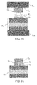
- the sintering operation is then carried out by pressing with a glass plate (the intermediate piece Ei) on the dried pulp with a pressure of 12 MPa and a temperature of 280 ° C. for 200 seconds, as illustrated in FIG. figure 2a to form the first elementary seal J1, the heat source being referenced S ch .
- These conditions make it possible to have a good adhesion between the gasket and the Cu layer with a measured shear stiffness of 28 MPa (by attaching an Ag finish Si chip). It should be noted that by testing at pressures of 9 MPa and 6 MPa, the Applicant has found decreases in shear stiffness of 50% and 80%.
- the glass plate Ei is easily detached from the first elementary seal thus formed and having a first density.
- a second layer of a paste P2 containing silver nanoparticles and compatible with the Ag and Au finishes is deposited by screen printing on the first sintered elementary seal (sintered joint J1), as illustrated in FIG. figure 2b .
- the chip Si (Ag finish), ie the element E2 with a topcoat C2 is then placed on the Ag paste and a sintering cycle at a temperature of 250 ° C. with a very low pressure (typically less than 0.1 MPa) is achieved (the heat source being referenced Sch).
- a very low pressure typically less than 0.1 MPa
- the modest pressure applied ensures good contact between the dough and the chip.
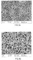
- the density of this layer can be controlled through the temperature rise ramp as shown by the SEM images of the Figures 3a, 3b and 3c taken respectively at the end of ramps of 6, 15 and 30 ° C / min.
- the decrease in the joint density and the increase in the size and number of pores in the joint observed by increasing the temperature ramp are initially related to the evaporation of the solvent, the binder and the dispersant (used for dough formation) during sintering. Under very fast ramps of temperature rise, the volatile products do not have time to escape from the joint before the beginning of sintering and their evaporation during the process will lead to the creation of numerous and large pores.
- the Figure 2c illustrates the assembly thus produced comprising a heterogeneous seal resulting from the stacking of the first elementary seal J1 and the second elementary seal J2 for assembling the elements E1 and E2.
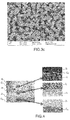
- This figure 4 represents a sectional view of a joint made in two steps and showing the two layers relating to the first elementary joint J1 and the second elementary joint J2 with different densities forming the final joint and connecting the Cu layer of the DBC and the silicon diode If, via the layer C2.
- This structure shows an average stiffness of 19 MPa using the same sintering conditions as those for Au and Cu topcoats (250 ° C and a ramp of 30 ° C / min). After the shear test, the observations show a delamination on the Ag metallization layer of the chip.
- a high pressure (12 MPa) sintering test of P1 paste on a Cu topcoat gives the best shear stiffness with an average value of 28 MPa.
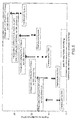
- the figure 5 shows the variation of the mechanical rigidity of the chips using several topcoat materials and the different sintering conditions already mentioned.
- the interface with the lowest adhesion is indicated.
- three samples were tested in order to have an acceptable statistic and are illustrated by three black squares represented in figure 5 .
- the method of assembly with the pulp 1 with a pressure of 12 MPa makes it possible to have the best rigidity in shear.
- this method is not compatible with components that are sensitive to high pressures and the joint is very dense (high Young's modulus) which can lead to high stresses on semiconductor metallizations during thermal cycling (difference in CTE between the Si and the DBC).
- the figure 6 shows an example of the delamination of the Ni-Ag layer (generally used as back-side metallization of the components) of a Si chip attached to a Cu-finished DBC after 700 thermal cycles between -40 ° C and 160 ° C using a seal dense J (seal 1 of the figure 4 ).
- thermomechanical reliability can be delayed or even avoided by using the developed structure of the present invention to obtain a relatively low density seal in contact with the semiconductor. This induces a lower Young's modulus and consequently a better collection of thermomechanical stresses resulting in a better seal reliability.
- Step 1
- a pressure sintered dough is used for the second deposit (such a dough is generally less expensive and more easily deposited by screen printing) while weakly pressing on the chip.
- this type of sintered pressure dough requires drying to remove the organic binders, which is not the case of the sintered dough without pressure.
- This drying step when followed by a low pressure assembly process, has mechanical weakness (the rupture zone) at the seal / chip interface.
Landscapes
- Chemical & Material Sciences (AREA)
- Engineering & Computer Science (AREA)
- Ceramic Engineering (AREA)
- Materials Engineering (AREA)
- Composite Materials (AREA)
- Manufacturing & Machinery (AREA)
- Mechanical Engineering (AREA)
- Structural Engineering (AREA)
- Organic Chemistry (AREA)
- Powder Metallurgy (AREA)
- Die Bonding (AREA)
Applications Claiming Priority (1)
| Application Number | Priority Date | Filing Date | Title |
|---|---|---|---|
| FR1556573A FR3038535B1 (fr) | 2015-07-10 | 2015-07-10 | Assemblage comprenant deux elements de coefficient de dilatation thermique differents et un joint fritte heterogene en densite et procede de fabrication de l'assemblage |
Publications (1)
| Publication Number | Publication Date |
|---|---|
| EP3115128A1 true EP3115128A1 (de) | 2017-01-11 |
Family
ID=54545246
Family Applications (1)
| Application Number | Title | Priority Date | Filing Date |
|---|---|---|---|
| EP16178287.5A Withdrawn EP3115128A1 (de) | 2015-07-10 | 2016-07-07 | Anordnung, die zwei elemente mit unterschiedlichen wärmeausdehnungskoeffizienten und eine sinterdichtung mit heterogener dichte umfasst, und herstellungsverfahren dieser anordnung |
Country Status (3)
| Country | Link |
|---|---|
| US (1) | US20170012017A1 (de) |
| EP (1) | EP3115128A1 (de) |
| FR (1) | FR3038535B1 (de) |
Cited By (1)
| Publication number | Priority date | Publication date | Assignee | Title |
|---|---|---|---|---|
| WO2024228183A1 (en) * | 2023-05-02 | 2024-11-07 | Inpack Technologies - Limited Partnership | Method of forming electrically conductive lines with controlled coefficient of thermal expansion |
Families Citing this family (5)
| Publication number | Priority date | Publication date | Assignee | Title |
|---|---|---|---|---|
| US11004680B2 (en) | 2016-11-26 | 2021-05-11 | Texas Instruments Incorporated | Semiconductor device package thermal conduit |
| US20180166369A1 (en) * | 2016-12-14 | 2018-06-14 | Texas Instruments Incorporated | Bi-Layer Nanoparticle Adhesion Film |
| US9865527B1 (en) | 2016-12-22 | 2018-01-09 | Texas Instruments Incorporated | Packaged semiconductor device having nanoparticle adhesion layer patterned into zones of electrical conductance and insulation |
| US9941194B1 (en) | 2017-02-21 | 2018-04-10 | Texas Instruments Incorporated | Packaged semiconductor device having patterned conductance dual-material nanoparticle adhesion layer |
| JP7130445B2 (ja) * | 2018-06-05 | 2022-09-05 | 新光電気工業株式会社 | 半導体装置及び半導体装置の製造方法 |
Citations (5)
| Publication number | Priority date | Publication date | Assignee | Title |
|---|---|---|---|---|
| US20060272700A1 (en) * | 2005-06-07 | 2006-12-07 | Young Richard J S | Aluminum thick film composition(s), electrode(s), semiconductor device(s) and methods of making thereof |
| EP2113583A1 (de) * | 2008-04-28 | 2009-11-04 | The Boeing Company | Zusammengesetzte Verbundstrukturen mit einem abgestuften Wärmeausdehnungskoeffizienten für Extremumgebungsanwendungen |
| US8257795B2 (en) | 2004-02-18 | 2012-09-04 | Virginia Tech Intellectual Properties, Inc. | Nanoscale metal paste for interconnect and method of use |
| JP2014127535A (ja) * | 2012-12-26 | 2014-07-07 | Hitachi Power Semiconductor Device Ltd | 半導体モジュール、及び半導体モジュールの製造方法 |
| US20140374775A1 (en) * | 2012-08-17 | 2014-12-25 | Fuji Electric Co., Ltd. | Electronic component and manufacturing method for electronic component |
Family Cites Families (5)
| Publication number | Priority date | Publication date | Assignee | Title |
|---|---|---|---|---|
| US5561321A (en) * | 1992-07-03 | 1996-10-01 | Noritake Co., Ltd. | Ceramic-metal composite structure and process of producing same |
| US7482638B2 (en) * | 2003-08-29 | 2009-01-27 | Philips Lumileds Lighting Company, Llc | Package for a semiconductor light emitting device |
| JP2008153470A (ja) * | 2006-12-18 | 2008-07-03 | Renesas Technology Corp | 半導体装置および半導体装置の製造方法 |
| JP2013038330A (ja) * | 2011-08-10 | 2013-02-21 | Toshiba Corp | 半導体装置の製造方法及び半導体装置 |
| US20130155629A1 (en) * | 2011-12-19 | 2013-06-20 | Tong Hsing Electronic Industries, Ltd. | Hermetic Semiconductor Package Structure and Method for Manufacturing the same |
-
2015
- 2015-07-10 FR FR1556573A patent/FR3038535B1/fr not_active Expired - Fee Related
-
2016
- 2016-07-07 EP EP16178287.5A patent/EP3115128A1/de not_active Withdrawn
- 2016-07-08 US US15/205,273 patent/US20170012017A1/en not_active Abandoned
Patent Citations (5)
| Publication number | Priority date | Publication date | Assignee | Title |
|---|---|---|---|---|
| US8257795B2 (en) | 2004-02-18 | 2012-09-04 | Virginia Tech Intellectual Properties, Inc. | Nanoscale metal paste for interconnect and method of use |
| US20060272700A1 (en) * | 2005-06-07 | 2006-12-07 | Young Richard J S | Aluminum thick film composition(s), electrode(s), semiconductor device(s) and methods of making thereof |
| EP2113583A1 (de) * | 2008-04-28 | 2009-11-04 | The Boeing Company | Zusammengesetzte Verbundstrukturen mit einem abgestuften Wärmeausdehnungskoeffizienten für Extremumgebungsanwendungen |
| US20140374775A1 (en) * | 2012-08-17 | 2014-12-25 | Fuji Electric Co., Ltd. | Electronic component and manufacturing method for electronic component |
| JP2014127535A (ja) * | 2012-12-26 | 2014-07-07 | Hitachi Power Semiconductor Device Ltd | 半導体モジュール、及び半導体モジュールの製造方法 |
Non-Patent Citations (4)
| Title |
|---|
| CACCURI ET AL.: "Mechanical Properties of Sintered Ag as a New Material for Die Bonding: Influence of the Density", JOURNAL OF ELECTRONIC MATERIALS, vol. 43, no. 12, 2014 |
| KNOERR ET AL.: "Power semiconductor joining through sintering of silver nanoparticles : Evaluation of influence of parameters time, temperature and pressure on density-strength and reliability", INTERNATIONAL CONFÉRENCE ON INTEGRATED POWER ELECTRONICS SYSTEMS CIPS, 16 March 2010 (2010-03-16) |
| LEI T G ET AL: "Low-Temperature Sintering of Nanoscale Silver Paste for Attaching Large-Area (>100 mm2) Chips", IEEE TRANSACTIONS ON COMPONENTS AND PACKAGING TECHNOLOGIES, IEEE SERVICE CENTER, PISCATAWAY, NJ, US, vol. 33, no. 1, 1 March 2010 (2010-03-01), pages 98 - 104, XP011346976, ISSN: 1521-3331, DOI: 10.1109/TCAPT.2009.2021256 * |
| ZHANG ET AL.: "Pressure-Assisted Low-Temperature Sintering of Silver Paste as an Alternative Die-Attach Solution to Solder reflow", IEEE TRANSACTIONS ON ELECTRONICS PACKAGING MANUFACTURING, vol. 25, no. 4, October 2002 (2002-10-01), pages 279 - 283 |
Cited By (1)
| Publication number | Priority date | Publication date | Assignee | Title |
|---|---|---|---|---|
| WO2024228183A1 (en) * | 2023-05-02 | 2024-11-07 | Inpack Technologies - Limited Partnership | Method of forming electrically conductive lines with controlled coefficient of thermal expansion |
Also Published As
| Publication number | Publication date |
|---|---|
| FR3038535A1 (fr) | 2017-01-13 |
| FR3038535B1 (fr) | 2017-08-11 |
| US20170012017A1 (en) | 2017-01-12 |
Similar Documents
| Publication | Publication Date | Title |
|---|---|---|
| EP3115128A1 (de) | Anordnung, die zwei elemente mit unterschiedlichen wärmeausdehnungskoeffizienten und eine sinterdichtung mit heterogener dichte umfasst, und herstellungsverfahren dieser anordnung | |
| EP2175485B1 (de) | Lötverbindung zwischen zwei ineinandergreifenden Steckern, und Verfahren zur deren Herstellung | |
| WO2017129687A1 (fr) | Assemblage comprenant des moyens d'interconnexion mixtes comportant des elements intermediaires d'interconnexion et des joints frittes metalliques et procede de fabrication | |
| EP3031076B1 (de) | Verfahren zur herstellung einer halbleiterstruktur mit vorläufiger bindung durch metallschichten | |
| JP4635230B2 (ja) | 接合方法及び接合構造 | |
| EP3115129B1 (de) | Anordnung, die ein für die wärmeübertragung geeignetes element, einen gut wärmeleitenden und elektrisch isolierenden polymerfilm, eine sinterdichtung und einen heizkörper umfasst, sowie entsprechendes herstellungsverfahren | |
| EP0662721A1 (de) | Elektromagnetischer Strahlungsdetektor und Herstellungsverfahren | |
| EP2126969B1 (de) | Verfahren zur verbindung elektronischer wafer | |
| FR2977178A1 (fr) | Procede de fabrication d'un dispositif comprenant des brasures realisees a partir d'oxalate metallique | |
| Rantamäki et al. | Low temperature gold-to-gold bonded semiconductor disk laser | |
| EP3351064B1 (de) | Montageverfahren durch silbersintern ohne druck | |
| EP2693468B1 (de) | Verfahren vom Typ Flip-Chip zum Zusammenbauen zweier elektronischer Bauteile | |
| JP5955183B2 (ja) | 半導体素子のダイボンド接合構造及び半導体素子のダイボンド接合方法 | |
| FR3021670B1 (fr) | Procede d'assemblage permanent de deux elements par interdiffusion en phase liquide transitoire | |
| FR3054721A1 (fr) | Module electronique de puissance d'un aeronef et procede de fabrication associe | |
| WO2014049551A1 (fr) | Procede d'assemblage de deux composants electroniques, de type flip-chip, assemblage obtenu selon le procede | |
| WO2017009586A1 (fr) | Procede de brasage par frittage d'une poudre conductrice par thermo-compression ultrasonique et module electronique de puissance realise par ce procede | |
| JP2024174434A (ja) | 導電性接合材料及び導電性接合材料の製造方法並びに接合部材 | |
| JP4333634B2 (ja) | シリコンウェハーの接合方法 | |
| WO2025257075A1 (fr) | Dispositif d'encapsulation et son procédé de fabrication | |
| FR3139411A1 (fr) | Boîtier de circuit integre | |
| WO2024134059A1 (fr) | Procédé de scellement eutectique de deux substrats | |
| EP3031775A1 (de) | Verfahren zur herstellung einer elektrischen verbindung in einem sackloch, und so erhaltene elektrische verbindung | |
| WO2021111067A1 (fr) | Procede de depot localise d'un materiau sur un element metallique | |
| Clayton | Adhesive Flip Chip for Large Arrayed Devices |
Legal Events
| Date | Code | Title | Description |
|---|---|---|---|
| PUAI | Public reference made under article 153(3) epc to a published international application that has entered the european phase |
Free format text: ORIGINAL CODE: 0009012 |
|
| STAA | Information on the status of an ep patent application or granted ep patent |
Free format text: STATUS: REQUEST FOR EXAMINATION WAS MADE |
|
| 17P | Request for examination filed |
Effective date: 20160707 |
|
| AK | Designated contracting states |
Kind code of ref document: A1 Designated state(s): AL AT BE BG CH CY CZ DE DK EE ES FI FR GB GR HR HU IE IS IT LI LT LU LV MC MK MT NL NO PL PT RO RS SE SI SK SM TR |
|
| AX | Request for extension of the european patent |
Extension state: BA ME |
|
| STAA | Information on the status of an ep patent application or granted ep patent |
Free format text: STATUS: EXAMINATION IS IN PROGRESS |
|
| 17Q | First examination report despatched |
Effective date: 20190313 |
|
| RIC1 | Information provided on ipc code assigned before grant |
Ipc: C04B 37/02 20060101ALI20191011BHEP Ipc: B22F 7/06 20060101ALI20191011BHEP Ipc: B22F 7/08 20060101ALI20191011BHEP Ipc: B22F 3/10 20060101AFI20191011BHEP Ipc: H01L 23/00 20060101ALI20191011BHEP Ipc: H01L 23/373 20060101ALI20191011BHEP Ipc: B22F 1/00 20060101ALI20191011BHEP Ipc: H01L 23/488 20060101ALI20191011BHEP |
|
| STAA | Information on the status of an ep patent application or granted ep patent |
Free format text: STATUS: THE APPLICATION IS DEEMED TO BE WITHDRAWN |
|
| 18D | Application deemed to be withdrawn |
Effective date: 20220201 |