EP3122805B1 - Articles transparents contenant une protection contre le rayonnement électromagnétique - Google Patents
Articles transparents contenant une protection contre le rayonnement électromagnétique Download PDFInfo
- Publication number
- EP3122805B1 EP3122805B1 EP15715852.8A EP15715852A EP3122805B1 EP 3122805 B1 EP3122805 B1 EP 3122805B1 EP 15715852 A EP15715852 A EP 15715852A EP 3122805 B1 EP3122805 B1 EP 3122805B1
- Authority
- EP
- European Patent Office
- Prior art keywords
- panel
- substrate
- viewing panel
- conductive coating
- conductive
- Prior art date
- Legal status (The legal status is an assumption and is not a legal conclusion. Google has not performed a legal analysis and makes no representation as to the accuracy of the status listed.)
- Not-in-force
Links
Images


Classifications
-
- H—ELECTRICITY
- H05—ELECTRIC TECHNIQUES NOT OTHERWISE PROVIDED FOR
- H05B—ELECTRIC HEATING; ELECTRIC LIGHT SOURCES NOT OTHERWISE PROVIDED FOR; CIRCUIT ARRANGEMENTS FOR ELECTRIC LIGHT SOURCES, IN GENERAL
- H05B6/00—Heating by electric, magnetic or electromagnetic fields
- H05B6/64—Heating using microwaves
- H05B6/76—Prevention of microwave leakage, e.g. door sealings
- H05B6/766—Microwave radiation screens for windows
-
- C—CHEMISTRY; METALLURGY
- C08—ORGANIC MACROMOLECULAR COMPOUNDS; THEIR PREPARATION OR CHEMICAL WORKING-UP; COMPOSITIONS BASED THEREON
- C08J—WORKING-UP; GENERAL PROCESSES OF COMPOUNDING; AFTER-TREATMENT NOT COVERED BY SUBCLASSES C08B, C08C, C08F, C08G or C08H
- C08J7/00—Chemical treatment or coating of shaped articles made of macromolecular substances
- C08J7/04—Coating
-
- B—PERFORMING OPERATIONS; TRANSPORTING
- B32—LAYERED PRODUCTS
- B32B—LAYERED PRODUCTS, i.e. PRODUCTS BUILT-UP OF STRATA OF FLAT OR NON-FLAT, e.g. CELLULAR OR HONEYCOMB, FORM
- B32B17/00—Layered products essentially comprising sheet glass, or glass, slag, or like fibres
- B32B17/06—Layered products essentially comprising sheet glass, or glass, slag, or like fibres comprising glass as the main or only constituent of a layer, next to another layer of a specific material
-
- B—PERFORMING OPERATIONS; TRANSPORTING
- B32—LAYERED PRODUCTS
- B32B—LAYERED PRODUCTS, i.e. PRODUCTS BUILT-UP OF STRATA OF FLAT OR NON-FLAT, e.g. CELLULAR OR HONEYCOMB, FORM
- B32B33/00—Layered products characterised by particular properties or particular surface features, e.g. particular surface coatings; Layered products designed for particular purposes not covered by another single class
-
- C—CHEMISTRY; METALLURGY
- C03—GLASS; MINERAL OR SLAG WOOL
- C03C—CHEMICAL COMPOSITION OF GLASSES, GLAZES OR VITREOUS ENAMELS; SURFACE TREATMENT OF GLASS; SURFACE TREATMENT OF FIBRES OR FILAMENTS MADE FROM GLASS, MINERALS OR SLAGS; JOINING GLASS TO GLASS OR OTHER MATERIALS
- C03C17/00—Surface treatment of glass, not in the form of fibres or filaments, by coating
-
- C—CHEMISTRY; METALLURGY
- C03—GLASS; MINERAL OR SLAG WOOL
- C03C—CHEMICAL COMPOSITION OF GLASSES, GLAZES OR VITREOUS ENAMELS; SURFACE TREATMENT OF GLASS; SURFACE TREATMENT OF FIBRES OR FILAMENTS MADE FROM GLASS, MINERALS OR SLAGS; JOINING GLASS TO GLASS OR OTHER MATERIALS
- C03C17/00—Surface treatment of glass, not in the form of fibres or filaments, by coating
- C03C17/006—Surface treatment of glass, not in the form of fibres or filaments, by coating with materials of composite character
- C03C17/008—Surface treatment of glass, not in the form of fibres or filaments, by coating with materials of composite character comprising a mixture of materials covered by two or more of the groups C03C17/02, C03C17/06, C03C17/22 and C03C17/28
-
- C—CHEMISTRY; METALLURGY
- C03—GLASS; MINERAL OR SLAG WOOL
- C03C—CHEMICAL COMPOSITION OF GLASSES, GLAZES OR VITREOUS ENAMELS; SURFACE TREATMENT OF GLASS; SURFACE TREATMENT OF FIBRES OR FILAMENTS MADE FROM GLASS, MINERALS OR SLAGS; JOINING GLASS TO GLASS OR OTHER MATERIALS
- C03C17/00—Surface treatment of glass, not in the form of fibres or filaments, by coating
- C03C17/06—Surface treatment of glass, not in the form of fibres or filaments, by coating with metals
-
- C—CHEMISTRY; METALLURGY
- C03—GLASS; MINERAL OR SLAG WOOL
- C03C—CHEMICAL COMPOSITION OF GLASSES, GLAZES OR VITREOUS ENAMELS; SURFACE TREATMENT OF GLASS; SURFACE TREATMENT OF FIBRES OR FILAMENTS MADE FROM GLASS, MINERALS OR SLAGS; JOINING GLASS TO GLASS OR OTHER MATERIALS
- C03C17/00—Surface treatment of glass, not in the form of fibres or filaments, by coating
- C03C17/22—Surface treatment of glass, not in the form of fibres or filaments, by coating with other inorganic material
-
- C—CHEMISTRY; METALLURGY
- C08—ORGANIC MACROMOLECULAR COMPOUNDS; THEIR PREPARATION OR CHEMICAL WORKING-UP; COMPOSITIONS BASED THEREON
- C08J—WORKING-UP; GENERAL PROCESSES OF COMPOUNDING; AFTER-TREATMENT NOT COVERED BY SUBCLASSES C08B, C08C, C08F, C08G or C08H
- C08J7/00—Chemical treatment or coating of shaped articles made of macromolecular substances
- C08J7/04—Coating
- C08J7/043—Improving the adhesiveness of the coatings per se, e.g. forming primers
-
- C—CHEMISTRY; METALLURGY
- C08—ORGANIC MACROMOLECULAR COMPOUNDS; THEIR PREPARATION OR CHEMICAL WORKING-UP; COMPOSITIONS BASED THEREON
- C08J—WORKING-UP; GENERAL PROCESSES OF COMPOUNDING; AFTER-TREATMENT NOT COVERED BY SUBCLASSES C08B, C08C, C08F, C08G or C08H
- C08J7/00—Chemical treatment or coating of shaped articles made of macromolecular substances
- C08J7/04—Coating
- C08J7/044—Forming conductive coatings; Forming coatings having anti-static properties
-
- C—CHEMISTRY; METALLURGY
- C08—ORGANIC MACROMOLECULAR COMPOUNDS; THEIR PREPARATION OR CHEMICAL WORKING-UP; COMPOSITIONS BASED THEREON
- C08J—WORKING-UP; GENERAL PROCESSES OF COMPOUNDING; AFTER-TREATMENT NOT COVERED BY SUBCLASSES C08B, C08C, C08F, C08G or C08H
- C08J7/00—Chemical treatment or coating of shaped articles made of macromolecular substances
- C08J7/04—Coating
- C08J7/046—Forming abrasion-resistant coatings; Forming surface-hardening coatings
-
- C—CHEMISTRY; METALLURGY
- C09—DYES; PAINTS; POLISHES; NATURAL RESINS; ADHESIVES; COMPOSITIONS NOT OTHERWISE PROVIDED FOR; APPLICATIONS OF MATERIALS NOT OTHERWISE PROVIDED FOR
- C09D—COATING COMPOSITIONS, e.g. PAINTS, VARNISHES OR LACQUERS; FILLING PASTES; CHEMICAL PAINT OR INK REMOVERS; INKS; CORRECTING FLUIDS; WOODSTAINS; PASTES OR SOLIDS FOR COLOURING OR PRINTING; USE OF MATERIALS THEREFOR
- C09D5/00—Coating compositions, e.g. paints, varnishes or lacquers, characterised by their physical nature or the effects produced; Filling pastes
- C09D5/24—Electrically-conducting paints
-
- B—PERFORMING OPERATIONS; TRANSPORTING
- B32—LAYERED PRODUCTS
- B32B—LAYERED PRODUCTS, i.e. PRODUCTS BUILT-UP OF STRATA OF FLAT OR NON-FLAT, e.g. CELLULAR OR HONEYCOMB, FORM
- B32B2307/00—Properties of the layers or laminate
- B32B2307/20—Properties of the layers or laminate having particular electrical or magnetic properties, e.g. piezoelectric
- B32B2307/212—Electromagnetic interference shielding
-
- C—CHEMISTRY; METALLURGY
- C03—GLASS; MINERAL OR SLAG WOOL
- C03C—CHEMICAL COMPOSITION OF GLASSES, GLAZES OR VITREOUS ENAMELS; SURFACE TREATMENT OF GLASS; SURFACE TREATMENT OF FIBRES OR FILAMENTS MADE FROM GLASS, MINERALS OR SLAGS; JOINING GLASS TO GLASS OR OTHER MATERIALS
- C03C2217/00—Coatings on glass
- C03C2217/20—Materials for coating a single layer on glass
- C03C2217/25—Metals
-
- C—CHEMISTRY; METALLURGY
- C03—GLASS; MINERAL OR SLAG WOOL
- C03C—CHEMICAL COMPOSITION OF GLASSES, GLAZES OR VITREOUS ENAMELS; SURFACE TREATMENT OF GLASS; SURFACE TREATMENT OF FIBRES OR FILAMENTS MADE FROM GLASS, MINERALS OR SLAGS; JOINING GLASS TO GLASS OR OTHER MATERIALS
- C03C2217/00—Coatings on glass
- C03C2217/20—Materials for coating a single layer on glass
- C03C2217/28—Other inorganic materials
-
- C—CHEMISTRY; METALLURGY
- C03—GLASS; MINERAL OR SLAG WOOL
- C03C—CHEMICAL COMPOSITION OF GLASSES, GLAZES OR VITREOUS ENAMELS; SURFACE TREATMENT OF GLASS; SURFACE TREATMENT OF FIBRES OR FILAMENTS MADE FROM GLASS, MINERALS OR SLAGS; JOINING GLASS TO GLASS OR OTHER MATERIALS
- C03C2217/00—Coatings on glass
- C03C2217/20—Materials for coating a single layer on glass
- C03C2217/29—Mixtures
-
- C—CHEMISTRY; METALLURGY
- C08—ORGANIC MACROMOLECULAR COMPOUNDS; THEIR PREPARATION OR CHEMICAL WORKING-UP; COMPOSITIONS BASED THEREON
- C08J—WORKING-UP; GENERAL PROCESSES OF COMPOUNDING; AFTER-TREATMENT NOT COVERED BY SUBCLASSES C08B, C08C, C08F, C08G or C08H
- C08J2300/00—Characterised by the use of unspecified polymers
- C08J2300/12—Polymers characterised by physical features, e.g. anisotropy, viscosity or electrical conductivity
-
- C—CHEMISTRY; METALLURGY
- C08—ORGANIC MACROMOLECULAR COMPOUNDS; THEIR PREPARATION OR CHEMICAL WORKING-UP; COMPOSITIONS BASED THEREON
- C08J—WORKING-UP; GENERAL PROCESSES OF COMPOUNDING; AFTER-TREATMENT NOT COVERED BY SUBCLASSES C08B, C08C, C08F, C08G or C08H
- C08J2367/00—Characterised by the use of polyesters obtained by reactions forming a carboxylic ester link in the main chain; Derivatives of such polymers
- C08J2367/02—Polyesters derived from dicarboxylic acids and dihydroxy compounds
Definitions
- Microwave oven door viewing panels made of glass panes can require electromagnetic interference (EMI) shielding to limit EMI from transmission outside the oven cavity to meet industry and/or governmental regulations.
- Metal can be a good EMI shielding material.
- a viewing panel can incorporate a metal sheet to limit transmission of EMI through the panel.
- the metal sheet can be perforated which can improve visibility through the panel while maintaining the shielding functionality.
- a perforated metal sheet incorporated into a viewing panel of a microwave oven door can effectively limit transmission of microwaves through the viewing panel and can meet industry and/or governmental standards for microwave transmission.
- a perforated metal sheet can limit transmission of light visible to the human eye, e.g., EMI having a frequency of 430 terahertz (THz) to 790 THz, or wavelengths in air of 390 nanometer (nm) to 700 nm.
- EMI having a frequency of 430 terahertz (THz) to 790 THz, or wavelengths in air of 390 nanometer (nm) to 700 nm.
- EMI having a perforated metal sheet
- a viewing panel having a perforated metal sheet can obscure the image of a food item placed inside a microwave oven cavity which can be undesirable to consumers.
- visibility visible light transmittance through the panel
- microwave shielding Larger perforations can render the microwave shielding unsatisfactory, while small perforations can reduce visibility.
- a perforated metal sheet can increase the weight of a microwave oven door assembly.
- a stronger hinge can be used, which can further increase the weight and cost of the microwave oven.
- viewing panels having a perforated metal sheet and a glass pane can be limited to flat construction due at least in part to relatively high cost associated with forming each component into alternative shape and assembling them together. Thus, incorporating such construction into a microwave oven can limit design freedom.
- a method of forming a viewing panel for a microwave oven can comprise: placing a film including a conductive coating into a mold and molding a substrate to a surface of the film having the conductive coating to form the viewing panel; or injection molding a substrate and applying a conductive coating to a surface of the substrate after molding to form the viewing panel; wherein the substrate is selected from a transparent polymer or glass; the conductive coating has an EMI shielding effectiveness of greater than 25 dB from 30 MHz to 3.0 GHz as determined by ASTM D4935; and the viewing panel has a transmittance of greater than or equal to 50% of incident light having a frequency of 430 THz to 790 THz.
- a method of forming a viewing panel for a microwave oven can comprise: coupling a film including a conductive coating to a substrate to form a panel preform; and thermoforming or vacuum forming the panel preform to form the viewing panel; wherein the substrate is selected from a transparent polymer or glass; the coating has a surface resistance of less than or equal to 1.0 ohm/sq; and the viewing panel has a transmittance of greater than or equal to 50% of incident light having a frequency of 430 THz to 790 THz.
- a viewing panel for a microwave oven can comprise: a substrate comprising a transparent polymer or glass; a conductive coating adjacent to a surface of the substrate; wherein the coating includes conductive nanoparticles selected from conductive nanoparticles, conductive metal nanowire, carbon allotropes, or a combination comprising at least one of the foregoing, wherein the conductive nanoparticles are nanometer sized metal particles arranged in a network; the viewing panel has a transmittance of greater than or equal to 50% of incident light having a frequency of 430 THz to 790 THz; and the viewing panel has an EMI shielding effectiveness of greater than 25 dB from 30 MHz to 3.0 GHz as determined by ASTM D4935.
- a microwave oven can cook food items placed within an oven cavity by subjecting them to microwaves, e.g., electromagnetic interference (EMI) having a frequency of 300 gigahertz (GHz) to 300 megahertz (MHz).
- EMI electromagnetic interference
- a magnetron, or similar device, for converting electrical energy into EMI can feed the microwaves into the oven cavity.
- a metal plate, or metal coated surfaces can be disposed along the walls of the microwave oven cavity and can confine the microwaves within the oven cavity.
- a door for accessing the oven cavity can be disposed on a wall of the oven.
- a viewing panel e.g., a window
- Microwave transmission from the surfaces of a microwave oven can be regulated by industry, international, and/or governmental codes and standards (e.g. 21CFR1030.10 revised April 1, 2013, International Special Committee on Radio Interference (CISPR) 11, CISPR 19, Federal Communications Commission (FCC) part 18, European Standard EN55011, and similar standards).
- a lighter weight microwave oven viewing panel including a transparent substrate, e.g., a transparent polymeric substrate or a transparent glass substrate, and a conductive coating where the viewing panel has increased visible light transmittance as compared to a microwave oven viewing panel made of glass and a metal sheet for EMI shielding is disclosed.
- the viewing panel also has sufficient microwave shielding capability (i.e., EMI shielding in the microwave frequency) to meet relevant national and industry standards for microwave emission and can provide greater design freedom allowing for improved aesthetics and curved designs.
- the conductive coating can be disposed adjacent to a surface of the substrate.
- the conductive coating can be coupled directly to a surface of the substrate.
- the conductive coating can be coupled to the surface of a polymer film coupled to a surface of the substrate.
- a conductive coating e.g., a transparent conductive coating
- the coating can have a transmittance of visible light of greater than 50%, for example, greater than 60%, for example, greater than 70%.
- the conductive coating can be continuously conductive.
- the conductive coating can have a sheet resistance of less than 50 Ohms per square ( ⁇ /sq), for example, less than 25 ⁇ /sq, for example, less than 10 ⁇ /sq, for example, less than 1 ⁇ /sq.
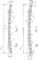
- FIG. 1 is an illustration of a cross-section of a viewing panel 2.
- the viewing panel 2 can include a substrate 6 and a conductive coating 4, where the substrate 6 can include an inside surface 14 and an outside surface 12.
- the conductive coating 4 can be adjacent to the outside surface 12 of the substrate 6.
- a conductive coating can be adjacent to the inside surface 14 of the substrate 6.
- the conductive coating 4 can be applied directly to the surfaces 12, 14 of the substrate 6.
- the viewing panel 2 can be curved in at least one dimension, e.g., the w-axis dimension.
- the viewing panel 2 can be curved in two dimensions, e.g., the w-axis and h-axis dimensions.
- the viewing panel 2 can have a width, W, measured along a w-axis.
- the viewing panel 2 can have a depth, D, measured along a d-axis.
- the depth, D can be larger than the total thickness, T, of the viewing panel.
- the depth of the viewing panel at a centroid 16 can be larger than a depth, D p , at a point along the perimeter of the viewing panel 2.
- the depth, D can be larger than twice the total thickness, T, of the viewing panel 2.
- the depth, D, of the viewing panel 2 can be maximum at the centroid 16.
- the viewing panel 2 can have a maximum depth that is not coincident with the centroid 16.
- the conductive coating 4 can be dispersed across a portion of the width, W, of the substrate 6.
- the conductive coating 4 can be dispersed across the entire width, W, of the substrate 6.
- the conductive coating 4 can be dispersed across a portion of the height, H, of the substrate 6.
- the conductive coating 4 can be dispersed across the entire height, H, of the substrate 6.
- the conductive coating 4 can be dispersed across a portion of the outside surface 12 of the substrate 6.
- the conductive coating 4 can be dispersed across the entire outside surface 12 of the substrate 6.
- FIG. 2 is an illustration of a cross-section of a viewing panel 22.
- the viewing panel can include a substrate 6, a conductive coating 4, and a protective material 10, where the substrate 6 can include an inside surface 14 and an outside surface 12.
- the viewing panel 22 can be disposed adjacent to a conductive frame 20.
- a conductive frame 20 can abut a perimeter edge 18 of the viewing panel 22.
- a conductive frame 20 can extend along a portion of the perimeter of the viewing panel 22.
- a conductive frame 20 can extend along the entire perimeter of the viewing panel 2 such that it can surround the viewing panel 2.
- a conductive frame 20 can extend along a portion of the surfaces 12, 14 of the viewing panel 2.
- the conductive frame 20 can be in electrical communication with the conductive coating 4.
- the protective material 10 can be disposed adjacent to a surface 12, 14 of the substrate 6.
- the protective material 10 can provide an underlying layer with resistance to abrasion, ultraviolet radiation, microbes, bacteria, corrosion, or a combination comprising at least one of the foregoing
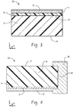
- FIG. 3 is an illustration of a cross-section of a portion of a viewing panel 32.
- the viewing panel 2 can include a film 8 with a conductive coating 4 disposed adjacent to a surface of the film 8, a substrate 6, and a protective material 10.
- the conductive coating 4 can be disposed on a surface of the film 8 disposed adjacent to the outside surface 12 of the substrate 6.
- the conductive coating 4 can be disposed on a surface of the film 8 opposite the surface disposed adjacent to the outside surface 12 of the substrate 6.
- the substrate 6 can be injection molded onto the film 8, such as by a film insert molding or similar processes.
- the conductive coating 4 can be applied to the film 8 and the film 8 layered onto a surface 12, 14 of the substrate 6.
- the substrate 6 and film 8, having a conductive coating 4 can be formed into a viewing panel 2 by a thermoforming, vacuum forming, or similar process.
- the protective material 10 can be applied to a surface of the viewing panel 2.
- a protective material 10 can be a wet coating.
- the protective material 10 can be applied using any suitable wet coating technique, e.g., roller coating, screen printing, spreading, spray coating, spin coating, dipping, and the like.
- a protective material 10 can be a film, or can be applied to a film, which can be adhered to a side of a viewing panel 2.
- a protective material 10 can be glass.
- An adhesion promoter can be incorporated into a film having a protective material 10 to improve adherence to a surface of the viewing panel 2.
- FIG. 4 is an illustration of a cross-section of a portion of a viewing panel 42.
- the viewing panel 42 can include a substrate 6 including an outside surface 12 and an inside surface 14 and a conductive coating 4 adjacent to a surface of the substrate.
- the conductive coating 4 can be applied directly to a surface 12, 14 of the substrate 6.
- the viewing panel 2 can abut a conductive frame 20.
- a conductive frame 20 can be in electrical communication with a conductive coating 4.
- the conductive frame 20 can extend along a portion of an outside surface 12 of the substrate 6 of the viewing panel 42.
- the conductive frame 20 can extend along a portion of an inside surface 14 of the substrate 6 of the viewing panel 42.
- the conductive frame 20 can abut a perimeter edge 18 of the viewing panel 42.
- the conductive frame 20 can extend along the entire perimeter edge 18 of the viewing panel 42 such that it can surround the viewing panel 42 (e.g., can extend along the entire perimeter edge 18 of the viewing panel 42 and can extend along a portion of the substrate and/or a portion of the conductive coating 4).
- a protective material 10 can be disposed adjacent to a surface 12, 14 of the substrate 6.
- a protective material 10 can be disposed on a surface 12, 14 of the substrate 6.
- a protective material 10 can be disposed adjacent to a conductive coating 4.
- a protective material 10 can be disposed along a portion of a surface of a conductive coating 4.
- the viewing panel 42 can be coupled to a conductive frame 20 using any mechanical or chemical attachment that can provide electrical connectivity between the conductive coating 4 and conductive frame 20 (e.g., electrically conductive adhesive, fastener, frictional fit).
- a substrate 6 can be injection molded onto a conductive frame 20 and a conductive coating 4 can be applied to a surface of the viewing panel 42.
- a conductive frame 20 can abut a conductive coating 4 along at least one dimension, e.g., d-axis dimension.
- a conductive frame 20 can abut a conductive coating 4 along two dimensions, e.g., d-axis dimension and w-axis dimension.
- a conductive frame 20 can abut a conductive coating 4 along three dimensions, e.g., d-axis dimension, w-axis dimension, and h-axis dimension.
- FIG. 5 is an illustration of a cross-section of a viewing panel 52.
- the viewing panel 52 can have a substrate 6 and conductive coating 4.
- the viewing panel 52 can have a height, H, measured along an h-axis dimension.
- the viewing panel 52 can have a width, W, measured along a w-axis dimension.
- the viewing panel 52 can have a depth, D, measured along a d-axis dimension.
- the conductive coating 4 can be adjacent to a surface of the substrate 6.
- the viewing panel 52 can be bent along an edge such that the viewing panel 2 is asymmetric along at least one axis, e.g., asymmetric about a centerline 24.
- Bent edges 26 on the substrate 6 and conductive coating 4 can provide a larger area for electrical communication between a conductive frame 20 and a conductive coating 4.
- the conductive coating 4 can be dispersed across a portion of the width, W, of the substrate 6.
- the conductive coating 4 can be dispersed across the entire width, W, of the substrate 6.
- the conductive coating 4 can be dispersed across a portion of the height, H, of the substrate 6.
- the conductive coating 4 can be dispersed across the entire height, H, of the substrate 6.
- FIG. 7 is an illustration of a microwave oven door 80 with a viewing panel 82 as described herein. It is to be understand that any of the viewing panels 2, 22, 32, 42, 52 as disclosed herein can be used with the microwave oven door 80 of FIG. 7 .
- the substrate can be formed by any forming process, e.g., a polymer forming process.
- the substrate can include a transparent material, e.g., glass or a polymeric substrate.
- a substrate can be formed by an extrusion, calendaring, molding (e.g., injection molding), thermoforming, vacuum forming, or other desirable forming process.
- the substrate can be made as a flat sheet.
- the substrate can be formed with curvature.
- the substrate can be formed such that it is not flat.
- the substrate can be formed such that it is not coplanar with a plane defined by the height and width dimensions of the substrate.
- the substrate can be formed with a curved shape such that a depth dimension exceeds a maximum thickness of the substrate (e.g., acknowledging that the thickness of the substrate can vary due to imperfections in manufacturing, such as tool tolerances, variations in process conditions such as temperature, variation in shrinkage during cooling, and the like).
- the substrate can be curved such that a portion of the substrate has a depth dimension greater than or equal to twice the average thickness of the panel.
- the substrate can be curved such that the depth of the substrate measured at the centroid of the substrate is greater than the depth of the substrate measured at a point along the perimeter of the substrate.
- the substrate can be curved such that a depth dimension of the substrate is largest at the centroid of the substrate.
- a film having a conductive coating can be layered onto a surface of a substrate to form a viewing panel.
- a conductive coating can be applied directly to a surface of a substrate to form a viewing panel.
- a film including a conductive coating can be placed in a mold and a polymer substrate can be injection molded to a surface of the film to form a viewing panel.
- a film, including a conductive coating can be layered onto a substrate (e.g., a polymer substrate) and the film and substrate can be thermoformed into a viewing panel. The film can have additional layers of conductive coatings attached to it.
- the film can have greater than or equal to 1 conductive coating layer, for example, the film can have greater than or equal to 2 conductive layers, for example, greater than or equal to 3 conductive coating layers, for example, greater than or equal to 5 conductive coating layers, for example, greater than or equal to 10 conductive coating layers, for example, greater than or equal to 15 conductive coating layers.
- the perimeter shape of the substrate can be any shape, e.g., circular, elliptical, or the shape of a polygon having straight or curved edges.
- a film can be adhered to the substrate formed using a thermoforming, vacuum forming, or similar process.
- the film can include an adhesion promoter.
- the film can be adhered to a substrate with an adhesive.
- the conductive coating can be applied to a substrate or film using any suitable wet coating technique.
- the conductive coating can be applied using screen printing, spreading, spray coating, spin coating, dipping, and the like.
- a substrate can be injection molded into a shape having a depth dimension that exceeds the thickness of the substrate and a conductive coating can be applied to a surface of the substrate.
- a conductive coating can be applied to a flat film, the flat film and the substrate can be positioned into a thermoforming tool which can form the film and substrate into a viewing panel having a depth dimension exceeding the total thickness (e.g., combined thickness of the film, coating, and substrate).
- the conductive coating can be formed from conductive nanoparticles, including conductive nanoparticles, conductive metal nanowires, carbon allotropes such as carbon nanotubes, graphene, etc., and combinations comprising at least one of the foregoing.
- Metal nanoparticles can include copper and silver nanoparticles.
- a metal mesh film can be used having a regular network. Transmittance can be about 70 to about 80% and resistance, measured in Ohm/square can be less than 0.5.
- Conductive coatings can be formed from conductive metal nanoparticles formed into a patterned network of conductive traces and transparent cells, i.e., voids having few nanoparticles.
- the network can be random or regular in shape, the transmittance can be about 70%, and the resistance can be less than 0.05 Ohm/square.
- the transparent cells can have sizes of less than 1 millimeter (mm), for example, less than 0.5 mm, for example, less than 0.25 mm.
- Transparent conductive coatings are described, for example, in U.S. Pat. No. 7,601,406 .
- the conductive coating (e.g., conductive metal nanoparticle layers) can be applied to substrate by several techniques, including, printing of conductive inks (e.g., flexographic, screen printing, inkjet, gravure), coating and patterning of e.g., silver halide emulsions which can be reduced to silver particles, coating of conductive nanowire dispersions, and self-assembly of silver nanoparticle dispersions or emulsions.
- conductive inks e.g., flexographic, screen printing, inkjet, gravure
- the conductive coating can contain an EMI shielding material.
- the conductive coating can include pure metals such as silver (Ag), nickel (Ni), copper (Cu), or similar shielding metal, metal oxides thereof, combinations comprising at least one of the foregoing, and metal alloys comprising at least one of the foregoing, or metals or metal alloys produced by the Metallurgic Chemical Process (MCP) described in U.S. Pat. No. 5,476,535 .
- Metal particles of the conductive coating can be nanometer sized, e.g., such as where 90% of the particles can have an equivalent spherical diameter of less than 100 nanometers (nm).
- the metals of the conductive coating can form a network of interconnected metal traces defining openings on the substrate surface to which it is applied.
- the surface resistance of the conductive coating can be less than or equal to 1.0 ohm per square (ohm/sq).
- a conductive coating can have an EMI shielding effectiveness from 30 megahertz (MHz) to 1.5 gigahertz (GHz) as determined per ASTM D4935 of greater than 25 decibel (dB), for example, 30 dB to 80 dB, or, 40 dB to 80 dB.
- the conductive coating can include carbon based particles arranged in a network, e.g., carbon based particle with a metal mesh.
- the conductive coating including carbon based particles can be arranged in a regular network.
- the conductive coating including carbon based particles can be arranged in an irregular network.
- the carbon based particles can include graphene, carbon nanotubes, or a combination comprising at least one of the foregoing.
- the substrate can be a glass substrate.
- the substrate can be a transparent polymer substrate where the transparent polymer substrate can include a thermoplastic resin, a thermoset resin, or a combination comprising at least one of the foregoing.
- the transparent polymer substrate and a film coupled to the substrate can include the same polymer material or can include different polymer materials.
- thermoplastic resins include, but are not limited to, oligomers, polymers, ionomers, dendrimers, copolymers such as graft copolymers, block copolymers (e.g., star block copolymers, random copolymers, and the like) or a combination comprising at least one of the foregoing.
- thermoplastic resins include, but are not limited to, polycarbonates (e.g., blends of polycarbonate (such as, polycarbonate-polybutadiene blends, copolyester polycarbonates)), polystyrenes (e.g., copolymers of polycarbonate and styrene, polyphenylene ether-polystyrene blends), polyimides (e.g., polyetherimides), acrylonitrile-styrene-butadiene (ABS), polyarylates, polyalkylmethacrylates (e.g., polymethylmethacrylates (PMMA)), polyesters (e.g., copolyesters, polythioesters), polyolefins (e.g., polypropylenes (PP) and polyethylenes, high density polyethylenes (HDPE), low density polyethylenes (LDPE), linear low density polyethylenes (LLDPE)), polyamides (e.g., polyamideimides),
- thermoplastic resin can include, but is not limited to, polycarbonate resins (e.g., LexanTM resins, commercially available from SABIC's Innovative Plastics business), polyphenylene ether-polystyrene resins (e.g., NorylTM resins, commercially available from SABIC's innovative Plastics business), polyetherimide resins (e.g., UltemTM resins, commercially available from SABIC's innovative Plastics business), polybutylene terephthalate-polycarbonate resins (e.g., XenoyTM resins, commercially available from SABIC's innovative Plastics business), copolyestercarbonate resins (e.g., LexanTM SLX resins, commercially available from SABIC's innovative Plastics business), or a combination comprising at least one of the foregoing resins.
- polycarbonate resins e.g., LexanTM resins, commercially available from SABIC's Innovative Plastics business
- thermoplastic resins can include, but are not limited to, homopolymers and copolymers of a polycarbonate, a polyester, a polyacrylate, a polyamide, a polyetherimide, a polyphenylene ether, or a combination comprising at least one of the foregoing resins.
- the polycarbonate can comprise copolymers of polycarbonate (e.g., polycarbonate-polysiloxane, such as polycarbonate-polysiloxane block copolymer), linear polycarbonate, branched polycarbonate, end-capped polycarbonate (e.g., nitrile end-capped polycarbonate), or a combination comprising at least one of the foregoing, for example, a combination of branched and linear polycarbonate.
- polycarbonate e.g., polycarbonate-polysiloxane, such as polycarbonate-polysiloxane block copolymer
- linear polycarbonate e.g., polycarbonate-polysiloxane, such as polycarbonate-polysiloxane block copolymer
- branched polycarbonate branched polycarbonate
- end-capped polycarbonate e.g., nitrile end-capped polycarbonate
- the transparent polymer substrate and/or film of the viewing panel can include various additives ordinarily incorporated into polymer compositions of this type, with the proviso that the additive(s) are selected so as to not significantly adversely affect the desired properties of the polymer, in particular, transparency, deflection, stress, and flexural stiffness.
- additives can be mixed at a suitable time during the mixing of the components for forming the substrate and/or film.
- Exemplary additives include impact modifiers, fillers, reinforcing agents, antioxidants, heat stabilizers, light stabilizers, ultraviolet (UV) light stabilizers, plasticizers, lubricants, mold release agents, antistatic agents, colorants (such as carbon black and organic dyes), surface effect additives, radiation stabilizers (e.g., infrared absorbing), flame retardants, and anti-drip agents.
- a combination of additives can be used, for example, a combination of a heat stabilizer, mold release agent, and ultraviolet light stabilizer.
- the total amount of additives (other than any impact modifier, filler, or reinforcing agents) can be 0.001 weight percent (wt%) to 5 wt%, based on the total weight of the composition of the substrate and/or film.
- the substrate can be pretreated to alter the surface energy or to enhance adhesion of the conductive coating using physical or chemical techniques such as ultraviolet (UV), corona, plasma, or chemical primers.
- UV ultraviolet
- corona corona
- plasma plasma
- chemical primers chemical primers
- the conductive coating (e.g., transparent, conductive coating) can be plated with an additional conductive metal layer to decrease electrical resistance.
- Plating techniques can include electroless and electroplating with conductive metals such as silver and copper. Plating techniques are described in U.S. Patent No. 8,105,472 and U.S. Patent Publication No. 2011/0003141 .
- the coating can be placed on the outside or inside of the window.
- the coating can be placed as a layer within a multilayer window, such as being sandwiched between two or more transparent substrates providing protection for the conductive network. Single layers of the transparent, conductive coating can be used, or multiple layers can be used, optionally with a space located therebetween.
- the transparent, conductive coating can cover the entire transparent portion of the window (e.g., 100%).
- the transparent, conductive coating can cover a portion (e.g., greater than or equal to 50%) of the window.
- the transparent, conductive coating can be grounded to the metallic door frame or chassis of the microwave oven.
- the electrical connection between the coating and metallic frame can be accomplished by various techniques, including, but not limited to conductive inks or pastes, conductive tape such as copper tape, soldered connections, or conductive adhesives.
- One end of the connection can be attached to the metallic door frame or chassis of the microwave oven, while the other end of the connection can be attached to the transparent, conductive coating.
- the electrical attachment to the coating can be done at multiple locations or even continuously around the perimeters to provide sufficient connection to all parts of the conductive network.
- the viewing panel can transmit greater than or equal to 50% (e.g., 50 percent transmittance) of incident EMI having a frequency of 430 THz to 790 THz, for example, 60% to 100%, or, 70% to 100%.
- a transparent polymer, substrate, film, and/or material of the viewing panel can transmit greater than or equal to 50% of incident EMI having a frequency of 430 THz to 790 THz, for example, 75% to 100%, or, 90% to 100%.
- Percent transmittance for laboratory scale samples can be determined using ASTM D1003, procedure B using CIE standard illuminant C.
- a conductive frame can be disposed around the viewing panel in electrical communication with the conductive coating.
- a viewing panel having a conductive coating in electrical communication with a conductive frame can have an EMI shielding effectiveness from 2.2 GHz to 2.6 GHz for both vertical polarized and horizontal polarized waves as determined per a relevant standard (e.g., international standards such as CISPR 11, CISPR 19, CISPR 13, and the like, or national standards such as FCC part 18, EN55011, or similar national or international standard) of greater than or equal to 30 decibels relative to one microvolt (dB ⁇ V), for example, 30 dB ⁇ V to 75 dB ⁇ V, or, 35 dB ⁇ V to 75 dB ⁇ V.
- a relevant standard e.g., international standards such as CISPR 11, CISPR 19, CISPR 13, and the like, or national standards such as FCC part 18, EN55011, or similar national or international standard
- thermoforming tool was constructed with 6 dome shaped samples having varying bend radii of 2% (Sample 1), 4% (Sample 2), 6% (Sample 3), 8% (Sample 4), 10% (Sample 5), and 12% (Sample 6).
- the thermoforming tool used was a GEISSTM AG U8 machine.
- thermoforming process a film sample is headed from above and below the surface by a top and bottom oven, temperature sensors monitor the top and bottom surface temperatures of the film, the thermoforming tool is activated by a bottom sensor, when the bottom film temperature reaches a set point (e.g., the processing temperature), the bottom oven retracts, and the tool raises into the film, pulling the vacuum, and forming the film sample under the top oven.
- a set point e.g., the processing temperature
- thermoforming a tool is placed in a machined and adjusted to line up with the machine opening, a sample (e.g., unformed sheet) is placed between the aperture plate and o-ring opening, the sample is secured by a clamp frame, the film is heated to the desired temperature, and the tool rails into the sample, vacuum is pulled, and the sample is formed to the tool shape.
- the machine was operated at 100% heating intensity. Processing time varied for each sample and was output by the machine when the film sample reached the set temperature.
- thermoformed samples polyethylene terephthalate (PET) was used as the substrate material and the conductive coating used was a conductive film, having a surface resistance of less than or equal to 0.005 Ohms per square, a transmittance of greater than or equal to 70%, and a haze value of less than or equal to 3.5%.
- the substrate had a thickness of 0.125 mm and the conductive coating had a thickness of 14 micrometers ( ⁇ m).
- Samples 1 and 6 were tested and compared to Sample 7, having a metal substrate and the same conductive film as described in Example 1 and Sample 8, a flat sample, (i.e., no bending) having a polyethylene terephthalate substrate and the same conductive film as described in Example 1.
- the substrate in each sample was 0.125 mm thick, while the conductive coating was 14 ⁇ m thick.
- Each of the samples were attached to a microwave oven door forming a viewing panel.
- the microwave oven used in the example was manufactured by SHARP, Model # RE-TE-W5 with an outer size of 400 mm by 365 mm by 275 mm and an inner size of 300 mm by 335 mm by 200 mm, a weight of 12 kilograms (kg), a frequency of 2.45 Gigahertz (GHz) (wavelength and 12.2 centimeters (cm)). Power for this microwave oven was 500 Watts.
- Microwave radiation emission tests were conducted on each sample according to UL 923 for microwave cooking appliances, where prior to conducting any of the tests, the radiation emission should measure less than 1 milliWatt per square centimeter (mW/cm 2 ) at a location of greater than or equal to 5 cm from the microwave oven door and during the test, the microwave radiation emitted should be less than 5 mW/cm 2 at a location of greater than or equal to 5 cm from the microwave oven door.
- Cavity load is 275 ⁇ 15 milliliters (mL) of tap water at room temperature (e.g., 20 ⁇ 5 °C) in a 600 mL beaker with an inside diameter of about 8.5 cm.
- Microwave radiation emission is measured with the door fully closed (closed test) and with it opened to a position that enables the generation of microwave energy into the cavity (opened test).
- the loading force for the opened test was 1.5 times the force necessary to open and for the closed test was 2.0 times the force necessary to close.
- a probe was set in front of a center position of a microwave oven door in the center portion of a viewing panel. The radiation emission was measured at 50 mm for 20 seconds, then the door was opened 10 mm and the test was conducted again.
- Figure 6 illustrates the results from these tests. Samples 1, 6, 7, and 8 were tested and measured for the closed test 70 and the open test 72. As can be seen in Figure 6 , the radiation emission (power density) was measured in mW/cm 2 and the values were not decreased for Samples 1 and 6, meaning that the transparent articles disclosed herein can provide sufficient EMI shielding compared to metal doors and compared to flat substrates. Values were consistent among all samples, indicating that the transparent articles disclosed herein can find value in microwave oven door applications where the transparent articles can offer increased visible light transmittance, sufficient microwave shielding capability to meet relevant national and industry standards for microwave emission, is capable of reducing the weight and cost of the panel, and can provide greater design freedom allowing for improved aesthetics and curved designs.
- any reference to standards, regulations, testing methods and the like such as ASTM D1003, ASTM D4935, ASTM 1746, FCC part 18, CISPR11, and CISPR 19 refer to the standard, regulation, guidance or method that is in force at the time of filing of the present application.
- the invention may alternately comprise, consist of, or consist essentially of, any appropriate components herein disclosed.
- the invention may additionally, or alternatively, be formulated so as to be devoid, or substantially free, of any components, materials, ingredients, adjuvants or species used in the prior art compositions or that are otherwise not necessary to the achievement of the function and/or objectives of the present invention.
Landscapes
- Chemical & Material Sciences (AREA)
- Organic Chemistry (AREA)
- Chemical Kinetics & Catalysis (AREA)
- Health & Medical Sciences (AREA)
- Polymers & Plastics (AREA)
- Medicinal Chemistry (AREA)
- Engineering & Computer Science (AREA)
- Life Sciences & Earth Sciences (AREA)
- Materials Engineering (AREA)
- Physics & Mathematics (AREA)
- Electromagnetism (AREA)
- General Chemical & Material Sciences (AREA)
- Geochemistry & Mineralogy (AREA)
- Wood Science & Technology (AREA)
- Composite Materials (AREA)
- Laminated Bodies (AREA)
- Shielding Devices Or Components To Electric Or Magnetic Fields (AREA)
- Electric Ovens (AREA)
Claims (15)
- Procédé de formation d'un panneau de visualisation pour un four à micro-ondes comprenant les étapes consistant à :mettre en place dans un moule un film comprenant un revêtement conducteur et mouler un substrat sur une surface du film ayant le revêtement conducteur pour former le panneau de visualisation ; oumouler par injection un substrat et appliquer un revêtement conducteur sur une surface du substrat après moulage pour former le panneau de visualisation ;oùle substrat est choisi parmi un polymère transparent ou du verre ;le revêtement conducteur a une efficacité d'écran EMI supérieure à 25 dB de 30 MHz à 3,0 GHz comme déterminée selon la norme ASTM D4935 ; etle panneau de visualisation a une transmittance supérieure ou égale à 50% de la lumière incidente ayant une fréquence comprise entre 430 THz et 790 THz ;le revêtement conducteur étant collé à un film et le film est couplé au substrat.
- Procédé de formation d'un panneau de visualisation pour un four à micro-ondes comprenant les étapes consistant à :coupler un film comprenant un revêtement conducteur à un substrat pour former une préforme de panneau ; etthermoformer ou former sous vide la préforme de panneau pour former le panneau de visualisation :
oùle substrat est choisi parmi un polymère ou du verre ;le revêtement a une résistance de surface inférieure ou égale à 1,0 ohm par carré ; etle panneau de visualisation a une transmittance supérieure ou égale à 50 % de la lumière incidente ayant une fréquence comprise entre 430 THz et 790 THz ;le revêtement conducteur étant collé à un film et le film étant couplé au substrat. - Procédé selon l'une des revendications 1 à 2, comprenant l'étape consistant à assembler un cadre en matériau conducteur au panneau de visualisation.
- Procédé selon la revendication 1, comprenant les étapes consistant à introduire un cadre en matériau conducteur dans le moule, et à mouler le substrat sur le cadre.
- Procédé selon l'une des revendications 2 ou 3, comprenant les étapes consistant à introduire un cadre en matériau conducteur dans un outil de thermoformage ou un outil de formage sous vide, et à thermoformer ou à former sous vide la préforme du panneau sur le cadre.
- Procédé selon l'une des revendications 1 - 5, comprenant l'étape consistant à appliquer un matériau protecteur sur le revêtement conducteur, le matériau protecteur étant choisi parmi un revêtement par voie humide, un film protecteur ou du verre.
- Procédé de l'une des revendications 1 - 6, comprenant l'étape consistant à ébarber le panneau.
- Procédé selon l'une des revendications 1 - 7, dans laquelle le panneau de visualisation est formé de sorte à ne pas être coplanaire à un plan défini par une hauteur et une largeur.
- Procédé selon l'une des revendications 1 - 8, dans lequel le panneau de visualisation a une forme incurvée telle qu'une profondeur dépasse une épaisseur maximale du panneau, une partie du panneau de visualisation ayant une profondeur supérieure ou égale à deux fois une épaisseur moyenne du panneau, une profondeur centrale du panneau, mesurée au centre du panneau, étant supérieure à une profondeur de bord, mesurée à un périmètre du panneau, et une profondeur du panneau de visualisation étant la plus grande à un centroïde du panneau de visualisation.
- Panneau de visualisation pour un four à micro-ondes comprenant :un substrat comprenant un polymère transparent ou du verre ;un revêtement conducteur adjacent à une surface du substrat ;dans lequelle revêtement comprend des nanoparticules conductrices choisies parmi des nanoparticules conductrices, des nanofils métalliques conducteurs, des allotropes de carbone, ou une combinaison comprenant au moins l'un des éléments précédents, les nanoparticules conductrices étant disposées en réseau ;le panneau de visualisation a une transmittance supérieure ou égale à 50% de la lumière incidente ayant une fréquence comprise entre 430 THz et 790 THz ; etle panneau de visualisation a une efficacité d'écran EMI supérieure à 25 dB de 30 MHz à 3,0 GHz comme déterminée selon la norme ASTM D4935 ;le revêtement conducteur étant collé à un film et le film étant couplé au substrat.
- Panneau de visualisation selon la revendication 10, dans lequel le panneau de visualisation est formé de manière à ne pas être coplanaire à un plan défini par une hauteur et une largeur.
- Panneau de visualisation selon l'une des revendications 10 - 11, dans lequel le panneau de visualisation a une forme incurvée telle qu'une profondeur dépasse une épaisseur maximale du panneau.
- Panneau de visualisation selon l'une des revendications 10 - 12, dans lequel une partie du panneau de visualisation a une profondeur supérieure ou égale à deux fois l'épaisseur moyenne du panneau.
- Panneau de visualisation selon l'une des revendications 10 - 13, dans lequel une profondeur centrale du panneau, mesurée au centre du panneau, est supérieure à une profondeur de bord, mesurée à un périmètre du panneau, et dans lequel une profondeur du panneau de visualisation est la plus grande à un centroïde du panneau de visualisation.
- Porte de four à micro-ondes comprenant :
le panneau de visualisation de l'une des revendications 10 - 14.
Applications Claiming Priority (2)
| Application Number | Priority Date | Filing Date | Title |
|---|---|---|---|
| US201461969645P | 2014-03-24 | 2014-03-24 | |
| PCT/IB2015/052157 WO2015145355A1 (fr) | 2014-03-24 | 2015-03-24 | Articles transparents contenant une protection contre le rayonnement électromagnétique |
Publications (2)
| Publication Number | Publication Date |
|---|---|
| EP3122805A1 EP3122805A1 (fr) | 2017-02-01 |
| EP3122805B1 true EP3122805B1 (fr) | 2020-07-08 |
Family
ID=52824513
Family Applications (1)
| Application Number | Title | Priority Date | Filing Date |
|---|---|---|---|
| EP15715852.8A Not-in-force EP3122805B1 (fr) | 2014-03-24 | 2015-03-24 | Articles transparents contenant une protection contre le rayonnement électromagnétique |
Country Status (6)
| Country | Link |
|---|---|
| US (1) | US20180220501A1 (fr) |
| EP (1) | EP3122805B1 (fr) |
| JP (1) | JP2017512680A (fr) |
| KR (1) | KR20160135814A (fr) |
| CN (1) | CN106103555A (fr) |
| WO (1) | WO2015145355A1 (fr) |
Families Citing this family (28)
| Publication number | Priority date | Publication date | Assignee | Title |
|---|---|---|---|---|
| US10560986B2 (en) | 2013-08-20 | 2020-02-11 | Whirlpool Corporation | Method for detecting the status of popcorn in a microwave |
| WO2015099649A1 (fr) | 2013-12-23 | 2015-07-02 | Whirlpool Corporation | Circuit interrupteur pour générateur radiofréquence |
| EP3266281B1 (fr) | 2015-03-06 | 2021-04-21 | Whirlpool Corporation | Procédé d'étalonnage d'amplificateur haute puissance pour un système de mesure de puissance radioélectrique |
| WO2016144312A1 (fr) * | 2015-03-09 | 2016-09-15 | Whirlpool Corporation | Four à micro-ondes ayant une porte comportant un panneau transparent |
| EP3070425B1 (fr) * | 2015-03-16 | 2018-08-15 | Martin Christ Gefriertrocknungsanlagen GmbH | Lyophilisateur doté d'un hublot |
| US10904962B2 (en) | 2015-06-03 | 2021-01-26 | Whirlpool Corporation | Method and device for electromagnetic cooking |
| WO2017119910A1 (fr) | 2016-01-08 | 2017-07-13 | Whirlpool Corporation | Séparateur isolé pour four à micro-ondes à plusieurs cavités |
| US11483905B2 (en) | 2016-01-08 | 2022-10-25 | Whirlpool Corporation | Method and apparatus for determining heating strategies |
| EP3409076B1 (fr) | 2016-01-28 | 2020-01-15 | Whirlpool Corporation | Procédé et appareil permettant de fournir une énergie électromagnétique radiofréquence pour cuire des aliments |
| CN108702817B (zh) | 2016-02-15 | 2021-09-10 | 松下电器产业株式会社 | 用于传送射频电磁能量以对食料进行烹调的方法和装置 |
| KR102451452B1 (ko) * | 2016-02-29 | 2022-10-06 | 삼성전자주식회사 | 조리 기기 |
| WO2018102983A1 (fr) * | 2016-12-06 | 2018-06-14 | Whirlpool Corporation | Four à micro-ondes doté d'une porte entièrement en verre |
| WO2018133021A1 (fr) * | 2017-01-20 | 2018-07-26 | Whirlpool Corporation | Porte conductrice transparente pour four à micro-ondes et procédés de fabrication associés |
| CN107218638B (zh) | 2017-06-08 | 2019-09-20 | 广东美的厨房电器制造有限公司 | 一种微波屏蔽板及微波烹饪装置 |
| WO2018224337A1 (fr) * | 2017-06-09 | 2018-12-13 | Arcelik Anonim Sirketi | Accessoire de cuisson |
| US10827569B2 (en) | 2017-09-01 | 2020-11-03 | Whirlpool Corporation | Crispness and browning in full flat microwave oven |
| US11039510B2 (en) | 2017-09-27 | 2021-06-15 | Whirlpool Corporation | Method and device for electromagnetic cooking using asynchronous sensing strategy for resonant modes real-time tracking |
| CN107864604A (zh) * | 2017-11-10 | 2018-03-30 | 中国科学院西安光学精密机械研究所 | 一种电磁辐射屏蔽结构 |
| EP3525551A1 (fr) * | 2018-02-13 | 2019-08-14 | SABIC Global Technologies B.V. | Panneaux de blindage électromagnétique transparents et ensembles les contenant |
| US10772165B2 (en) | 2018-03-02 | 2020-09-08 | Whirlpool Corporation | System and method for zone cooking according to spectromodal theory in an electromagnetic cooking device |
| US11404758B2 (en) | 2018-05-04 | 2022-08-02 | Whirlpool Corporation | In line e-probe waveguide transition |
| US10912160B2 (en) | 2018-07-19 | 2021-02-02 | Whirlpool Corporation | Cooking appliance |
| US12262520B2 (en) * | 2018-11-30 | 2025-03-25 | The Research Foundation for The State of University New york | Graphene laminate structures |
| CN110667129A (zh) * | 2019-09-09 | 2020-01-10 | 北京碳垣新材料科技有限公司 | 碳纳米管-聚磷腈复合材料及制备方法 |
| US11765796B2 (en) | 2020-03-31 | 2023-09-19 | Midea Group Co., Ltd. | Microwave cooking appliance with leak detection |
| US11849526B2 (en) | 2020-03-31 | 2023-12-19 | Midea Group Co., Ltd. | Microwave cooking appliance with increased visibility into the cavity |
| US11770882B2 (en) | 2020-03-31 | 2023-09-26 | Midea Group Co., Ltd. | Microwave cooking appliance with user interface display |
| CN114641102B (zh) * | 2020-12-15 | 2024-01-26 | 安徽宇航派蒙健康科技股份有限公司 | 一种石墨烯复合发热体的制备方法 |
Family Cites Families (19)
| Publication number | Priority date | Publication date | Assignee | Title |
|---|---|---|---|---|
| US2627259A (en) * | 1942-06-24 | 1953-02-03 | Gen Motors Corp | Valve |
| JPH06272870A (ja) * | 1993-01-19 | 1994-09-27 | Nifco Inc | 電子レンジ用扉材および電子レンジ用扉材の製造方法 |
| IL106958A (en) | 1993-09-09 | 1996-06-18 | Ultrafine Techn Ltd | Method of producing high-purity ultra-fine metal powder |
| US5981927A (en) * | 1996-12-13 | 1999-11-09 | Osepchuk; John | High visibility microwave oven door with screen and microwave absorbing material |
| AU2001241847A1 (en) * | 2000-02-28 | 2001-09-12 | Amesbury Group, Inc. | Methods and apparatus for emi shielding |
| US6768654B2 (en) * | 2000-09-18 | 2004-07-27 | Wavezero, Inc. | Multi-layered structures and methods for manufacturing the multi-layered structures |
| WO2003013199A2 (fr) * | 2001-07-27 | 2003-02-13 | Eikos, Inc. | Revetements conformes contenant des nanotubes de carbone |
| US7601406B2 (en) | 2002-06-13 | 2009-10-13 | Cima Nanotech Israel Ltd. | Nano-powder-based coating and ink compositions |
| KR100565454B1 (ko) * | 2003-06-23 | 2006-03-29 | 김옥순 | 메밀싹 원액 및/또는 메밀싹을 이용한 김치의 제조 방법 |
| KR101300442B1 (ko) | 2005-06-10 | 2013-08-27 | 시마 나노 테크 이스라엘 리미티드 | 강화 투명 전도성 코팅 및 이의 제조 방법 |
| JP2007088219A (ja) * | 2005-09-22 | 2007-04-05 | Fujifilm Corp | 透光性電磁波シールド膜、ディスプレイパネル用フィルム、ディスプレイパネル用光学フィルター及びプラズマディスプレイパネル |
| FR2895588B1 (fr) * | 2005-12-26 | 2008-04-04 | Faurecia Cooling Systems | Moteur electrique de vehicule automobile et procede de montage associe |
| WO2007131364A1 (fr) * | 2006-05-16 | 2007-11-22 | Mcgill University | Molécules hybrides ayant des propriétés mixtes d'agonisme du récepteur de la vitamine d et inhibitrice de l'histone désacétylase |
| ITMI20071109A1 (it) * | 2007-05-31 | 2008-12-01 | Sunstar Engineering Pte Ltd | "metodo per la fabbricazione di pinze per freni a disco con tappo forzato" |
| KR20100099737A (ko) | 2007-12-20 | 2010-09-13 | 시마 나노 테크 이스라엘 리미티드 | 미세구조 재료 및 이의 제조 방법 |
| JP2009277761A (ja) * | 2008-05-13 | 2009-11-26 | Mitsubishi Gas Chem Co Inc | 曲げ加工性に優れた光透過型電磁波シールド積層体の製造方法 |
| CN201383886Y (zh) * | 2008-11-27 | 2010-01-13 | 中国乐凯胶片集团公司 | 一种微波炉用透明电磁波屏蔽膜 |
| JP2012027186A (ja) * | 2010-07-22 | 2012-02-09 | Sony Corp | 音声信号処理装置、音声信号処理方法及びプログラム |
| FR2976651B1 (fr) * | 2011-06-16 | 2015-03-20 | Topinox Sarl | Fenetre pour four a micro-ondes, et four a micro-ondes pourvu d'une telle fenetre |
-
2015
- 2015-03-24 EP EP15715852.8A patent/EP3122805B1/fr not_active Not-in-force
- 2015-03-24 JP JP2016558634A patent/JP2017512680A/ja active Pending
- 2015-03-24 CN CN201580015557.5A patent/CN106103555A/zh active Pending
- 2015-03-24 US US15/128,571 patent/US20180220501A1/en not_active Abandoned
- 2015-03-24 KR KR1020167029382A patent/KR20160135814A/ko not_active Ceased
- 2015-03-24 WO PCT/IB2015/052157 patent/WO2015145355A1/fr not_active Ceased
Non-Patent Citations (1)
| Title |
|---|
| None * |
Also Published As
| Publication number | Publication date |
|---|---|
| EP3122805A1 (fr) | 2017-02-01 |
| CN106103555A (zh) | 2016-11-09 |
| KR20160135814A (ko) | 2016-11-28 |
| US20180220501A1 (en) | 2018-08-02 |
| WO2015145355A1 (fr) | 2015-10-01 |
| JP2017512680A (ja) | 2017-05-25 |
Similar Documents
| Publication | Publication Date | Title |
|---|---|---|
| EP3122805B1 (fr) | Articles transparents contenant une protection contre le rayonnement électromagnétique | |
| EP3551935B1 (fr) | Four à micro-ondes doté d'une porte entièrement en verre | |
| DE3010189C2 (fr) | ||
| US11825587B2 (en) | Transparent electromagnetic shielding panels and assemblies containing the same | |
| EP1605470A1 (fr) | Matiere de protection | |
| EP2381756A2 (fr) | Absorbeur d'ondes électromagnétiques | |
| WO2012092200A3 (fr) | Polymères contenant une charge métallique pour le blindage contre les emi | |
| JP2017512680A5 (fr) | ||
| CN112840743B (zh) | 微波反射面板、包括这种面板的元件和元件的获取方法 | |
| KR20150124502A (ko) | 광대역 레이더 차폐 및 방수, 방매, 방염 성능을 갖는 다기능 덮개류와 천막류 | |
| US20070062936A1 (en) | Microwave susceptors incorporating expandable polymeric particles | |
| EP3115756B1 (fr) | Capteur de cuisson | |
| KR20160108311A (ko) | 멀티-레이어 흡수체 | |
| Mei et al. | Highly efficient electromagnetic interference shielding composite with excellent superhydrophobic and photothermal/electrothermal effects | |
| WO2018133021A1 (fr) | Porte conductrice transparente pour four à micro-ondes et procédés de fabrication associés | |
| JP2006153841A5 (fr) | ||
| WO2007137966A1 (fr) | Joint à bande électromagnétique interdite pour énergie micro-onde | |
| KR101021212B1 (ko) | 쉴드캔용 판재 및 이의 제조방법 | |
| US20070102427A1 (en) | Microwave temperature control with conductively coated thermoplastic particles | |
| Benhamou et al. | Crossover frequency and transmission-line matrix formalism of electromagnetic shielding properties of laminated conductive sheets | |
| WO2019198015A1 (fr) | Boîtiers de dispositifs électroniques portables dotés de parties arrières composites et leurs procédés de fabrication | |
| TWI332289B (fr) | ||
| Mitani et al. | Feasibility Study on a Microwave Heating Applicator Using Electromagnetic Coupling | |
| CN2684512Y (zh) | 防止电磁波泄漏的微波炉门 | |
| Choi et al. | Design and Fabrication of Stratified Microwave Absorbing Structure Consisted of Glass/Epoxy-Resistive Sheet-Foam |
Legal Events
| Date | Code | Title | Description |
|---|---|---|---|
| STAA | Information on the status of an ep patent application or granted ep patent |
Free format text: STATUS: THE INTERNATIONAL PUBLICATION HAS BEEN MADE |
|
| PUAI | Public reference made under article 153(3) epc to a published international application that has entered the european phase |
Free format text: ORIGINAL CODE: 0009012 |
|
| STAA | Information on the status of an ep patent application or granted ep patent |
Free format text: STATUS: REQUEST FOR EXAMINATION WAS MADE |
|
| 17P | Request for examination filed |
Effective date: 20160810 |
|
| AK | Designated contracting states |
Kind code of ref document: A1 Designated state(s): AL AT BE BG CH CY CZ DE DK EE ES FI FR GB GR HR HU IE IS IT LI LT LU LV MC MK MT NL NO PL PT RO RS SE SI SK SM TR |
|
| AX | Request for extension of the european patent |
Extension state: BA ME |
|
| DAV | Request for validation of the european patent (deleted) | ||
| DAX | Request for extension of the european patent (deleted) | ||
| STAA | Information on the status of an ep patent application or granted ep patent |
Free format text: STATUS: EXAMINATION IS IN PROGRESS |
|
| 17Q | First examination report despatched |
Effective date: 20180328 |
|
| RAP3 | Party data changed (applicant data changed or rights of an application transferred) |
Owner name: SABIC GLOBAL TECHNOLOGIES B.V. |
|
| GRAP | Despatch of communication of intention to grant a patent |
Free format text: ORIGINAL CODE: EPIDOSNIGR1 |
|
| STAA | Information on the status of an ep patent application or granted ep patent |
Free format text: STATUS: GRANT OF PATENT IS INTENDED |
|
| INTG | Intention to grant announced |
Effective date: 20200218 |
|
| GRAS | Grant fee paid |
Free format text: ORIGINAL CODE: EPIDOSNIGR3 |
|
| GRAJ | Information related to disapproval of communication of intention to grant by the applicant or resumption of examination proceedings by the epo deleted |
Free format text: ORIGINAL CODE: EPIDOSDIGR1 |
|
| GRAL | Information related to payment of fee for publishing/printing deleted |
Free format text: ORIGINAL CODE: EPIDOSDIGR3 |
|
| STAA | Information on the status of an ep patent application or granted ep patent |
Free format text: STATUS: EXAMINATION IS IN PROGRESS |
|
| GRAJ | Information related to disapproval of communication of intention to grant by the applicant or resumption of examination proceedings by the epo deleted |
Free format text: ORIGINAL CODE: EPIDOSDIGR1 |
|
| GRAP | Despatch of communication of intention to grant a patent |
Free format text: ORIGINAL CODE: EPIDOSNIGR1 |
|
| GRAJ | Information related to disapproval of communication of intention to grant by the applicant or resumption of examination proceedings by the epo deleted |
Free format text: ORIGINAL CODE: EPIDOSDIGR1 |
|
| GRAR | Information related to intention to grant a patent recorded |
Free format text: ORIGINAL CODE: EPIDOSNIGR71 |
|
| STAA | Information on the status of an ep patent application or granted ep patent |
Free format text: STATUS: GRANT OF PATENT IS INTENDED |
|
| INTC | Intention to grant announced (deleted) | ||
| GRAA | (expected) grant |
Free format text: ORIGINAL CODE: 0009210 |
|
| STAA | Information on the status of an ep patent application or granted ep patent |
Free format text: STATUS: THE PATENT HAS BEEN GRANTED |
|
| AK | Designated contracting states |
Kind code of ref document: B1 Designated state(s): AL AT BE BG CH CY CZ DE DK EE ES FI FR GB GR HR HU IE IS IT LI LT LU LV MC MK MT NL NO PL PT RO RS SE SI SK SM TR |
|
| INTG | Intention to grant announced |
Effective date: 20200529 |
|
| REG | Reference to a national code |
Ref country code: CH Ref legal event code: EP Ref country code: AT Ref legal event code: REF Ref document number: 1288392 Country of ref document: AT Kind code of ref document: T Effective date: 20200715 |
|
| REG | Reference to a national code |
Ref country code: DE Ref legal event code: R096 Ref document number: 602015055386 Country of ref document: DE |
|
| REG | Reference to a national code |
Ref country code: IE Ref legal event code: FG4D |
|
| REG | Reference to a national code |
Ref country code: LT Ref legal event code: MG4D |
|
| REG | Reference to a national code |
Ref country code: AT Ref legal event code: MK05 Ref document number: 1288392 Country of ref document: AT Kind code of ref document: T Effective date: 20200708 |
|
| REG | Reference to a national code |
Ref country code: NL Ref legal event code: MP Effective date: 20200708 |
|
| PG25 | Lapsed in a contracting state [announced via postgrant information from national office to epo] |
Ref country code: NO Free format text: LAPSE BECAUSE OF FAILURE TO SUBMIT A TRANSLATION OF THE DESCRIPTION OR TO PAY THE FEE WITHIN THE PRESCRIBED TIME-LIMIT Effective date: 20201008 Ref country code: GR Free format text: LAPSE BECAUSE OF FAILURE TO SUBMIT A TRANSLATION OF THE DESCRIPTION OR TO PAY THE FEE WITHIN THE PRESCRIBED TIME-LIMIT Effective date: 20201009 Ref country code: ES Free format text: LAPSE BECAUSE OF FAILURE TO SUBMIT A TRANSLATION OF THE DESCRIPTION OR TO PAY THE FEE WITHIN THE PRESCRIBED TIME-LIMIT Effective date: 20200708 Ref country code: SE Free format text: LAPSE BECAUSE OF FAILURE TO SUBMIT A TRANSLATION OF THE DESCRIPTION OR TO PAY THE FEE WITHIN THE PRESCRIBED TIME-LIMIT Effective date: 20200708 Ref country code: HR Free format text: LAPSE BECAUSE OF FAILURE TO SUBMIT A TRANSLATION OF THE DESCRIPTION OR TO PAY THE FEE WITHIN THE PRESCRIBED TIME-LIMIT Effective date: 20200708 Ref country code: LT Free format text: LAPSE BECAUSE OF FAILURE TO SUBMIT A TRANSLATION OF THE DESCRIPTION OR TO PAY THE FEE WITHIN THE PRESCRIBED TIME-LIMIT Effective date: 20200708 Ref country code: FI Free format text: LAPSE BECAUSE OF FAILURE TO SUBMIT A TRANSLATION OF THE DESCRIPTION OR TO PAY THE FEE WITHIN THE PRESCRIBED TIME-LIMIT Effective date: 20200708 Ref country code: AT Free format text: LAPSE BECAUSE OF FAILURE TO SUBMIT A TRANSLATION OF THE DESCRIPTION OR TO PAY THE FEE WITHIN THE PRESCRIBED TIME-LIMIT Effective date: 20200708 Ref country code: BG Free format text: LAPSE BECAUSE OF FAILURE TO SUBMIT A TRANSLATION OF THE DESCRIPTION OR TO PAY THE FEE WITHIN THE PRESCRIBED TIME-LIMIT Effective date: 20201008 Ref country code: PT Free format text: LAPSE BECAUSE OF FAILURE TO SUBMIT A TRANSLATION OF THE DESCRIPTION OR TO PAY THE FEE WITHIN THE PRESCRIBED TIME-LIMIT Effective date: 20201109 |
|
| PG25 | Lapsed in a contracting state [announced via postgrant information from national office to epo] |
Ref country code: RS Free format text: LAPSE BECAUSE OF FAILURE TO SUBMIT A TRANSLATION OF THE DESCRIPTION OR TO PAY THE FEE WITHIN THE PRESCRIBED TIME-LIMIT Effective date: 20200708 Ref country code: PL Free format text: LAPSE BECAUSE OF FAILURE TO SUBMIT A TRANSLATION OF THE DESCRIPTION OR TO PAY THE FEE WITHIN THE PRESCRIBED TIME-LIMIT Effective date: 20200708 Ref country code: LV Free format text: LAPSE BECAUSE OF FAILURE TO SUBMIT A TRANSLATION OF THE DESCRIPTION OR TO PAY THE FEE WITHIN THE PRESCRIBED TIME-LIMIT Effective date: 20200708 Ref country code: IS Free format text: LAPSE BECAUSE OF FAILURE TO SUBMIT A TRANSLATION OF THE DESCRIPTION OR TO PAY THE FEE WITHIN THE PRESCRIBED TIME-LIMIT Effective date: 20201108 |
|
| PG25 | Lapsed in a contracting state [announced via postgrant information from national office to epo] |
Ref country code: NL Free format text: LAPSE BECAUSE OF FAILURE TO SUBMIT A TRANSLATION OF THE DESCRIPTION OR TO PAY THE FEE WITHIN THE PRESCRIBED TIME-LIMIT Effective date: 20200708 |
|
| REG | Reference to a national code |
Ref country code: DE Ref legal event code: R097 Ref document number: 602015055386 Country of ref document: DE |
|
| PG25 | Lapsed in a contracting state [announced via postgrant information from national office to epo] |
Ref country code: SM Free format text: LAPSE BECAUSE OF FAILURE TO SUBMIT A TRANSLATION OF THE DESCRIPTION OR TO PAY THE FEE WITHIN THE PRESCRIBED TIME-LIMIT Effective date: 20200708 Ref country code: RO Free format text: LAPSE BECAUSE OF FAILURE TO SUBMIT A TRANSLATION OF THE DESCRIPTION OR TO PAY THE FEE WITHIN THE PRESCRIBED TIME-LIMIT Effective date: 20200708 Ref country code: EE Free format text: LAPSE BECAUSE OF FAILURE TO SUBMIT A TRANSLATION OF THE DESCRIPTION OR TO PAY THE FEE WITHIN THE PRESCRIBED TIME-LIMIT Effective date: 20200708 Ref country code: IT Free format text: LAPSE BECAUSE OF FAILURE TO SUBMIT A TRANSLATION OF THE DESCRIPTION OR TO PAY THE FEE WITHIN THE PRESCRIBED TIME-LIMIT Effective date: 20200708 Ref country code: DK Free format text: LAPSE BECAUSE OF FAILURE TO SUBMIT A TRANSLATION OF THE DESCRIPTION OR TO PAY THE FEE WITHIN THE PRESCRIBED TIME-LIMIT Effective date: 20200708 Ref country code: CZ Free format text: LAPSE BECAUSE OF FAILURE TO SUBMIT A TRANSLATION OF THE DESCRIPTION OR TO PAY THE FEE WITHIN THE PRESCRIBED TIME-LIMIT Effective date: 20200708 |
|
| PLBE | No opposition filed within time limit |
Free format text: ORIGINAL CODE: 0009261 |
|
| STAA | Information on the status of an ep patent application or granted ep patent |
Free format text: STATUS: NO OPPOSITION FILED WITHIN TIME LIMIT |
|
| PG25 | Lapsed in a contracting state [announced via postgrant information from national office to epo] |
Ref country code: AL Free format text: LAPSE BECAUSE OF FAILURE TO SUBMIT A TRANSLATION OF THE DESCRIPTION OR TO PAY THE FEE WITHIN THE PRESCRIBED TIME-LIMIT Effective date: 20200708 |
|
| 26N | No opposition filed |
Effective date: 20210409 |
|
| PG25 | Lapsed in a contracting state [announced via postgrant information from national office to epo] |
Ref country code: SK Free format text: LAPSE BECAUSE OF FAILURE TO SUBMIT A TRANSLATION OF THE DESCRIPTION OR TO PAY THE FEE WITHIN THE PRESCRIBED TIME-LIMIT Effective date: 20200708 |
|
| PG25 | Lapsed in a contracting state [announced via postgrant information from national office to epo] |
Ref country code: SI Free format text: LAPSE BECAUSE OF FAILURE TO SUBMIT A TRANSLATION OF THE DESCRIPTION OR TO PAY THE FEE WITHIN THE PRESCRIBED TIME-LIMIT Effective date: 20200708 |
|
| PG25 | Lapsed in a contracting state [announced via postgrant information from national office to epo] |
Ref country code: MC Free format text: LAPSE BECAUSE OF FAILURE TO SUBMIT A TRANSLATION OF THE DESCRIPTION OR TO PAY THE FEE WITHIN THE PRESCRIBED TIME-LIMIT Effective date: 20200708 |
|
| REG | Reference to a national code |
Ref country code: CH Ref legal event code: PL |
|
| REG | Reference to a national code |
Ref country code: BE Ref legal event code: MM Effective date: 20210331 |
|
| PG25 | Lapsed in a contracting state [announced via postgrant information from national office to epo] |
Ref country code: CH Free format text: LAPSE BECAUSE OF NON-PAYMENT OF DUE FEES Effective date: 20210331 Ref country code: LI Free format text: LAPSE BECAUSE OF NON-PAYMENT OF DUE FEES Effective date: 20210331 Ref country code: LU Free format text: LAPSE BECAUSE OF NON-PAYMENT OF DUE FEES Effective date: 20210324 Ref country code: IE Free format text: LAPSE BECAUSE OF NON-PAYMENT OF DUE FEES Effective date: 20210324 |
|
| PG25 | Lapsed in a contracting state [announced via postgrant information from national office to epo] |
Ref country code: BE Free format text: LAPSE BECAUSE OF NON-PAYMENT OF DUE FEES Effective date: 20210331 |
|
| PG25 | Lapsed in a contracting state [announced via postgrant information from national office to epo] |
Ref country code: HU Free format text: LAPSE BECAUSE OF FAILURE TO SUBMIT A TRANSLATION OF THE DESCRIPTION OR TO PAY THE FEE WITHIN THE PRESCRIBED TIME-LIMIT; INVALID AB INITIO Effective date: 20150324 |
|
| PG25 | Lapsed in a contracting state [announced via postgrant information from national office to epo] |
Ref country code: CY Free format text: LAPSE BECAUSE OF FAILURE TO SUBMIT A TRANSLATION OF THE DESCRIPTION OR TO PAY THE FEE WITHIN THE PRESCRIBED TIME-LIMIT Effective date: 20200708 |
|
| P01 | Opt-out of the competence of the unified patent court (upc) registered |
Effective date: 20230529 |
|
| PG25 | Lapsed in a contracting state [announced via postgrant information from national office to epo] |
Ref country code: MK Free format text: LAPSE BECAUSE OF FAILURE TO SUBMIT A TRANSLATION OF THE DESCRIPTION OR TO PAY THE FEE WITHIN THE PRESCRIBED TIME-LIMIT Effective date: 20200708 |
|
| PGFP | Annual fee paid to national office [announced via postgrant information from national office to epo] |
Ref country code: DE Payment date: 20231229 Year of fee payment: 10 Ref country code: GB Payment date: 20240108 Year of fee payment: 10 |
|
| PGFP | Annual fee paid to national office [announced via postgrant information from national office to epo] |
Ref country code: FR Payment date: 20240103 Year of fee payment: 10 |
|
| PG25 | Lapsed in a contracting state [announced via postgrant information from national office to epo] |
Ref country code: TR Free format text: LAPSE BECAUSE OF FAILURE TO SUBMIT A TRANSLATION OF THE DESCRIPTION OR TO PAY THE FEE WITHIN THE PRESCRIBED TIME-LIMIT Effective date: 20200708 |
|
| PG25 | Lapsed in a contracting state [announced via postgrant information from national office to epo] |
Ref country code: MT Free format text: LAPSE BECAUSE OF FAILURE TO SUBMIT A TRANSLATION OF THE DESCRIPTION OR TO PAY THE FEE WITHIN THE PRESCRIBED TIME-LIMIT Effective date: 20200708 |
|
| REG | Reference to a national code |
Ref country code: GB Ref legal event code: 732E Free format text: REGISTERED BETWEEN 20250515 AND 20250521 |
|
| REG | Reference to a national code |
Ref country code: DE Ref legal event code: R119 Ref document number: 602015055386 Country of ref document: DE |
|
| GBPC | Gb: european patent ceased through non-payment of renewal fee |
Effective date: 20250324 |
|
| PG25 | Lapsed in a contracting state [announced via postgrant information from national office to epo] |
Ref country code: DE Free format text: LAPSE BECAUSE OF NON-PAYMENT OF DUE FEES Effective date: 20251001 |
|
| PG25 | Lapsed in a contracting state [announced via postgrant information from national office to epo] |
Ref country code: GB Free format text: LAPSE BECAUSE OF NON-PAYMENT OF DUE FEES Effective date: 20250324 |
|
| PG25 | Lapsed in a contracting state [announced via postgrant information from national office to epo] |
Ref country code: FR Free format text: LAPSE BECAUSE OF NON-PAYMENT OF DUE FEES Effective date: 20250331 |