EP3123395B1 - Kapazitiver fingerabdruckfühler mit verbessertem sensorelement - Google Patents
Kapazitiver fingerabdruckfühler mit verbessertem sensorelement Download PDFInfo
- Publication number
- EP3123395B1 EP3123395B1 EP15768075.2A EP15768075A EP3123395B1 EP 3123395 B1 EP3123395 B1 EP 3123395B1 EP 15768075 A EP15768075 A EP 15768075A EP 3123395 B1 EP3123395 B1 EP 3123395B1
- Authority
- EP
- European Patent Office
- Prior art keywords
- potential
- sensing
- well
- fingerprint
- sensing device
- Prior art date
- Legal status (The legal status is an assumption and is not a legal conclusion. Google has not performed a legal analysis and makes no representation as to the accuracy of the status listed.)
- Active
Links
Images



Classifications
-
- A—HUMAN NECESSITIES
- A61—MEDICAL OR VETERINARY SCIENCE; HYGIENE
- A61B—DIAGNOSIS; SURGERY; IDENTIFICATION
- A61B5/00—Measuring for diagnostic purposes; Identification of persons
- A61B5/117—Identification of persons
- A61B5/1171—Identification of persons based on the shapes or appearances of their bodies or parts thereof
- A61B5/1172—Identification of persons based on the shapes or appearances of their bodies or parts thereof using fingerprinting
-
- G—PHYSICS
- G01—MEASURING; TESTING
- G01R—MEASURING ELECTRIC VARIABLES; MEASURING MAGNETIC VARIABLES
- G01R27/00—Arrangements for measuring resistance, reactance, impedance, or electric characteristics derived therefrom
- G01R27/02—Measuring real or complex resistance, reactance, impedance, or other two-pole characteristics derived therefrom, e.g. time constant
- G01R27/26—Measuring inductance or capacitance; Measuring quality factor, e.g. by using the resonance method; Measuring loss factor; Measuring dielectric constants ; Measuring impedance or related variables
-
- G—PHYSICS
- G01—MEASURING; TESTING
- G01R—MEASURING ELECTRIC VARIABLES; MEASURING MAGNETIC VARIABLES
- G01R27/00—Arrangements for measuring resistance, reactance, impedance, or electric characteristics derived therefrom
- G01R27/02—Measuring real or complex resistance, reactance, impedance, or other two-pole characteristics derived therefrom, e.g. time constant
- G01R27/26—Measuring inductance or capacitance; Measuring quality factor, e.g. by using the resonance method; Measuring loss factor; Measuring dielectric constants ; Measuring impedance or related variables
- G01R27/2605—Measuring capacitance
-
- G—PHYSICS
- G06—COMPUTING OR CALCULATING; COUNTING
- G06V—IMAGE OR VIDEO RECOGNITION OR UNDERSTANDING
- G06V10/00—Arrangements for image or video recognition or understanding
- G06V10/98—Detection or correction of errors, e.g. by rescanning the pattern or by human intervention; Evaluation of the quality of the acquired patterns
- G06V10/993—Evaluation of the quality of the acquired pattern
-
- G—PHYSICS
- G06—COMPUTING OR CALCULATING; COUNTING
- G06V—IMAGE OR VIDEO RECOGNITION OR UNDERSTANDING
- G06V40/00—Recognition of biometric, human-related or animal-related patterns in image or video data
- G06V40/10—Human or animal bodies, e.g. vehicle occupants or pedestrians; Body parts, e.g. hands
- G06V40/12—Fingerprints or palmprints
- G06V40/13—Sensors therefor
- G06V40/1306—Sensors therefor non-optical, e.g. ultrasonic or capacitive sensing
-
- G—PHYSICS
- G06—COMPUTING OR CALCULATING; COUNTING
- G06V—IMAGE OR VIDEO RECOGNITION OR UNDERSTANDING
- G06V40/00—Recognition of biometric, human-related or animal-related patterns in image or video data
- G06V40/10—Human or animal bodies, e.g. vehicle occupants or pedestrians; Body parts, e.g. hands
- G06V40/12—Fingerprints or palmprints
- G06V40/13—Sensors therefor
- G06V40/1329—Protecting the fingerprint sensor against damage caused by the finger
-
- G—PHYSICS
- G06—COMPUTING OR CALCULATING; COUNTING
- G06V—IMAGE OR VIDEO RECOGNITION OR UNDERSTANDING
- G06V40/00—Recognition of biometric, human-related or animal-related patterns in image or video data
- G06V40/10—Human or animal bodies, e.g. vehicle occupants or pedestrians; Body parts, e.g. hands
- G06V40/12—Fingerprints or palmprints
- G06V40/1347—Preprocessing; Feature extraction
- G06V40/1359—Extracting features related to ridge properties; Determining the fingerprint type, e.g. whorl or loop
-
- A—HUMAN NECESSITIES
- A61—MEDICAL OR VETERINARY SCIENCE; HYGIENE
- A61B—DIAGNOSIS; SURGERY; IDENTIFICATION
- A61B2562/00—Details of sensors; Constructional details of sensor housings or probes; Accessories for sensors
- A61B2562/02—Details of sensors specially adapted for in-vivo measurements
- A61B2562/0209—Special features of electrodes classified in A61B5/24, A61B5/25, A61B5/283, A61B5/291, A61B5/296, A61B5/053
- A61B2562/0214—Capacitive electrodes
-
- A—HUMAN NECESSITIES
- A61—MEDICAL OR VETERINARY SCIENCE; HYGIENE
- A61B—DIAGNOSIS; SURGERY; IDENTIFICATION
- A61B2562/00—Details of sensors; Constructional details of sensor housings or probes; Accessories for sensors
- A61B2562/04—Arrangements of multiple sensors of the same type
- A61B2562/046—Arrangements of multiple sensors of the same type in a matrix array
-
- G—PHYSICS
- G07—CHECKING-DEVICES
- G07C—TIME OR ATTENDANCE REGISTERS; REGISTERING OR INDICATING THE WORKING OF MACHINES; GENERATING RANDOM NUMBERS; VOTING OR LOTTERY APPARATUS; ARRANGEMENTS, SYSTEMS OR APPARATUS FOR CHECKING NOT PROVIDED FOR ELSEWHERE
- G07C9/00—Individual registration on entry or exit
- G07C9/30—Individual registration on entry or exit not involving the use of a pass
- G07C9/32—Individual registration on entry or exit not involving the use of a pass in combination with an identity check
- G07C9/37—Individual registration on entry or exit not involving the use of a pass in combination with an identity check using biometric data, e.g. fingerprints, iris scans or voice recognition
Definitions
- the present invention relates to a capacitive fingerprint sensing device and to a method of sensing a fingerprint pattern.
- biometric systems are used more and more in order to provide for increased security and/or enhanced user convenience.
- fingerprint sensing systems have been adopted in, for example, consumer electronic devices, thanks to their small form factor, high performance and user acceptance.
- capacitive sensing is most commonly used, in particular in applications where size and power consumption are important issues.
- All capacitive fingerprint sensors provide a measure indicative of the capacitance between each of several sensing structures and a finger placed on or moved across the surface of the fingerprint sensor.
- Some capacitive fingerprint sensors passively read out the capacitance between the sensing structures and the finger. This, however, requires a relatively large capacitance. Therefore such passive capacitive sensors are typically provided with a very thin protective layer covering the sensing structures, which makes such sensors rather sensitive to scratching and/or ESD (electro-static discharge).
- ESD electro-static discharge
- US 7 864 992 discloses an active capacitive fingerprint sensing device in which a driving signal is injected into the finger by pulsing a conductive drive structure arranged in the vicinity of the sensor array and measuring the resulting change of the charge carried by the sensing structures in the sensor array.
- the fingerprint sensor described in "A 500 dpi Capacitive-Type CMOS Fingerprint Sensor with Pixel-Level Adaptive Image Enhancement Scheme” is said to be configured to exhibit a capacitance to the finger (the capacitance that is measured) in the range of 0fF to 200fF. In the field of fingerprint sensing, this is a relatively large capacitance, which indicates that the protective coating provided on top of the sensing electrodes is very thin.
- the protective coating is referred to as a "passivation layer”, which is generally understood to be a layer of SiO or SiN that has a thickness of around 1 ⁇ m.
- a fingerprint sensor with such a thin protective coating would not be robust enough for many important applications, including mobile device applications.
- a capacitive fingerprint sensing device for sensing a fingerprint pattern of a finger
- the fingerprint sensing device comprising a semiconductor substrate; and an array of sensing elements formed on the semiconductor substrate, wherein each of the sensing elements comprises: a protective dielectric top layer to be touched by the finger; an electrically conductive sensing structure arranged underneath the top layer; and a charge amplifier connected to the sensing structure for providing a sensing signal indicative of a change of a charge carried by the sensing structure resulting from a change in a potential difference between the finger and the sensing structure, the charge amplifier comprising: a negative input connected to the sensing structure; a positive input; an output providing the sensing signal; a feedback capacitor connected between the negative input and the output; and a sense transistor having a gate constituting the negative input, wherein the sense transistor is formed in a well in the semiconductor substrate, an interface between the well and the substrate being configured in such a way that current can be prevented from flowing between the well and the substrate
- the semiconductor substrate may advantageously be a doped semiconductor substrate, and the well may be a portion of the substrate doped to opposite polarity with respect to the semiconductor substrate (if the semiconductor substrate is p-doped, the well may be n-doped, and if the semiconductor substrate is n-doped, the well may be p-doped.
- This is one way of achieving an interface between the well and the substrate that is configured in such a way that a current can be prevented from flowing between the well and the substrate.
- the well and the substrate may be kept at such electrical potentials that no current flows through the diode formed at the interface between the substrate and the well.
- an insulating layer may be provided between the substrate and the well, for instance in the form of a thin layer of glass. Such an insulating layer will also prevent current from flowing between the well and the substrate.
- the charge amplifier converts charge at the negative input to a voltage at the output.
- the gain of the charge amplifier is determined by the capacitance of the feedback capacitor.
- the charge amplifier is configured in such a way that the potential at the negative input substantially follows the potential at the positive input should be understood to mean that a change in the potential at the positive input results in a substantially corresponding change in the potential at the negative input.
- the potential at the negative input may be substantially the same as the potential at the positive input, or there may be a substantially constant potential difference between the positive input and the negative input. If, for instance, the charge amplifier is configured as a single stage amplifier, the potential difference will be the gate-source voltage of the sense transistor.
- the output of the charge amplifier need not be directly connected to the feedback capacitor, and that there may be additional circuitry between the output and the feedback capacitor. This circuitry could also be placed outside the matrix of sensing elements.
- the excitation signal providing circuitry could be switching circuitry configured to switch between two or more different potentials provided on different lines.
- the excitation signal providing circuitry may comprise at least one signal source configured to provide a time-varying potential, such as a square wave voltage signal or a sine wave voltage signal.
- the sensing structure may advantageously be provided in the form of a metal plate, so that a kind of parallel plate capacitor is formed by the sensing structure (the sensing plate), the local finger surface, and the protective coating (and any air that may locally exist between the local finger surface and the protective coating).
- the protective coating may advantageously be at least 20 ⁇ m thick and have a high dielectric strength to protect the underlying structures of the fingerprint sensing device from wear and tear as well as ESD. Even more advantageously, the protective coating may be at least 50 ⁇ m thick. In embodiments, the protective coating may be a few hundred ⁇ m thick.
- the present invention is based upon the realization that the application of the excitation signal to the sensing electrode (and to the sense transistor) will require attention to a substantial parasitic capacitance that may not be visible if the excitation signal is instead applied to the finger, and that the influence of such parasitic capacitance needs to be considerably reduced in order to be able to sense very small capacitances - in the order of 0.1 fF - between the sensing structure and the finger. Sensing such small capacitances may in turn be required to enable the use of the thick protective coating providing for improved robustness.
- the excitation signal is applied to the finger, and the sensing structure is kept at a fixed potential, say ground, then the measurement of the capacitance between sensing structure and finger will not be disturbed by any parasitic capacitance between the sensing structure and the charge amplifier, and/or between the sensing structure and the semiconductor substrate in which the charge amplifier is formed, since the potential of the sensing structure and the relevant parts of the charge amplifier (and the semiconductor substrate) will be the same (or there will be a constant potential difference between the sensing structure and the input stage of the charge amplifier and the semiconductor substrate). If, however, the excitation signal is applied to the sensing structure, there will be a time varying potential difference between the sensing structure and the semiconductor substrate.
- the parasitic capacitance between the sensing structure and the semiconductor structures (typically n-well, p-well and/or semiconductor substrate) adjacent to the connection between the sensing structure and the input stage of the charge amplifier may be in the order of 10 fF, while the capacitance to be sensed (between the sensing structure and the finger) may be as low as 0.1 fF or less.
- the above-mentioned parasitic capacitance may typically be unknown and be different for different sensing elements due to variations in the semiconductor manufacturing process.
- the present inventor has now realized that the influence of this parasitic capacitance between sensing structure and semiconductor structures in the fingerprint sensing device can be considerably reduced by providing excitation signal providing circuitry configured to change a potential of the well in which the sense transistor of the charge amplifier is formed.
- the potential of the well which is the semiconductor structure adjacent to the connection between the sensing structure and the sense transistor (input stage of the charge amplifier) can be controlled to follow the potential of the sensing structure so that the potential difference between the well and the sensing structure is kept substantially constant, at least at points in time that are relevant to the measurement of the capacitance between the sensing structure and the finger.
- the potential difference between the finger surface touching the sensor array and the sensing structures in the sensor array may be different for fingers with different electrical properties. For instance, the potential difference may be lower for dry fingers, resulting in a "weaker" fingerprint image which may be difficult to analyze.
- Various embodiments of the present invention provide for a robust capacitive fingerprint sensor capable of acquiring a high quality fingerprint representation without the need for a conductive drive electrode in galvanic connection with the finger. This provides for an improved fingerprint acquisition from "difficult" fingers (in particular dry fingers).
- the representation of the fingerprint pattern may, for example, be raw fingerprint image data, or the data may have been processed and may then be provided in the form of conditioned image data, as fingerprint template data or in any other form.
- the finger can be allowed to be grounded (or at least heavily loaded) by a conductive part of the product in which the fingerprint sensing device is included.
- the absence of a conductive structure simplifies integration of the fingerprint sensor into various devices, such as mobile phones and computers.
- the design of the fingerprint sensor system can be made less obtrusive and the finish of the product including the fingerprint sensor system can be improved.
- the excitation signal providing circuitry may further be configured to simultaneously keep the positive input of the charge amplifier at the first potential and the well at the third potential; and simultaneously keep the positive input of the charge amplifier at the second potential and the well at the fourth potential.
- the well may be subjected to a voltage swing that is substantially of the same magnitude as the voltage swing of the sensing structure. This will allow the influence of the parasitic capacitance between the sensing structure and the well to be removed or at least considerably reduced.
- Various embodiments of the fingerprint sensing device may further comprise sampling circuitry connected to the output of the charge amplifier, and configured to sample the sensing signal at a first sampling time when the positive input of the charge amplifier is kept at the first potential and the well is kept at the third potential and at a second sampling time when the positive input of the charge amplifier is kept at the second potential and the well is kept at the fourth potential.
- the procedure of sampling the sensing signal at first and second sampling times is generally referred to as correlated double sampling and removes much of the offset as well as at least low-frequency components of the common mode noise that the fingerprint sensing device may be subjected to.
- the third potential may advantageously be substantially equal to the first potential, and the fourth potential may be substantially equal to the second potential.
- the excitation signal providing circuitry may have an output connected to each of the positive input and the well for simultaneously changing the potential at the positive input and the potential of the well from the first potential to the second potential.
- the fingerprint sensing device may further comprise a shielding structure arranged between the sensing structure and the substrate.
- the excitation signal providing circuitry may further be connected to the shielding plate and configured to change a potential of the shielding plate from a fifth potential to a sixth potential, a difference between the fifth potential and the sixth potential being substantially equal to a difference between the first potential and the second potential.
- the sensing structure may effectively be shielded from other possibly underlying parts of the sensing element, such as connecting lines in metal layers and/or connecting lines and/or semiconductor circuitry formed in the semiconductor substrate. This will further reduce the influence of parasitic capacitances in the sensing element.
- the fifth potential may advantageously be equal to the above-mentioned third (and/or first) potential
- the sixth potential may advantageously be equal to the above-mentioned fourth (and/or second) potential
- the shielding plate may advantageously be directly conductively connected to the well.
- the sense transistor may be an NMOS-transistor or a PMOS-transistor
- the well may be a p-well or an n-well, respectively.
- a p-well and/or an n-well may be formed in the well being connected to the excitation signal providing circuitry.
- the well may sometimes be referred to as an iso-well.
- the well may be common to a plurality of sensing elements.
- the well may be an iso-well surrounding n-wells and p-wells of several sensing elements.
- the excitation signal providing circuitry may be connected to the iso-well and to the well(s) formed inside the iso-well, and configured to change the voltages of the iso-well and the well(s) formed inside the iso-well.
- each of the sensing elements may further comprise a reset switch comprising at least one reset transistor connected between the negative input and the output of the charge amplifier and controllable to discharge the feedback capacitor, wherein the reset transistor is formed in the well.
- the gate of the reset transistor may be connected to a fixed potential selected in relation to the above-mentioned third and fourth potentials to keep the reset transistor conducting when it is controlled to discharge the feedback capacitor, and to a varying potential, which may be provided by the excitation signal providing circuitry, to keep the reset transistor non-conducting to allow charging of the feedback capacitor.
- each of the sensing elements may additionally comprise drive signal providing circuitry comprising at least one drive transistor connected to the sensing structure and controllable to provide a driving signal directly to the sensing structure, wherein the drive transistor is formed in the well.
- the drive transistor may be controllable to connect the sensing structure to the excitation signal providing circuitry when the sensing element is in its 'drive' state and to disconnect the sensing structure from the excitation signal providing circuitry when the sensing element is in its 'sense' state.
- the gate of the drive transistor may be connected to a fixed potential selected in relation to the above-mentioned third and fourth potentials to keep the drive transistor conducting in the 'drive' state and to a varying potential, which may be provided by the excitation signal providing circuitry, to keep the drive transistor non-conducting in the 'sense' state.
- the sensing structures of sensing elements (pixels) adjacent the sensing element (pixel) that is currently sensing can be made to "follow" the potential of the sensing structure of the sensing element that is currently sensing without having to operate the charge amplifier of that sensing element.
- Each sensing element may advantageously be programmable between at least a 'sense' state and a 'drive' state.
- the influence of parasitic capacitances between the sensing structure and sensing structures of adjacent sensing elements can be removed or at least considerably reduced.
- the fingerprint sensing device may further advantageously comprise readout circuitry connected to each of the sensing elements and configured to provide a representation of the fingerprint pattern based on the sensing signal from each of the sensing elements.
- This fingerprint sensing device may advantageously be comprised in an electronic device further comprising processing circuitry configured to: acquire the representation of the fingerprint pattern from the fingerprint sensing device; authenticate a user based on the representation; and perform at least one user-requested process only if the user is authenticated based on the representation.
- the electronic device may, for example, be a handheld communication device, such as a mobile phone or a tablet, a computer, or an electronic wearable item such as a watch or similar.
- a method of sensing a fingerprint pattern of a finger using a fingerprint sensing device comprising a doped semiconductor substrate; and an array of sensing elements formed on the semiconductor substrate, wherein each of the sensing elements includes an electrically conductive sensing structure connected to the gate of a sense transistor formed in a well in the semiconductor substrate, the well being doped to opposite polarity with respect to the semiconductor substrate, the method comprising the steps of, for each of the sensing elements: changing a potential of the sensing structure from a first potential to a second potential; changing a potential of the well from a third potential to a fourth potential, a difference between the third potential and the fourth potential being substantially equal to a difference between the first potential and the second potential, at least at points in time that are relevant to measuring a capacitive coupling between the sensing structure and the finger; and providing a sensing signal indicative of a change of a charge carried by the sensing structure resulting from a change in a potential difference between the finger and
- the potential of the well may be changed in such a way that: the well is at the third potential at the same time as the sensing structure is at the first potential; and the well is at the fourth potential at the same time as the sensing structure is at the second potential.
- the method may further comprise the step of changing a potential of each sensing structure in a plurality of adjacent sensing elements from a seventh potential to an eighth potential, a difference between the seventh potential and the eighth potential being substantially equal to a difference between the first potential and the second potential.
- the present invention relates to a capacitive fingerprint sensing device comprising a semiconductor substrate; and an array of sensing elements formed on the semiconductor substrate.
- Each of the sensing elements comprises a protective dielectric top layer; a sensing structure arranged underneath the top layer; and a charge amplifier connected to the sensing structure.
- the charge amplifier comprises a negative input connected to the sensing structure; a positive input; an output providing a sensing signal; a feedback capacitor; and a sense transistor having a gate constituting the negative input.
- the sense transistor is formed in an insulated well in the semiconductor substrate.
- the fingerprint sensing device further comprises excitation signal providing circuitry connected to the positive input of the charge amplifier and the well for changing electric potentials of the sensing structure and the well, to thereby reduce the influence of parasitic capacitances in the sensing element.
- various embodiments of the fingerprint sensing device and method according to the present invention are mainly described with reference to a fingerprint sensing device in which positive input of the charge amplifier and the well in which the sense transistor comprised in the charge amplifier is formed are connected together and accordingly controlled by the excitation signal providing circuitry to follow the same time-varying electrical potential (in relation to a reference potential, such as electrical ground).
- the shielding plate between the sensing structure (plate) and the underlying structures in the fingerprint sensing device is also connected to the positive input of the charge amplifier.
- the feedback capacitor is formed by the sensing plate, a reference plate in the same metal layer as the above-mentioned shielding plate and the dielectric layer between the sensing plate and the reference plate.
- the fingerprint sensing device is illustrated as a touch sensor dimensioned and configured to acquire a fingerprint representation from a stationary finger.
- the present invention which equally well includes, for example, a fingerprint sensing device in which the electrical potentials of the positive input of the charge amplifier, the above-mentioned well and/or the shielding plate are varied between different potentials, as long as the potential step for each is substantially the same.
- the feedback capacitor may be formed using other structures in the sensing element.
- the sensing element may be configured such that the gate and drain of the sense transistor may be used as feedback capacitor.
- Other sensor array configurations such as a so-called swipe sensor (or line sensor) for acquiring a fingerprint representation from a moving finger, are also within the scope of the present invention as defined by the appended claims.
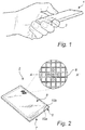
- Fig 1 schematically illustrates an application for a fingerprint sensing device according to an example embodiment of the present invention, in the form of a mobile phone 1 with an integrated fingerprint sensing device 2.
- the fingerprint sensing device 2 may, for example, be used for unlocking the mobile phone 1 and/or for authorizing transactions carried out using the mobile phone, etc.
- Fig 2 schematically shows the fingerprint sensing device 2 comprised in the mobile phone 1 in fig 1 .
- the fingerprint sensing device 2 comprises a sensor array 5, a power supply interface 6 and a communication interface 7.
- the sensor array 5 comprises a large number of sensing elements 8 (only one of the sensing elements has been indicated with a reference numeral to avoid cluttering the drawing), each being controllable to sense a distance between a sensing structure (top plate) comprised in the sensing element 8 and the surface of a finger contacting the top surface of the sensor array 5.
- a first sensing element is marked 'S' for sense and a second group of neighboring sensing elements are marked 'D' for drive.
- the power supply interface 6 comprises first 10a and second 10b contact pads, here shown as bond pads, for connection of a supply voltage V supply to the fingerprint sensor 2.
- the communication interface 7 comprises a number of bond pads for allowing control of the fingerprint sensor 2 and for acquisition of fingerprint data from the fingerprint sensor 2.
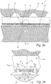
- Fig 3a is a schematic cross section of a portion of the fingerprint sensing device 2 in fig 2 taken along the line A-A' as indicated in fig 2 with a finger 11 placed on top of the sensor array 5.
- the fingerprint sensing device 2 comprises a doped semiconductor substrate 12, the plurality of sensing elements 8 formed on the semiconductor substrate 12, and a protective coating 13 on top of the sensing elements.
- the surface of the finger 11 comprises ridges 14 that are in contact with the protective coating 13 and valleys 15 that are spaced apart from the protective coating 13.
- each sensing element 8 comprises a sensing structure in the form of a sensing plate 17 adjacent to the protective coating 13. Below the sensing plate 17 are additional metal structures and active semiconductor circuitry schematically indicated by the hatched region 18 in fig 3a .
- Fig 3a is approximately drawn to scale to illustrate the relative dimensions of the protective coating 13, the sensing elements 8 and the ridges 14 and valleys 15 of the finger 11.
- the protective coating 13 is rather thick, in order to protect the sensing elements from wear and tear and ESD. Needless to say, the protective coating 13 is important for the robustness of the fingerprint sensing device 2. From the relative dimensions in fig 3a also follows that the capacitance between sensing structure 17 and finger 11 is very small, especially compared to parasitic capacitances between the sensing plate 17 and other conducting structures adjacent to the sensing plate 17. Examples of such conducting structures include neighboring sensing plates, the above-mentioned additional metal structures, the active semiconductor circuitry 18 and the substrate 12.
- the sensing element 8 comprises, in addition to the sensing plate 17, a shielding plate 20, a reference plate 21, and a charge amplifier 22.
- the charge amplifier 22 is, in fig 3b , only very schematically indicated by the dotted line.
- the only part of the charge amplifier 22 that is shown in some detail is the sense transistor (MOSFET) 23 to which the sensing plate 17 is connected. The reason for this type of illustration is to allow indication of the most important parasitic capacitances affecting the sensing element 8.
- C p3 also includes the internal capacitors in the sense transistor itself.
- the parasitic capacitance C p1 is in the order of 100 fF
- C p2 is in the order of 10 fF
- C p3 is in the order of 5-10 fF
- the finger capacitance C f to be sensed in in the order of 0.1 fF.
- Fig 4a is a hybrid of a partly structural and partly circuit schematic illustration of the sensing element 8 in figs 3a-b .
- the protective coating 13, the sensing plate 17, the shielding plate 20 and the reference plate 21 are schematically shown in an exploded perspective view, while the charge amplifier 22 is illustrated in the form of a transistor level circuit schematic.
- this first example of a simple charge amplifier 22 comprises sense transistor 23, cascode transistor 27, reset transistor 28 and bias current source 29.
- the sense transistor 23, the cascode transistor 27 and the reset transistor 28 are all formed in the same well 25.
- fig 4b the same schematic configuration is also shown in fig 4b , on a more abstract level with the transistor circuitry of fig 4a replaced by a general symbol for a charge amplifier having its negative input 30 connected to the sensing plate 17, its positive input 31 connected to excitation signal providing circuitry 32, here in the form of a pulse generator, and its output 33 providing a sensing signal V out indicative of the change in charge carried by the sensing plate 17 resulting from a change in a potential difference between the finger 11 and the sensing plate 17.
- the change in potential difference between the finger 11 and the sensing plate 17 results from the changing electric potential applied to the sensing plate 17 by the pulse generator 32 via the charge amplifier.
- a feedback capacitor formed by the sensing plate 17 and the reference plate 21, is connected between the negative input 30 and the output 33 of the charge amplifier 22. It should be noted that the general functionality of a charge amplifier is well known to one of ordinary skill in the relevant art. Fig 4b also schematically indicates that the well 25 is connected to the excitation signal providing circuitry 32.
- the gate of the sense transistor 23 constitutes the negative input 30 of the charge amplifier 22 and that the source of the sense transistor 23 constitutes the positive input 31 of the charge amplifier 22.
- the positive input 31 of the charge amplifier 22 is connected to the shielding plate 20, which is in turn connected to the well 25 in which the sense transistor 23 is formed, and to the pulse generator 32.
- the sensing element 8 further comprises a drive transistor 26, a drive control switch 35 and a reset control switch 36.
- the drive control switch 35 is controllable between a first state in which the gate of the drive transistor 26 is connected to the pulse generator 32 and a second state in which the gate of the drive transistor 26 is connected to ground.
- the drive control switch 35 When the drive control switch 35 is in its first state, the drive transistor 26 will be conducting and thus connect the sensing structure 17 directly to the pulse generator 32.
- the drive control switch is in its second state, the drive transistor 26 will be non-conducting. In the latter case, there will thus be no direct connection through the drive transistor 26 between the sensing structure 17 and the pulse generator 32.
- the drive transistor 26 is formed in the well 25.
- the bias current source 29 can be in the sensing element or outside the sensor array 5.
- the reset control switch 36 is controllable between a first state in which the reset transistor 28 is non-conducting to allow a potential difference between the sensing plate 17 and the feedback plate 21, and a second state in which the reset transistor 28 is conducting to equalize the potentials of the sensing plate 17 and the feedback plate 21.
- the sensing element 8 in fig 4a Through the configuration of the sensing element 8 in fig 4a , the influence of the internal parasitic capacitances C p1 and C p3 is removed or at least considerably reduced. Furthermore, driving neighboring sensing structures will remove or at least considerably reduce the influence of the parasitic capacitance C p2 between neighboring sensing plates 17 indicated in fig 3b . This can be achieved by either controlling neighboring sensing elements to be in their 'sense' state or in their 'drive' state, where the 'drive' state has the advantage of providing for a lower current consumption of the fingerprint sensing device 2.
- the present invention is not limited to the particular sensing element design of fig 4a , but that various elements of the sensing element can be realized in many different ways readily apparent to one of ordinary skill in the art based on the present disclosure.
- the charge amplifier may be provided in the form of a two-stage amplifier with differential inputs.
- FIG. 5 Another cross-section of a first implementation of the sensing element 8 in fig 4a is provided in fig 5 .
- the illustration in fig 5 mainly differs from that in fig 4a in that the physical transistor configuration of some of the transistors (the sense transistor 23 and the cascode transistor 27) comprised in the charge amplifier 22 is shown, while the relations in terms of electric potentials of various parts of the sensing element 8 (and neighboring sensing elements) are conceptually indicated using "bootstraps" 50, 51 and 52.
- fig 5 The main purpose of fig 5 is to show that the above-mentioned well 25 that is controlled to "follow" the potential of the sensing plate 17 is here an n-well that is formed in a p-doped substrate 12. Obviously, the well 25 may alternatively be a p-well that is formed in an n-doped substrate.
- Fig 6 is a similar drawing as fig 5 and schematically illustrates a second implementation of the sensing element 8 in fig 4a , which differs from what is shown in fig 6 in that the n-well 25 and a p-well 54 are both formed in an iso-well 55 that is in turn formed in the substrate 12 (which may be n-doped, p-doped or undoped).
- the iso-well 55, as well as the n-well 25 and the p-well 54 is controlled to follow the potential of the sensing plate 17, as is schematically illustrated by the additional "bootstraps" 53, 54. Specifically there can be potential differences between the wells.
- the iso-well 55 and the n-well 25 may be kept at the same potential, while the potential of the p-well 54 may follow the potential of the iso-well/n-well, but at a different (typically lower) potential
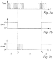
- fig 7a schematically shows the behavior potential of the well 25 (and of the sensing plate 17 with an offset)
- fig 7b schematically illustrates a state of the drive control switch 35
- fig 7c schematically illustrates a state of the reset control switch 36.
- the sensing element 8 is in its 'drive' state, at t 1 , the sensing element 8 is transitioned to its 'sense' state by operating the drive control switch 35, and at t 2 , the sensing element 8 is transitioned back to its 'drive' state by again operating the drive control switch to connect the sensing plate 17 to the pulse generator 32 through the drive transistor 26.
- the well 25 (and the sensing plate 17) exhibits a time varying potential that has substantially the same behavior in the 'sense' state and in the 'drive' state.
- the time-varying potential is applied to the sensing plate 17 through the drive transistor 26, and in the 'sense' state, the time-varying potential (possibly with an offset depending on the charge amplifier configuration) is applied to the sensing plate 17 via the charge amplifier 22.
- the reset control switch 36 is controlled to keep the reset transistor 28 non-conducting when the sensing element 8 is in its 'drive' state and alternating between conducting and non-conducting when the sensing element 8 is in its 'sense' state.
- An exemplary timing relation between the excitation signal applied to the sensing plate 17 during sensing and the operation of the reset transistor 27 will be described below with reference to figs 8a-c .
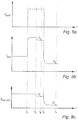
- Fig 8a is an enlarged portion of fig 7a
- fig 8b schematically shows a simulation of the sensing signal, that is, the signal at the output 33 of the charge amplifier 22 in fig 4a
- fig 8c schematically shows a simulated "corrected" version of the sensing signal that is referenced to a fixed reference potential (such as ground) rather than to the signal applied to the well 25 (which is the local reference potential for the charge amplifier 22 in fig 4a ).
- the excitation signal applied to the sensing plate 17 goes from low to high potential at t 3 , and then goes back from high to low at t 4 .
- the reset control switch 36 is operated to make the reset transistor 28 conducting, that is, connect the reference plate 21 to the sensing plate 17 through the reset transistor 28.
- the reset control switch 36 is again operated to make the reset transistor 28 non-conducting, that is, bring the charge amplifier in such a state that the output indicates a signal if the charge on the sensing plate 17 changes.
- the sensing signal is sampled a first time, resulting in a first sampled value S 1 .
- the excitation signal may be subtracted from the sensing signal present at the output 33 of the charge amplifier 22, resulting in corrected sampled voltages S 1 ' and S 2 '.
- the difference between S 2 ' and S 1 ' is a measure indicative of the capacitive coupling between the sensing plate 17 and the finger 11.
- the corrected signal of fig 8c or at least the corrected samples may be obtained in various ways, for instance through the use of an instrumentation amplifier or by using the excitation signal as a reference voltage for the sampling capacitors.
- a first step 101, the potentials of the sensing plate 17, the shielding plate 20, the well (n-well 25 in fig 6 or iso-well 54 in fig 7 ), and neighboring sensing plates are simultaneously changed from a first potential V 1 to a second potential V 2 (both of these potentials are referenced to a fixed potential, such as electrical ground).
- a sensing signal V out is provided, which is indicative of a change of a charge carried by the sensing plate 17 resulting from the change in the potential difference between the finger 11 and the sensing plate 17 resulting from the potential change in step 101.
Landscapes
- Engineering & Computer Science (AREA)
- Physics & Mathematics (AREA)
- General Physics & Mathematics (AREA)
- Health & Medical Sciences (AREA)
- Life Sciences & Earth Sciences (AREA)
- Human Computer Interaction (AREA)
- Multimedia (AREA)
- Theoretical Computer Science (AREA)
- Medical Informatics (AREA)
- Public Health (AREA)
- Biomedical Technology (AREA)
- Heart & Thoracic Surgery (AREA)
- Biophysics (AREA)
- Molecular Biology (AREA)
- Surgery (AREA)
- Animal Behavior & Ethology (AREA)
- General Health & Medical Sciences (AREA)
- Pathology (AREA)
- Veterinary Medicine (AREA)
- Computer Vision & Pattern Recognition (AREA)
- Quality & Reliability (AREA)
- Image Input (AREA)
- Measurement Of Length, Angles, Or The Like Using Electric Or Magnetic Means (AREA)
- Measurement Of The Respiration, Hearing Ability, Form, And Blood Characteristics Of Living Organisms (AREA)
- Transmission And Conversion Of Sensor Element Output (AREA)
Claims (14)
- Kapazitive Fingerabdruckfühlvorrichtung zum Fühlen eines Fingerabdruckmusters eines Fingers, wobei die Fingerabdruckfühlvorrichtung ein Halbleitersubstrat und eine Gruppierung von Fühlelementen umfasst, die auf dem Halbleitersubstrat gebildet sind,
wobei jedes der Fühlelemente umfasst:eine schützende dielektrische Deckschicht, die mit dem Finger in Berührung kommen soll;eine elektrisch leitfähige Fühlstruktur, die unter der Deckschicht angeordnet ist; undeinen Ladungsverstärker, der mit der Fühlstruktur verbunden ist, um ein Fühlsignal bereitzustellen, das eine Änderung einer durch die Fühlstruktur getragenen Ladung angibt, die aus einer Änderung in einer Potentialdifferenz zwischen dem Finger und der Fühlstruktur resultiert, wobei der Ladungsverstärker umfasst:einen negativen Eingang, der mit der Fühlstruktur verbunden ist;einen positiven Eingang;einen Ausgang, der das Fühlsignal bereitstellt;einen Rückmeldekondensator, der zwischen dem negativen Eingang und dem Ausgang angeschlossen ist; undeinen Fühltransistor mit einem Gate, welches den negativen Eingang bildet,wobei der Fühltransistor in einer Wanne (einem Well) in dem Halbleitersubstrat gebildet ist, wobei eine Grenzfläche zwischen dem Well und dem Substrat in einer solchen Weise ausgestaltet ist, dass das Fließen von Strom zwischen dem Well und dem Substrat verhindert werden kann; undwobei der Ladungsverstärker in einer solchen Weise ausgestaltet ist, dass ein Potential an dem negativen Eingang im Wesentlichen einem Potential an dem positiven Eingang folgt,wobei die Fingerabdruckfühlvorrichtung ferner umfasst:
Anregungssignal bereitstellende Schaltung(en), wobei die Anregungssignal bereitstellende(n) Schaltung(en) folgendes ist bzw. sind:Verbunden mit dem positiven Eingang und ausgestaltet, um ein Potential an dem positiven Eingang von einem ersten Potential zu einem zweiten Potential zu ändern, um dadurch ein Potential der Fühlstruktur zu ändern, wodurch die Änderung in der Potentialdifferenz zwischen dem Finger und der Fühlstruktur bereitgestellt wird; undVerbunden mit dem Well, um ein Potential des Wells von einem dritten Potential zu einem vierten Potential zu ändern, wobei eine Differenz zwischen dem dritten Potential und dem vierten Potential mindestens an Zeitpunkten, die für die Messung einer kapazitiven Kopplung zwischen der Fühlstruktur und dem Finger relevant sind, im Wesentlichen gleich einer Differenz zwischen dem ersten Potential und dem zweiten Potential ist, um dadurch einen Einfluss einer parasitären Kapazität zwischen der Fühlstruktur und dem Well zu reduzieren. - Fingerabdruckfühlvorrichtung nach Anspruch 1, ferner umfassend Abtastschaltung(en), die mit dem Ausgang des Ladungsverstärkers verbunden ist bzw. sind und ausgestaltet ist bzw. sind, um das Fühlsignal zu einer ersten Abtastzeit abzutasten, wenn der positive Eingang des Ladungsverstärkers auf dem ersten Potential gehalten wird und das Well auf dem dritten Potential gehalten wird, und zu einer zweiten Abtastzeit abzutasten, wenn der positive Eingang des Ladungsverstärkers auf dem zweiten Potential gehalten wird und das Well auf dem vierten Potential gehalten wird.
- Fingerabdruckfühlvorrichtung nach einem der vorhergehenden Ansprüche, wobei das dritte Potential im Wesentlichen gleich dem ersten Potential ist und das vierte Potential im Wesentlichen gleich dem zweiten Potential ist.
- Fingerabdruckfühlvorrichtung nach einem der vorhergehenden Ansprüche, wobei die Anregungssignal bereitstellende(n) Schaltung(en) einen Ausgang umfasst bzw. umfassen, der mit jedem von dem positiven Eingang und dem Well verbunden ist, um das Potential an dem positiven Eingang und das Potential des Wells simultan von dem ersten Potential zu dem zweiten Potential zu ändern.
- Fingerabdruckfühlvorrichtung nach einem der vorhergehenden Ansprüche, ferner umfassend eine Abschirmstruktur, die zwischen der Fühlstruktur und dem Substrat angeordnet ist,
wobei die Anregungssignal bereitstellende(n) Schaltung(en) ferner mit der Abschirmplatte verbunden und ausgestaltet ist bzw. sind, um ein Potential der Abschirmplatte von einem fünften Potential zu einem sechsten Potential zu ändern, und wobei das sechste Potential im Wesentlichen gleich einer Differenz zwischen dem ersten Potential und dem zweiten Potential ist. - Fingerabdruckfühlvorrichtung nach einem der vorhergehenden Ansprüche, wobei der Fühltransistor ein NMOS-Transistor oder ein PMOS-Transistor ist, und wobei das Well ein p-Well beziehungsweise ein n-Well ist.
- Fingerabdruckfühlvorrichtung nach einem der Ansprüche 1 bis 5, wobei mindestens eines von einem p-Well und einem n-Well in dem Well gebildet ist.
- Fingerabdruckfühlvorrichtung nach Anspruch 7, wobei ein gemeinsames Well für eine Vielzahl von Fühlelementen genutzt wird.
- Fingerabdruckfühlvorrichtung nach einem der vorhergehenden Ansprüche, wobei jedes der Fühlelemente ferner umfasst:einen Rücksetzschalter, der mindestens einen Rücksetztransistor umfasst, der zwischen dem negativen Eingang und dem Ausgang des Ladungsverstärkers angeschlossen ist und steuerbar ist, um den Rückmeldekondensator zu entladen,wobei der Rücksetztransistor in dem Well gebildet ist.
- Fingerabdruckfühlvorrichtung nach einem der vorhergehenden Ansprüche, wobei jedes der Fühlelemente ferner umfasst:Treibersignal bereitstellende Schaltung(en), die mindestens einen Treibertransistor umfasst bzw. umfassen, der mit der Fühlstruktur verbunden und steuerbar ist, um der Fühlstruktur direkt ein Treibersignal bereitzustellen,wobei der Treibertransistor in dem Well gebildet ist.
- Fingerabdruckfühlvorrichtung nach einem der vorhergehenden Ansprüche, ferner umfassend Ausleseschaltung(en), die mit jedem der Fühlelemente verbunden und ausgestaltet ist bzw. sind, um eine Darstellung des Fingerabdruckmusters bereitzustellen, die auf dem Fühlsignal von jedem der Fühlelemente basiert.
- Elektronische Vorrichtung, umfassend:die Fingerabdruckfühlvorrichtung gemäß Anspruch 11 undVerarbeitungsschaltung(en), die ausgestaltet ist bzw. sind zum:Erfassen der Darstellung des Fingerabdruckmusters von der Fingerabdruckfühlvorrichtung;Authentifizieren eines Benutzers basierend auf der Darstellung; undDurchführen von mindestens einem vom Benutzer angeforderten Verfahren nur dann, wenn der Benutzer basierend auf der Darstellung authentifiziert worden ist.
- Verfahren zum Fühlen eines Fingerabdruckmusters eines Fingers unter Verwendung einer Fingerabdruckfühlvorrichtung, die dotiertes Halbleitersubstrat und eine Gruppierung von Fühlelementen umfasst, die auf dem Halbleitersubstrat gebildet sind, wobei jedes der Fühlelemente eine elektrisch leitfähige Fühlstruktur einschließt, die mit dem Gate eines Fühltransistors verbunden ist, der in einem Well in dem Halbleitersubstrat gebildet worden ist, wobei das Well in Bezug auf das Halbleitersubstrat auf entgegengesetzte Polarität dotiert worden ist, wobei das Verfahren für jedes der Fühlelemente die Schritte umfasst:Ändern eines Potentials der Fühlstruktur von einem ersten Potential zu einem zweiten Potential;Ändern eines Potential des Wells von einem dritten Potential zu einem vierten Potential, wobei eine Differenz zwischen dem dritten Potential und dem vierten Potential mindestens an Zeitpunkten, die für die Messung einer kapazitiven Kopplung zwischen der Fühlstruktur und dem Finger relevant sind, im Wesentlichen gleich einer Differenz zwischen dem ersten Potential und dem zweiten Potential ist; undBereitstellen eines Fühlsignals, das eine Änderung einer von der Fühlstruktur getragenen Ladung angibt, die aus einer Änderung in einer Potentialdifferenz zwischen dem Finger und der Fühlstruktur resultiert, die durch die Änderung des Potentials der Fühlstruktur von dem ersten Potential zu dem zweiten Potential erreicht wird.
- Verfahren nach Anspruch 13, ferner umfassend den Schritt:
Ändern eines Potentials von jeder Fühlstruktur in einer Vielzahl benachbarter Fühlelemente von einem siebten Potential zu einem achten Potential, wobei eine Differenz zwischen dem siebten Potential und dem achten Potential im Wesentlichen gleich einer Differenz zwischen dem ersten Potential und dem zweiten Potential ist.
Applications Claiming Priority (2)
| Application Number | Priority Date | Filing Date | Title |
|---|---|---|---|
| SE1450336 | 2014-03-24 | ||
| PCT/SE2015/050331 WO2015147727A1 (en) | 2014-03-24 | 2015-03-20 | Capacitive fingerprint sensor with improved sensing element |
Publications (3)
| Publication Number | Publication Date |
|---|---|
| EP3123395A1 EP3123395A1 (de) | 2017-02-01 |
| EP3123395A4 EP3123395A4 (de) | 2017-11-29 |
| EP3123395B1 true EP3123395B1 (de) | 2019-10-16 |
Family
ID=54196074
Family Applications (1)
| Application Number | Title | Priority Date | Filing Date |
|---|---|---|---|
| EP15768075.2A Active EP3123395B1 (de) | 2014-03-24 | 2015-03-20 | Kapazitiver fingerabdruckfühler mit verbessertem sensorelement |
Country Status (7)
| Country | Link |
|---|---|
| US (1) | US9152841B1 (de) |
| EP (1) | EP3123395B1 (de) |
| JP (2) | JP6495937B2 (de) |
| KR (1) | KR101773031B1 (de) |
| CN (2) | CN107346412B (de) |
| TW (1) | TWI520074B (de) |
| WO (1) | WO2015147727A1 (de) |
Families Citing this family (55)
| Publication number | Priority date | Publication date | Assignee | Title |
|---|---|---|---|---|
| US8485442B2 (en) | 2009-07-02 | 2013-07-16 | Biometric Payment Solutions | Electronic transaction verification system with biometric authentication |
| US9852322B2 (en) * | 2012-05-04 | 2017-12-26 | Apple Inc. | Finger biometric sensing device including series coupled error compensation and drive signal nulling circuitry and related methods |
| SE1351489A1 (sv) * | 2013-12-12 | 2015-06-13 | Fingerprint Cards Ab | Fingeravtrycksavkänningssystem och -metod |
| US9489559B2 (en) * | 2014-05-28 | 2016-11-08 | Fingerprint Cards Ab | Electronic device with fingerprint sensing system and conducting housing |
| US9519819B2 (en) | 2014-07-14 | 2016-12-13 | Fingerprint Cards Ab | Method and electronic device for noise mitigation |
| CN104331202A (zh) | 2014-11-07 | 2015-02-04 | 深圳市汇顶科技股份有限公司 | 指纹检测电路、传感器和触摸屏 |
| US20160171276A1 (en) * | 2014-12-11 | 2016-06-16 | Elan Microelectronics Corporation | Fingerprint Sensor Having ESD Protection Structure |
| US9460576B2 (en) * | 2014-12-22 | 2016-10-04 | Fingerprint Cards Ab | Capacitive fingerprint sensing device with demodulation circuitry in sensing element |
| US9600705B2 (en) * | 2015-02-11 | 2017-03-21 | Fingerprint Cards Ab | Capacitive fingerprint sensing device with current readout from sensing elements |
| TW201638756A (zh) * | 2015-04-21 | 2016-11-01 | 映智科技股份有限公司 | 感測裝置 |
| KR102002081B1 (ko) * | 2015-06-19 | 2019-07-22 | 크루셜텍 (주) | 지문 검출 장치 및 이의 구동 방법 |
| US9880688B2 (en) | 2015-08-05 | 2018-01-30 | Synaptics Incorporated | Active matrix capacitive sensor for common-mode cancellation |
| US9684812B2 (en) * | 2015-09-29 | 2017-06-20 | Fingerprint Cards Ab | Fingerprint sensing device with common mode suppression |
| CN105335715A (zh) * | 2015-10-28 | 2016-02-17 | 深圳市汇顶科技股份有限公司 | 指纹识别系统 |
| US10282585B2 (en) | 2015-11-13 | 2019-05-07 | Cypress Semiconductor Corporation | Sensor-compatible overlay |
| US10832029B2 (en) | 2015-11-13 | 2020-11-10 | Cypress Semiconductor Corporation | Sensor-compatible overlay |
| US9639734B1 (en) | 2015-11-13 | 2017-05-02 | Cypress Semiconductor Corporation | Fingerprint sensor-compatible overlay material |
| US9600707B1 (en) * | 2015-11-30 | 2017-03-21 | Fingerprint Cards Ab | Analog sampling system and method for noise supression |
| CN105335737B (zh) * | 2015-12-02 | 2019-03-15 | 苏州迈瑞微电子有限公司 | 电容指纹传感器 |
| KR20170102668A (ko) | 2016-03-02 | 2017-09-12 | 삼성전자주식회사 | 지문 감지 센서, 이를 포함하는 전자 장치 및 지문 감지 센서의 동작 방법 |
| SE539638C2 (en) | 2016-04-22 | 2017-10-24 | Fingerprint Cards Ab | Fingerprint sensing system with adaptive power control |
| SE1650548A1 (en) * | 2016-04-22 | 2017-10-23 | Fingerprint Cards Ab | Fingerprint sensing system with sensing reference potential providing circuitry |
| TWI719203B (zh) * | 2016-05-13 | 2021-02-21 | 瑞典商指紋卡公司 | 用於雜訊偵測的指紋感測裝置及其中的方法 |
| SE539668C2 (en) * | 2016-06-01 | 2017-10-24 | Fingerprint Cards Ab | Fingerprint sensing device and method for manufacturing a fingerprint sensing device |
| WO2018035759A1 (zh) * | 2016-08-24 | 2018-03-01 | 深圳市汇顶科技股份有限公司 | 电容判读电路及指纹辨识系统 |
| US10121046B2 (en) | 2016-08-31 | 2018-11-06 | Himax Technologies Limited | Dermatoglyph identification apparatus and identifying method thereof |
| TWI630561B (zh) * | 2016-09-02 | 2018-07-21 | 奇景光電股份有限公司 | 皮紋辨識裝置及其辨識方法 |
| CN107808112B (zh) * | 2016-09-09 | 2020-03-24 | 奇景光电股份有限公司 | 皮纹识别装置及其识别方法 |
| KR101763589B1 (ko) * | 2016-09-29 | 2017-08-01 | (주)세미센스 | 정전용량방식 센서장치 |
| CN107918682A (zh) * | 2016-10-08 | 2018-04-17 | 深圳指瑞威科技有限公司 | 基于Ansoft Maxwell的手指电容建模的方法 |
| CN107918749A (zh) * | 2016-10-08 | 2018-04-17 | 深圳指瑞威科技有限公司 | 基于bcd工艺的高穿透能力的指纹传感器 |
| US10430634B2 (en) * | 2016-10-11 | 2019-10-01 | Innolux Corporation | Biometric sensing device and display device |
| KR102028267B1 (ko) * | 2016-10-27 | 2019-10-02 | 선전 구딕스 테크놀로지 컴퍼니, 리미티드 | 정전용량식 지문 센서 |
| US10102412B2 (en) * | 2016-11-17 | 2018-10-16 | Fingerprint Cards Ab | Fingerprint sensing with different capacitive configurations |
| US9922231B1 (en) * | 2016-11-17 | 2018-03-20 | Fingerprint Cards Ab | Fingerprint sensing with voltage pattern configurations |
| US9946920B1 (en) * | 2016-11-23 | 2018-04-17 | Image Match Design Inc. | Sensing element and fingerprint sensor comprising the sensing elements |
| US10078776B2 (en) | 2016-12-16 | 2018-09-18 | Sunasic Technologies Inc. | Noise reduced capacitive fingerprint sensor and capacitive sensing unit included therein |
| US10216972B2 (en) * | 2017-01-13 | 2019-02-26 | Synaptics Incorporated | Pixel architecture and driving scheme for biometric sensing |
| KR102703414B1 (ko) * | 2017-01-25 | 2024-09-09 | 삼성디스플레이 주식회사 | 차량용 표시 장치 및 이를 포함하는 차량 제어 시스템 |
| EP3358496B1 (de) | 2017-02-02 | 2021-04-07 | Nxp B.V. | Vorrichtung und verfahren zur verarbeitung von fingerabdrücken |
| TWI626596B (zh) * | 2017-02-14 | 2018-06-11 | 宏碁股份有限公司 | 指紋感測裝置、電子裝置以及指紋感測器的校準方法 |
| CN108985150B (zh) | 2017-05-31 | 2022-05-27 | 联咏科技股份有限公司 | 电容式图像传感器 |
| ES2895657T3 (es) * | 2017-12-21 | 2022-02-22 | Fingerprint Cards Ab | Dispositivo de detección de huellas dactilares con estructura de compensación de bordes. |
| CN108780503B (zh) * | 2018-02-12 | 2022-05-03 | 深圳市汇顶科技股份有限公司 | 指纹检测电路、指纹识别装置以及终端设备 |
| TWI652625B (zh) * | 2018-03-16 | 2019-03-01 | 友達光電股份有限公司 | 指紋感測裝置 |
| US10679034B2 (en) * | 2018-06-08 | 2020-06-09 | Synaptics Incorporated | Short latency fingerprint sensing |
| US11015914B2 (en) * | 2019-01-21 | 2021-05-25 | Novatek Microelectronics Corp. | Capacitive image sensing device and capacitive image sensing method |
| CN111353406B (zh) * | 2020-02-24 | 2023-04-07 | 成都高迈微电子有限公司 | 一种无激励信号无boost芯片的指纹传感器采集单元 |
| JP7205702B2 (ja) * | 2020-09-18 | 2023-01-17 | 速博思股▲ふん▼有限公司 | 指紋認識装置 |
| EP4049044B1 (de) | 2020-11-05 | 2024-05-01 | Fingerprint Cards Anacatum IP AB | Verfahren und system zur auswertung von fingerabdrucksensoren |
| SE2051294A1 (en) * | 2020-11-06 | 2022-05-07 | Fingerprint Cards Anacatum Ip Ab | Integrated biometric sensor module and method for manufacturing a smartcard comprising an integrated biometric sensor module |
| CN112560640B (zh) * | 2020-12-08 | 2024-07-26 | 京东方科技集团股份有限公司 | 指纹采集电路、驱动方法、指纹传感器及指纹采集设备 |
| KR102365146B1 (ko) * | 2021-02-13 | 2022-02-23 | 이성호 | 기생용량을 개조한 쉴딩용량을 이용하여 감도를 향상시키는 방법 |
| EP4505426A1 (de) * | 2022-04-08 | 2025-02-12 | Fingerprint Cards Anacatum IP AB | Fingerabdrucksensor mit ladungsveränderungsanordnung |
| CN115988859B (zh) * | 2022-09-09 | 2026-03-10 | 湖北长江新型显示产业创新中心有限公司 | 一种显示模组和显示装置 |
Family Cites Families (35)
| Publication number | Priority date | Publication date | Assignee | Title |
|---|---|---|---|---|
| US6320394B1 (en) * | 1996-02-14 | 2001-11-20 | Stmicroelectronics S.R.L. | Capacitive distance sensor |
| US6483931B2 (en) * | 1997-09-11 | 2002-11-19 | Stmicroelectronics, Inc. | Electrostatic discharge protection of a capacitve type fingerprint sensing array |
| DE19836770C1 (de) * | 1998-08-13 | 2000-04-20 | Siemens Ag | Verfahren zur kapazitiven Bilderfassung |
| JP2000213908A (ja) * | 1998-11-16 | 2000-08-04 | Sony Corp | 静電容量検出装置およびその検査方法並びに指紋照合装置 |
| DE60032286T8 (de) * | 1999-06-10 | 2007-09-27 | Nippon Telegraph And Telephone Corp. | Gerät zur Erkennung von Oberflächengestalten |
| WO2001006448A1 (en) * | 1999-07-14 | 2001-01-25 | Veridicom, Inc. | Ultra-rugged i.c. sensor and method of making the same |
| DE10101081B4 (de) * | 2001-01-11 | 2007-06-06 | Infineon Technologies Ag | Schottky-Diode |
| JP2003028607A (ja) * | 2001-07-12 | 2003-01-29 | Sony Corp | 静電容量検出装置およびこれを用いた指紋照合装置 |
| JP2003078365A (ja) * | 2001-09-05 | 2003-03-14 | Sony Corp | オペアンプ回路、静電容量検出装置および指紋照合装置 |
| JP4035418B2 (ja) * | 2001-10-31 | 2008-01-23 | 株式会社本田電子技研 | 近接スイッチおよび物体検出装置 |
| US6636053B1 (en) * | 2001-11-02 | 2003-10-21 | Stmicroelectronics, Inc. | Capacitive pixel for fingerprint sensor |
| US6927581B2 (en) * | 2001-11-27 | 2005-08-09 | Upek, Inc. | Sensing element arrangement for a fingerprint sensor |
| FI115109B (fi) * | 2003-01-22 | 2005-02-28 | Nokia Corp | Tunnistusjärjestely ja tunnistusjärjestelyn käsittävä matkaviestin |
| CN1310180C (zh) * | 2003-05-06 | 2007-04-11 | 祥群科技股份有限公司 | 一种电容式指纹感测器及其制造方法 |
| JP3741282B2 (ja) * | 2003-07-28 | 2006-02-01 | セイコーエプソン株式会社 | 入力装置、電子機器及び入力装置の駆動方法 |
| KR100564915B1 (ko) * | 2004-02-10 | 2006-03-30 | 한국과학기술원 | 정전용량방식 지문센서 및 이를 이용한 지문 센싱방법 |
| JP2005326167A (ja) * | 2004-05-12 | 2005-11-24 | Alps Electric Co Ltd | 容量検出型センサ |
| EP1766547B1 (de) | 2004-06-18 | 2008-11-19 | Fingerprint Cards AB | Fingerabdruck-sensor-element |
| US7606399B2 (en) * | 2004-07-23 | 2009-10-20 | Nippon Telegraph And Telephone Corporation | Surface shape recognizing sensor device |
| KR100672619B1 (ko) * | 2005-05-16 | 2007-01-24 | 주식회사 유니온커뮤니티 | 지문영상 강화를 위한 정전용량방식 지문센서 |
| JP5098276B2 (ja) * | 2006-09-29 | 2012-12-12 | 富士通セミコンダクター株式会社 | 半導体装置の製造方法 |
| JP2008244021A (ja) * | 2007-03-26 | 2008-10-09 | Matsushita Electric Ind Co Ltd | 固体撮像装置およびそれを用いたカメラ |
| CN101373752B (zh) * | 2007-08-20 | 2011-01-26 | 神盾股份有限公司 | 具软性电路板信号传输结构的指纹感测芯片及其制造方法 |
| US7548051B1 (en) * | 2008-02-21 | 2009-06-16 | Mediatek Inc. | Low drop out voltage regulator |
| US8005276B2 (en) * | 2008-04-04 | 2011-08-23 | Validity Sensors, Inc. | Apparatus and method for reducing parasitic capacitive coupling and noise in fingerprint sensing circuits |
| JP4710929B2 (ja) * | 2008-06-06 | 2011-06-29 | カシオ計算機株式会社 | 接触検知装置及びその検知方法 |
| TWI379244B (en) * | 2008-10-08 | 2012-12-11 | Egis Technology Inc | Imaging device |
| CN101727575B (zh) * | 2008-10-22 | 2012-09-05 | 神盾股份有限公司 | 图像感测装置 |
| JP2011215124A (ja) * | 2010-03-15 | 2011-10-27 | Alps Electric Co Ltd | 容量検出装置及び容量検出方法 |
| WO2012048263A1 (en) * | 2010-10-08 | 2012-04-12 | Authentec, Inc. | Finger sensing device including differential measurement circuitry and related methods |
| JP2013217824A (ja) * | 2012-04-11 | 2013-10-24 | Seiko Epson Corp | テラヘルツカメラ及び電子機器 |
| US9740343B2 (en) | 2012-04-13 | 2017-08-22 | Apple Inc. | Capacitive sensing array modulation |
| US9372582B2 (en) * | 2012-04-19 | 2016-06-21 | Atmel Corporation | Self-capacitance measurement |
| US9581628B2 (en) | 2012-05-04 | 2017-02-28 | Apple Inc. | Electronic device including device ground coupled finger coupling electrode and array shielding electrode and related methods |
| US9390307B2 (en) | 2012-05-04 | 2016-07-12 | Apple Inc. | Finger biometric sensing device including error compensation circuitry and related methods |
-
2014
- 2014-11-20 US US14/548,834 patent/US9152841B1/en active Active
-
2015
- 2015-03-09 TW TW104107383A patent/TWI520074B/zh not_active IP Right Cessation
- 2015-03-20 CN CN201710339666.3A patent/CN107346412B/zh active Active
- 2015-03-20 CN CN201580002035.1A patent/CN105593878B/zh active Active
- 2015-03-20 KR KR1020167022016A patent/KR101773031B1/ko active Active
- 2015-03-20 JP JP2016558559A patent/JP6495937B2/ja active Active
- 2015-03-20 WO PCT/SE2015/050331 patent/WO2015147727A1/en not_active Ceased
- 2015-03-20 EP EP15768075.2A patent/EP3123395B1/de active Active
-
2019
- 2019-03-07 JP JP2019041376A patent/JP6750059B2/ja active Active
Non-Patent Citations (1)
| Title |
|---|
| None * |
Also Published As
| Publication number | Publication date |
|---|---|
| JP6495937B2 (ja) | 2019-04-03 |
| JP2017510897A (ja) | 2017-04-13 |
| KR101773031B1 (ko) | 2017-08-30 |
| CN107346412A (zh) | 2017-11-14 |
| US9152841B1 (en) | 2015-10-06 |
| EP3123395A1 (de) | 2017-02-01 |
| CN107346412B (zh) | 2022-01-11 |
| JP2019144251A (ja) | 2019-08-29 |
| WO2015147727A1 (en) | 2015-10-01 |
| EP3123395A4 (de) | 2017-11-29 |
| US20150310248A1 (en) | 2015-10-29 |
| KR20160135172A (ko) | 2016-11-25 |
| TWI520074B (zh) | 2016-02-01 |
| JP6750059B2 (ja) | 2020-09-02 |
| TW201537467A (zh) | 2015-10-01 |
| CN105593878B (zh) | 2017-06-13 |
| CN105593878A (zh) | 2016-05-18 |
Similar Documents
| Publication | Publication Date | Title |
|---|---|---|
| EP3123395B1 (de) | Kapazitiver fingerabdruckfühler mit verbessertem sensorelement | |
| US9600705B2 (en) | Capacitive fingerprint sensing device with current readout from sensing elements | |
| US9672401B2 (en) | Fingerprint sensing system and method | |
| EP3356996B1 (de) | Fingerabdruckerfassende vorrichtung mit gleichtaktunterdrückung | |
| US9489559B2 (en) | Electronic device with fingerprint sensing system and conducting housing | |
| CN110476170B (zh) | 具有边缘补偿结构的指纹感测装置 | |
| US9710690B1 (en) | Fingerprint sensing system with adaptive power control |
Legal Events
| Date | Code | Title | Description |
|---|---|---|---|
| STAA | Information on the status of an ep patent application or granted ep patent |
Free format text: STATUS: THE INTERNATIONAL PUBLICATION HAS BEEN MADE |
|
| PUAI | Public reference made under article 153(3) epc to a published international application that has entered the european phase |
Free format text: ORIGINAL CODE: 0009012 |
|
| STAA | Information on the status of an ep patent application or granted ep patent |
Free format text: STATUS: REQUEST FOR EXAMINATION WAS MADE |
|
| 17P | Request for examination filed |
Effective date: 20160913 |
|
| AK | Designated contracting states |
Kind code of ref document: A1 Designated state(s): AL AT BE BG CH CY CZ DE DK EE ES FI FR GB GR HR HU IE IS IT LI LT LU LV MC MK MT NL NO PL PT RO RS SE SI SK SM TR |
|
| AX | Request for extension of the european patent |
Extension state: BA ME |
|
| DAV | Request for validation of the european patent (deleted) | ||
| DAX | Request for extension of the european patent (deleted) | ||
| A4 | Supplementary search report drawn up and despatched |
Effective date: 20171103 |
|
| RIC1 | Information provided on ipc code assigned before grant |
Ipc: G06K 9/00 20060101AFI20171026BHEP Ipc: H03K 17/96 20060101ALI20171026BHEP Ipc: A61B 5/117 20160101ALI20171026BHEP Ipc: G01R 27/26 20060101ALI20171026BHEP |
|
| GRAP | Despatch of communication of intention to grant a patent |
Free format text: ORIGINAL CODE: EPIDOSNIGR1 |
|
| STAA | Information on the status of an ep patent application or granted ep patent |
Free format text: STATUS: GRANT OF PATENT IS INTENDED |
|
| INTG | Intention to grant announced |
Effective date: 20190522 |
|
| GRAS | Grant fee paid |
Free format text: ORIGINAL CODE: EPIDOSNIGR3 |
|
| GRAA | (expected) grant |
Free format text: ORIGINAL CODE: 0009210 |
|
| STAA | Information on the status of an ep patent application or granted ep patent |
Free format text: STATUS: THE PATENT HAS BEEN GRANTED |
|
| AK | Designated contracting states |
Kind code of ref document: B1 Designated state(s): AL AT BE BG CH CY CZ DE DK EE ES FI FR GB GR HR HU IE IS IT LI LT LU LV MC MK MT NL NO PL PT RO RS SE SI SK SM TR |
|
| REG | Reference to a national code |
Ref country code: GB Ref legal event code: FG4D |
|
| REG | Reference to a national code |
Ref country code: CH Ref legal event code: EP |
|
| REG | Reference to a national code |
Ref country code: DE Ref legal event code: R096 Ref document number: 602015039942 Country of ref document: DE |
|
| REG | Reference to a national code |
Ref country code: IE Ref legal event code: FG4D |
|
| REG | Reference to a national code |
Ref country code: AT Ref legal event code: REF Ref document number: 1192001 Country of ref document: AT Kind code of ref document: T Effective date: 20191115 |
|
| REG | Reference to a national code |
Ref country code: NL Ref legal event code: MP Effective date: 20191016 |
|
| REG | Reference to a national code |
Ref country code: LT Ref legal event code: MG4D |
|
| REG | Reference to a national code |
Ref country code: AT Ref legal event code: MK05 Ref document number: 1192001 Country of ref document: AT Kind code of ref document: T Effective date: 20191016 |
|
| PG25 | Lapsed in a contracting state [announced via postgrant information from national office to epo] |
Ref country code: SE Free format text: LAPSE BECAUSE OF FAILURE TO SUBMIT A TRANSLATION OF THE DESCRIPTION OR TO PAY THE FEE WITHIN THE PRESCRIBED TIME-LIMIT Effective date: 20191016 Ref country code: LV Free format text: LAPSE BECAUSE OF FAILURE TO SUBMIT A TRANSLATION OF THE DESCRIPTION OR TO PAY THE FEE WITHIN THE PRESCRIBED TIME-LIMIT Effective date: 20191016 Ref country code: PL Free format text: LAPSE BECAUSE OF FAILURE TO SUBMIT A TRANSLATION OF THE DESCRIPTION OR TO PAY THE FEE WITHIN THE PRESCRIBED TIME-LIMIT Effective date: 20191016 Ref country code: NO Free format text: LAPSE BECAUSE OF FAILURE TO SUBMIT A TRANSLATION OF THE DESCRIPTION OR TO PAY THE FEE WITHIN THE PRESCRIBED TIME-LIMIT Effective date: 20200116 Ref country code: GR Free format text: LAPSE BECAUSE OF FAILURE TO SUBMIT A TRANSLATION OF THE DESCRIPTION OR TO PAY THE FEE WITHIN THE PRESCRIBED TIME-LIMIT Effective date: 20200117 Ref country code: LT Free format text: LAPSE BECAUSE OF FAILURE TO SUBMIT A TRANSLATION OF THE DESCRIPTION OR TO PAY THE FEE WITHIN THE PRESCRIBED TIME-LIMIT Effective date: 20191016 Ref country code: PT Free format text: LAPSE BECAUSE OF FAILURE TO SUBMIT A TRANSLATION OF THE DESCRIPTION OR TO PAY THE FEE WITHIN THE PRESCRIBED TIME-LIMIT Effective date: 20200217 Ref country code: FI Free format text: LAPSE BECAUSE OF FAILURE TO SUBMIT A TRANSLATION OF THE DESCRIPTION OR TO PAY THE FEE WITHIN THE PRESCRIBED TIME-LIMIT Effective date: 20191016 Ref country code: BG Free format text: LAPSE BECAUSE OF FAILURE TO SUBMIT A TRANSLATION OF THE DESCRIPTION OR TO PAY THE FEE WITHIN THE PRESCRIBED TIME-LIMIT Effective date: 20200116 Ref country code: NL Free format text: LAPSE BECAUSE OF FAILURE TO SUBMIT A TRANSLATION OF THE DESCRIPTION OR TO PAY THE FEE WITHIN THE PRESCRIBED TIME-LIMIT Effective date: 20191016 Ref country code: AT Free format text: LAPSE BECAUSE OF FAILURE TO SUBMIT A TRANSLATION OF THE DESCRIPTION OR TO PAY THE FEE WITHIN THE PRESCRIBED TIME-LIMIT Effective date: 20191016 |
|
| PG25 | Lapsed in a contracting state [announced via postgrant information from national office to epo] |
Ref country code: RS Free format text: LAPSE BECAUSE OF FAILURE TO SUBMIT A TRANSLATION OF THE DESCRIPTION OR TO PAY THE FEE WITHIN THE PRESCRIBED TIME-LIMIT Effective date: 20191016 Ref country code: IS Free format text: LAPSE BECAUSE OF FAILURE TO SUBMIT A TRANSLATION OF THE DESCRIPTION OR TO PAY THE FEE WITHIN THE PRESCRIBED TIME-LIMIT Effective date: 20200224 Ref country code: HR Free format text: LAPSE BECAUSE OF FAILURE TO SUBMIT A TRANSLATION OF THE DESCRIPTION OR TO PAY THE FEE WITHIN THE PRESCRIBED TIME-LIMIT Effective date: 20191016 |
|
| PG25 | Lapsed in a contracting state [announced via postgrant information from national office to epo] |
Ref country code: AL Free format text: LAPSE BECAUSE OF FAILURE TO SUBMIT A TRANSLATION OF THE DESCRIPTION OR TO PAY THE FEE WITHIN THE PRESCRIBED TIME-LIMIT Effective date: 20191016 |
|
| REG | Reference to a national code |
Ref country code: DE Ref legal event code: R097 Ref document number: 602015039942 Country of ref document: DE |
|
| PG2D | Information on lapse in contracting state deleted |
Ref country code: IS |
|
| PG25 | Lapsed in a contracting state [announced via postgrant information from national office to epo] |
Ref country code: RO Free format text: LAPSE BECAUSE OF FAILURE TO SUBMIT A TRANSLATION OF THE DESCRIPTION OR TO PAY THE FEE WITHIN THE PRESCRIBED TIME-LIMIT Effective date: 20191016 Ref country code: EE Free format text: LAPSE BECAUSE OF FAILURE TO SUBMIT A TRANSLATION OF THE DESCRIPTION OR TO PAY THE FEE WITHIN THE PRESCRIBED TIME-LIMIT Effective date: 20191016 Ref country code: DK Free format text: LAPSE BECAUSE OF FAILURE TO SUBMIT A TRANSLATION OF THE DESCRIPTION OR TO PAY THE FEE WITHIN THE PRESCRIBED TIME-LIMIT Effective date: 20191016 Ref country code: ES Free format text: LAPSE BECAUSE OF FAILURE TO SUBMIT A TRANSLATION OF THE DESCRIPTION OR TO PAY THE FEE WITHIN THE PRESCRIBED TIME-LIMIT Effective date: 20191016 Ref country code: CZ Free format text: LAPSE BECAUSE OF FAILURE TO SUBMIT A TRANSLATION OF THE DESCRIPTION OR TO PAY THE FEE WITHIN THE PRESCRIBED TIME-LIMIT Effective date: 20191016 Ref country code: IS Free format text: LAPSE BECAUSE OF FAILURE TO SUBMIT A TRANSLATION OF THE DESCRIPTION OR TO PAY THE FEE WITHIN THE PRESCRIBED TIME-LIMIT Effective date: 20200216 |
|
| PLBE | No opposition filed within time limit |
Free format text: ORIGINAL CODE: 0009261 |
|
| STAA | Information on the status of an ep patent application or granted ep patent |
Free format text: STATUS: NO OPPOSITION FILED WITHIN TIME LIMIT |
|
| PG25 | Lapsed in a contracting state [announced via postgrant information from national office to epo] |
Ref country code: SM Free format text: LAPSE BECAUSE OF FAILURE TO SUBMIT A TRANSLATION OF THE DESCRIPTION OR TO PAY THE FEE WITHIN THE PRESCRIBED TIME-LIMIT Effective date: 20191016 Ref country code: SK Free format text: LAPSE BECAUSE OF FAILURE TO SUBMIT A TRANSLATION OF THE DESCRIPTION OR TO PAY THE FEE WITHIN THE PRESCRIBED TIME-LIMIT Effective date: 20191016 Ref country code: IT Free format text: LAPSE BECAUSE OF FAILURE TO SUBMIT A TRANSLATION OF THE DESCRIPTION OR TO PAY THE FEE WITHIN THE PRESCRIBED TIME-LIMIT Effective date: 20191016 |
|
| 26N | No opposition filed |
Effective date: 20200717 |
|
| PG25 | Lapsed in a contracting state [announced via postgrant information from national office to epo] |
Ref country code: MC Free format text: LAPSE BECAUSE OF FAILURE TO SUBMIT A TRANSLATION OF THE DESCRIPTION OR TO PAY THE FEE WITHIN THE PRESCRIBED TIME-LIMIT Effective date: 20191016 |
|
| REG | Reference to a national code |
Ref country code: CH Ref legal event code: PL |
|
| PG25 | Lapsed in a contracting state [announced via postgrant information from national office to epo] |
Ref country code: SI Free format text: LAPSE BECAUSE OF FAILURE TO SUBMIT A TRANSLATION OF THE DESCRIPTION OR TO PAY THE FEE WITHIN THE PRESCRIBED TIME-LIMIT Effective date: 20191016 |
|
| REG | Reference to a national code |
Ref country code: BE Ref legal event code: MM Effective date: 20200331 |
|
| PG25 | Lapsed in a contracting state [announced via postgrant information from national office to epo] |
Ref country code: LU Free format text: LAPSE BECAUSE OF NON-PAYMENT OF DUE FEES Effective date: 20200320 |
|
| PG25 | Lapsed in a contracting state [announced via postgrant information from national office to epo] |
Ref country code: LI Free format text: LAPSE BECAUSE OF NON-PAYMENT OF DUE FEES Effective date: 20200331 Ref country code: CH Free format text: LAPSE BECAUSE OF NON-PAYMENT OF DUE FEES Effective date: 20200331 Ref country code: IE Free format text: LAPSE BECAUSE OF NON-PAYMENT OF DUE FEES Effective date: 20200320 |
|
| PG25 | Lapsed in a contracting state [announced via postgrant information from national office to epo] |
Ref country code: BE Free format text: LAPSE BECAUSE OF NON-PAYMENT OF DUE FEES Effective date: 20200331 |
|
| REG | Reference to a national code |
Ref country code: DE Ref legal event code: R079 Ref document number: 602015039942 Country of ref document: DE Free format text: PREVIOUS MAIN CLASS: G06K0009000000 Ipc: G06V0010000000 |
|
| REG | Reference to a national code |
Ref country code: DE Ref legal event code: R081 Ref document number: 602015039942 Country of ref document: DE Owner name: FINGERPRINT CARDS ANACATUM IP AB, SE Free format text: FORMER OWNER: FINGERPRINT CARDS AB, GOETEBORG, SE |
|
| REG | Reference to a national code |
Ref country code: GB Ref legal event code: 732E Free format text: REGISTERED BETWEEN 20220310 AND 20220316 |
|
| PG25 | Lapsed in a contracting state [announced via postgrant information from national office to epo] |
Ref country code: TR Free format text: LAPSE BECAUSE OF FAILURE TO SUBMIT A TRANSLATION OF THE DESCRIPTION OR TO PAY THE FEE WITHIN THE PRESCRIBED TIME-LIMIT Effective date: 20191016 Ref country code: MT Free format text: LAPSE BECAUSE OF FAILURE TO SUBMIT A TRANSLATION OF THE DESCRIPTION OR TO PAY THE FEE WITHIN THE PRESCRIBED TIME-LIMIT Effective date: 20191016 Ref country code: CY Free format text: LAPSE BECAUSE OF FAILURE TO SUBMIT A TRANSLATION OF THE DESCRIPTION OR TO PAY THE FEE WITHIN THE PRESCRIBED TIME-LIMIT Effective date: 20191016 |
|
| PG25 | Lapsed in a contracting state [announced via postgrant information from national office to epo] |
Ref country code: MK Free format text: LAPSE BECAUSE OF FAILURE TO SUBMIT A TRANSLATION OF THE DESCRIPTION OR TO PAY THE FEE WITHIN THE PRESCRIBED TIME-LIMIT Effective date: 20191016 |
|
| PGFP | Annual fee paid to national office [announced via postgrant information from national office to epo] |
Ref country code: GB Payment date: 20260327 Year of fee payment: 12 |
|
| PGFP | Annual fee paid to national office [announced via postgrant information from national office to epo] |
Ref country code: DE Payment date: 20260327 Year of fee payment: 12 |
|
| PGFP | Annual fee paid to national office [announced via postgrant information from national office to epo] |
Ref country code: FR Payment date: 20260325 Year of fee payment: 12 |