EP3124989A1 - Détecteur de champs magnétique à trois axes à puce unique et son procédé de préparation - Google Patents
Détecteur de champs magnétique à trois axes à puce unique et son procédé de préparation Download PDFInfo
- Publication number
- EP3124989A1 EP3124989A1 EP15768352.5A EP15768352A EP3124989A1 EP 3124989 A1 EP3124989 A1 EP 3124989A1 EP 15768352 A EP15768352 A EP 15768352A EP 3124989 A1 EP3124989 A1 EP 3124989A1
- Authority
- EP
- European Patent Office
- Prior art keywords
- axis
- sensor
- axis sensor
- magnetic field
- magnetoresistive
- Prior art date
- Legal status (The legal status is an assumption and is not a legal conclusion. Google has not performed a legal analysis and makes no representation as to the accuracy of the status listed.)
- Granted
Links
Images




Classifications
-
- G—PHYSICS
- G01—MEASURING; TESTING
- G01R—MEASURING ELECTRIC VARIABLES; MEASURING MAGNETIC VARIABLES
- G01R33/00—Arrangements or instruments for measuring magnetic variables
- G01R33/0011—Arrangements or instruments for measuring magnetic variables comprising means, e.g. flux concentrators, flux guides, for guiding or concentrating the magnetic flux, e.g. to the magnetic sensor
-
- G—PHYSICS
- G01—MEASURING; TESTING
- G01R—MEASURING ELECTRIC VARIABLES; MEASURING MAGNETIC VARIABLES
- G01R3/00—Apparatus or processes specially adapted for the manufacture or maintenance of measuring instruments, e.g. of probe tips
-
- G—PHYSICS
- G01—MEASURING; TESTING
- G01R—MEASURING ELECTRIC VARIABLES; MEASURING MAGNETIC VARIABLES
- G01R33/00—Arrangements or instruments for measuring magnetic variables
- G01R33/0052—Manufacturing aspects; Manufacturing of single devices, i.e. of semiconductor magnetic sensor chips
-
- G—PHYSICS
- G01—MEASURING; TESTING
- G01R—MEASURING ELECTRIC VARIABLES; MEASURING MAGNETIC VARIABLES
- G01R33/00—Arrangements or instruments for measuring magnetic variables
- G01R33/02—Measuring direction or magnitude of magnetic fields or magnetic flux
- G01R33/0206—Three-component magnetometers
-
- G—PHYSICS
- G01—MEASURING; TESTING
- G01R—MEASURING ELECTRIC VARIABLES; MEASURING MAGNETIC VARIABLES
- G01R33/00—Arrangements or instruments for measuring magnetic variables
- G01R33/02—Measuring direction or magnitude of magnetic fields or magnetic flux
- G01R33/06—Measuring direction or magnitude of magnetic fields or magnetic flux using galvano-magnetic devices
- G01R33/09—Magnetoresistive devices
-
- H—ELECTRICITY
- H10—SEMICONDUCTOR DEVICES; ELECTRIC SOLID-STATE DEVICES NOT OTHERWISE PROVIDED FOR
- H10N—ELECTRIC SOLID-STATE DEVICES NOT OTHERWISE PROVIDED FOR
- H10N50/00—Galvanomagnetic devices
- H10N50/01—Manufacture or treatment
-
- H—ELECTRICITY
- H10—SEMICONDUCTOR DEVICES; ELECTRIC SOLID-STATE DEVICES NOT OTHERWISE PROVIDED FOR
- H10N—ELECTRIC SOLID-STATE DEVICES NOT OTHERWISE PROVIDED FOR
- H10N50/00—Galvanomagnetic devices
- H10N50/10—Magnetoresistive devices
Definitions
- the present invention relates to the field of magnetic field sensors, and in particular to a monolithic three-axis magnetic field sensor and its manufacturing method.
- magnetic field sensors have developed from early single-axis magnetic field sensors to later double-axis magnetic field sensors and then to current three-axis magnetic field sensors, such that they can detect magnetic field signals in three directions of X, Y and Z axes in the space comprehensively.
- magnetic field sensors such as AMR, GMR and TMR
- a magnetic field sensing direction is in a film plane, and measurement on X-axis and Y-axis magnetic field components in the plane may be implemented by making two sensors orthogonal, thereby implementing an XY two-axis magnetic field test system.
- Another solution is using a slope to set a magnetic field sensor unit to detect a magnetic signal in the Z direction, as disclosed in the patent CN202548308U entitled "Three-Axis Magnetic Field Sensor".
- an angle of forming the slope in the sensor in this structure is hard to control, and shadowing effects are likely to be caused in the process of depositing a magnetoresistive film on the slope, thereby reducing the performance of a magnetic field sensor element.
- an algorithm is needed to calculate a magnetic signal in the Z-axis direction.
- Another solution is a solution disclosed in the patent application 201310202801.1 entitled "A Three-Axis Digital Compass", which converts a Z-axis magnetic field component perpendicular to a plane into a magnetic field component in an XY plane by using a distortion function of a flux concentrator on the magnetic field, thereby implementing measurement on a magnetic signal in a Z-axis direction.
- the magnetic field sensor in this structure needs an ASIC chip or computation using an algorithm to obtain magnetic signals in three directions of the X, Y and Z axes.
- a three-axis magnetic field sensor is manufactured mainly by methods such as etching a substrate layer of a substrate to form a slope, depositing a magnetoresistive material film on the slope and double deposition, for example, a manufacturing process of a sensor disclosed in the patent CN202548308U entitled "Three-Axis Magnetic Field Sensor” substantially comprises etching a substrate layer of a wafer to form two slopes, double-depositing a magnetoresistive material film on the two slopes respectively, and conducting double annealing to manufacture sensor units in an XZ direction and a YZ direction.
- the European Patent Application EP 2267470 B1 also discloses a method for manufacturing a three-axis sensor, in which a substrate is etched to form a slope, and a sensor unit for measuring a magnetic field component in a Z-axis direction is manufactured on the slope.
- Grades of the etched slopes in the two patent applications are hard to control, and there is difficulty in depositing the magnetoresistive material film on the slope, which are not conducive to actual implementation.
- the present invention provides a monolithic three-axis magnetic field sensor and its manufacturing method.
- the monolithic three-axis magnetic field sensor can directly output magnetic signals in three directions of X, Y and Z without the need to conduct computation with an algorithm.
- the manufacture thereof does not need grooving to form a slope, and the three-axis magnetic field sensor can be obtained directly by double deposition, in which an X-axis sensor and a Y-axis sensor are perpendicular to each other, and magnetization directions of pinned layers of magnetoresistive sensing element comprised therein are also perpendicular to each other.
- the magnetoresistive sensing element is a GMR spin valve element or a TMR sensing element.
- the magnetic flux guide is an array of rectangular strips, the length thereof in a direction perpendicular to the magnetization direction of the pinned layer of the magnetoresistive sensing element being greater than the length thereof along the magnetization direction of the pinned layer of the magnetoresistive sensing element, and is made of soft ferromagnetic alloy.
- the numbers of the magnetoresistive sensing elements on the respective sensing arms and reference arms of the X-axis sensor and the Y-axis sensor are the same; and the numbers of the magnetoresistive sensing elements on the push arm and the pull arm of the push-pull bridge of the Z-axis sensor are the same.
- the length of the magnetoresistive sensing element in a direction perpendicular to the magnetization direction of the pinned layer is greater than the length thereof along the magnetization direction of the pinned layer.
- a gap S between the adjacent two of the magnetic flux guides of the Z-axis sensor is not less than the minimum one of three-dimensional sizes of the magnetic flux guide of the Z-axis sensor.
- the magnetoresistive sensing elements achieve magnetization direction of the magnetic free layer perpendicular to that of the pinned layer by permanent magnet bias, double-exchange interaction, shape anisotropy or any combination thereof.
- the reference bridge and the push-pull bridge are both of a half-bridge, full-bridge or quasi-bridge structure.
- the substrate is integrated with an ASIC chip thereon, or the substrate is electrically connected to a separate ASIC chip.
- the monolithic three-axis magnetic field sensor further comprises at least 3 bonding pads, or the X-axis sensor, the Y-axis sensor and the Z-axis sensor each have at least 3 through silicon vias.
- the present invention further provides a method for manufacturing a monolithic three-axis linear magnetic field sensor, the method comprising:
- the semiconductor wafer is a silicon wafer doped with an integrated circuit, a silicon wafer subjected to chemico-mechanical polishing, or a blank silicon wafer comprising a passivated smooth surface.
- FIG. 1 is a schematic structural diagram of a monolithic three-axis magnetic field sensor in the present invention in an XY plane.
- the sensor comprises a substrate 1, the substrate 1 is integrated with an X-axis sensor 3, a Y-axis sensor 4, a Z-axis sensor 5 and a plurality of bonding pads 2 for input and output, wherein, the X-axis sensor 3 and the Y-axis sensor 4 have identical structures but different arrangement directions, and they are perpendicular to each other.
- the X-axis sensor 3 and the Y-axis sensor 4 have identical structures but different arrangement directions, and they are perpendicular to each other.
- elements in the X-axis sensor 3 are arranged longitudinally, and elements in the Y-axis sensor 4 are arranged transversely; however, elements in the X-axis sensor 3 may also be arranged transversely, and at this point, elements in the Y-axis sensor 4 are arranged longitudinally.
- the X-axis sensor 3 comprises sensing element series 11, reference element series 12 and an X-magnetic flux guide 8, and the Y-axis sensor 4 comprises sensing element series 13, reference element series 14 and a Y-magnetic flux guide 9, wherein the reference element series 12, 14 are respectively placed beneath the X-magnetic flux guide 8 and the Y-magnetic flux guide 9, the sensing element series 11, 13 are respectively placed at a gap between two adjacent X-magnetic flux guides 8 and a gap between two adjacent Y-magnetic flux guides, and the sensing element series 11, 13 and the reference element series 12, 14 are each formed by electrically connecting one or more identical magnetoresistive sensing elements.
- the Z-axis sensor comprises a Z-magnetic flux guide 10, and magnetoresistive sensing elements 15, 16, wherein the magnetoresistive sensing elements 15, 16 are electrically connected in columns respectively and arranged at two sides at the bottom of the Z-magnetic flux guide 10.
- magnetoresistive sensing elements forming the reference element series 12, 14 may also be placed above the X-magnetic flux guide 8 and the Y-magnetic flux guide 9 respectively, and at this point, the magnetoresistive sensing elements 15, 16 in the Z-axis sensor are placed at two sides at the top of the Z-magnetic flux guide 10.
- All the magnetoresistive sensing elements are GMR spin valves or TMR sensing elements, and may be, but not limited to, square-shaped, rhombic-shaped, or oval-shaped.
- Magnetization directions 6 of pinned layers of the magnetoresistive sensing elements in the X-axis sensor 3 and the Z-axis sensor 5 are the same, and are both along an X-axis direction, but magnetization directions 6 and 7 of pinned layers of the magnetoresistive sensing elements in the X-axis sensor 3 and the Y-axis sensor 4 are perpendicular to each other.
- the magnetoresistive sensing elements When there is no external magnetic field, the magnetoresistive sensing elements achieve magnetization direction of the magnetic free layer perpendicular to that of the pinned layer by permanent magnet bias, double-exchange interaction, shape anisotropy or any combination thereof.
- All the magnetic flux guides are each an array of rectangular strips, the length thereof in a direction perpendicular to the magnetization direction of the pinned layer of the magnetoresistive sensing element being greater than the length thereof along the magnetization direction of the pinned layer of the magnetoresistive sensing element, and are made of soft ferromagnetic alloy, wherein the alloy may include, but not limited to, one or more elements including Ni, Fe, Co, Si, B, Ni, Zr and Al.
- the bonding pads 2 comprise input/output connection bonding pads in the X-axis sensor 3, the Y-axis sensor 4 and the Z-axis sensor 5.
- the substrate 1 may comprise an ASIC, or may be electrically connected to an additional separate ASIC chip, and the ASIC is not shown in the drawing.
- the monolithic three-axis linear magnetic field sensor is packaged by using wire bonding of bonding pads, and may also be packaged by using technologies such as through silicon via, flip-chip, ball grid array (BGA) package, wafer level package (WLP), and chip on board (COB).
- FIG. 2 is a schematic diagram of a digital signal processing circuit of a monolithic three-axis linear magnetic field sensor. Magnetic signals sensed by the X-axis sensor 3, the Y-axis sensor 4 and the Z-axis sensor 5 are analog-to-digital converted by using an ADC 41 in a digital signal processing circuit 50, converted digital signals are transmitted to a data processor 42, and processed signals are output by an I/O, thereby implementing measurement on an external magnetic field.
- the digital signal processing circuit 50 may be placed on the substrate 1, or placed on another ASIC chip, the ASIC chip being electrically connected to the substrate 1.
- FIG. 3 is a schematic structural diagram of the X-axis sensor in FIG. 1 .
- the X-axis sensor is of a reference full-bridge structure, and comprises a reference arm and a sensing arm.
- the reference arm comprises a plurality of reference element series 12 placed beneath the X-magnetic flux guide, and the sensing arm comprises a plurality of sensing element series 11 placed at gaps 9 of the X-magnetic flux guides.
- the sensing element series 11 and the reference element series are mutually staggered, and arranged along a long axis direction of the X-magnetic flux guide, wherein each one of the reference element series 12 is adjacent to at least one of the sensing element series 11, and each one of the sensing element series 11 is also adjacent to at least one of the reference element series 12.
- Each one of the sensing element series 11 is spaced from the adjacent one of the reference element series 12 by an interval L, and the interval L is very small, preferably 20-100 microns.
- the sensing arm, the reference arm and the bonding pads 17-20 may be connected by an electrical connection conductor 21.
- the bonding pads 17-20 are each used as an input end Vbias, a ground end GND, and output ends V1, V2, corresponding to the leftmost four bonding pads in FIG. 1 .
- FIG. 4 shows distribution of magnetic fields around the sensing element series 11 and the reference element series 12 in FIG. 3 . It can be seen from the drawing that the magnitude of the magnetic field sensed by the sensing element series 11 at the gap of the X-magnetic flux guide 8 is increased, and the magnitude of the magnetic field sensed by the reference element series 12 placed beneath the X-magnetic flux guide 8 is reduced, and it is thus clear that the X-magnetic flux guide 8 can play a role of attenuating magnetic fields.
- FIG. 6 is a relation curve of an output voltage of the X-axis sensor in FIG. 3 vs. the external magnetic field. It can be seen from the drawing that the X-axis sensor can only sense a magnetic field component in an X-axis direction, the output voltage Vx36 does not respond to magnetic field components in a Y-axis direction and a Z-axis direction; voltages Vy37 and Vz38 are both zero, and Vx36 is symmetric about the origin 0.
- FIG. 7 is a schematic circuit diagram of the X-axis sensor in FIG. 3 .
- two sensing arms 52, 52' and two reference arms 53, 53' are connected at an interval to construct a full-bridge, and an output voltage of the full-bridge is
- the sensitivity of the X-axis sensor may be expressed as:
- the Y-axis sensor 4 is of a structure identical to that of the X-axis sensor 3, and therefore, a working principle, surrounding magnetic field distribution, and a response curve thereof are all identical to those of the X-axis sensor 3, which are not repeated herein.
- FIG. 8 is a schematic structural diagram of a Z-axis sensor.
- the Z-axis sensor is of a push-pull full-bridge structure.
- the Z-axis sensor comprises a plurality of magnetoresistive sensing elements 15 and 16, a plurality of Z-magnetic flux guides 10, an electrical connection conductor 27, and bonding pads 28-30, wherein the bonding pads 28-30 are each used as a power supply end V Bias , a ground end GND, and voltage output ends V+, V-, corresponding to the rightmost four bonding pads in the bonding pads 2 in FIG. 1 .
- All the magnetoresistive sensing elements 15 are electrically connected to each other to form a push arm of the full-bridge, and all the magnetoresistive sensing elements 16 are electrically connected to each other to form a pull arm of the full-bridge.
- the push arm is arranged to be spaced from the pull arm, and the push arm, the pull arm and the bonding pads 28-30 are connected through the electrical connection conductor 27 to form the push-pull full-bridge.
- the magnetoresistive sensing elements 15, 16 are arranged along the length direction of the Z-magnetic flux guides 10. In FIG. 8 , the magnetoresistive sensing elements 15, 16 are arranged at two sides at the bottom of the Z-magnetic flux guide 10 in rows, and are covered by the Z-magnetic flux guide 10.
- a row of push arm magnetoresistive sensing elements 15 and a row of pull arm magnetoresistive sensing elements 16 are arranged at two sides at the bottom of each Z-magnetic flux guide 10, and if necessary, the magnetoresistive sensing elements 15, 16 may also be arranged beneath the three Z- magnetic flux guides 10.
- FIG. 9 is a diagram of magnetic field distribution of the Z-axis sensor in an external magnetic field 106 in the Z-axis direction. It can be seen from the distribution of magnetic force lines in the drawing that the external magnetic field is distorted near the Z-magnetic flux guide 10, thereby generating the magnetic field component in the X-axis direction, and the magnetoresistive sensing elements 15 and 16 beneath the Z-magnetic flux guide 10 can just detect this component; however, directions of the magnetic field components detected by them are opposite to each other, and are 107 and 108 respectively.
- the magnitude of the applied external magnetic field can be known through the detected X-axis magnetic field component.
- FIG. 10 is a schematic circuit diagram of the Z-axis sensor.
- Several magnetoresistive sensing elements 15 are electrically connected to form equivalent magnetoresistors R2 and R2', several magnetoresistive sensing elements 16 are electrically connected to form two equivalent magnetoresistors R3 and R3', and the four magnetoresistors are connected to construct a full-bridge.
- changing situations of resistances of the magnetoresistors R2, R2' and R3, R3' may be opposite to each other, thereby constructing a push-pull output.
- V out V Bias R 2 ⁇ R 3 R 2 + R 3
- FIG. 11 is a diagram of magnetic field distribution of the Z-axis sensor in an external magnetic field 100 in the X-axis direction. It can be seen from the drawing that magnetic fields detected by the magnetoresistive sensing elements 15 and 16 are the same, this may result in that changing situations of resistances of the magnetoresistors R2, R2' and R3, R3' are the same, such that no push-pull output is formed, and therefore, the sensor will not respond.
- FIG. 12 is a diagram of magnetic field distribution of the Z-axis sensor in an external magnetic field 101 in the Y-axis direction. It can be seen from the drawing that the Z- magnetic flux guide 10 completely shields the external magnetic field in the Y-axis direction, and the magnetoresistive sensing elements 15, 16 are insensitive to the magnetic field in the Y-axis direction; therefore, the magnetoresistive sensing elements 15, 16 do not detect any magnetic field component, and the Z-axis sensor does not respond either.
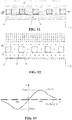
- FIG. 13 is a relation curve of an output voltage of the Z-axis sensor vs. an external magnetic field. It can be seen from the drawing that the Z-axis sensor can only sense the magnetic component in the Z-axis direction, the output voltage Vz38 does not respond to magnetic field components in the X-axis and Y-axis directions, voltages Vx36 and Vy37 are both 0, and Vz38 is symmetric about the origin 0.
- FIG. 14 is a process flow for manufacturing a monolithic three-axis magnetic field sensor in the present invention, and the method for manufacturing the sensor comprises the following steps:
- FIG. 16 a schematic sectional diagram of a single monolithic three-axis sensor is shown in FIG. 16 , and a schematic diagram of structural arrangement of all the three-axis sensors on a wafer is shown in FIG. 17 .
- the wafer in the above steps may be a silicon wafer doped with an integrated circuit, a silicon wafer subjected to chemico-mechanical polishing, or a blank silicon wafer comprising a passivated smooth surface, and the wafer may further comprise coils.
- antiferromagnetic materials on the pinned layers in the first magnetoresistive material film stack and the second magnetoresistive material film stack are different, the structure of the first magnetoresistive material film stack is PtMn/SAF/tunnel barrier/free layer/IrMn, the structure of the second magnetoresistive material film stack is IrMn/SAF/tunnel barrier/free layer/PtMn, and the two stack structures are also interchangeable.
- the blocking temperature TB1 of PtMn is higher than the blocking temperature TB2 of IrMn, and in this way, the films used for constructing the X-axis sensor and the Y-axis sensor may be annealed in the same step, and magnetization directions of a bias layer and the pinned layer may also be crossed at the same time.
- the double-step annealing conducted in the step (2) refers to first conducting annealing in a high-temperature magnetic field at the temperature higher than TB1, at this point, an applied magnetic field being along the X-axis direction, and then conducting annealing in a low-temperature magnetic field at the temperature between TB1 and TB2, at this point, a direction of a magnetic field applied to the wafer being perpendicular to the direction of the high-temperature magnetic field.
Landscapes
- Physics & Mathematics (AREA)
- General Physics & Mathematics (AREA)
- Condensed Matter Physics & Semiconductors (AREA)
- Engineering & Computer Science (AREA)
- Manufacturing & Machinery (AREA)
- Measuring Magnetic Variables (AREA)
- Hall/Mr Elements (AREA)
Applications Claiming Priority (2)
| Application Number | Priority Date | Filing Date | Title |
|---|---|---|---|
| CN201410123285.8A CN103913709B (zh) | 2014-03-28 | 2014-03-28 | 一种单芯片三轴磁场传感器及其制备方法 |
| PCT/CN2015/075146 WO2015144073A1 (fr) | 2014-03-28 | 2015-03-26 | Détecteur de champs magnétique à trois axes à puce unique et son procédé de préparation |
Publications (3)
| Publication Number | Publication Date |
|---|---|
| EP3124989A1 true EP3124989A1 (fr) | 2017-02-01 |
| EP3124989A4 EP3124989A4 (fr) | 2017-12-06 |
| EP3124989B1 EP3124989B1 (fr) | 2019-05-29 |
Family
ID=51039536
Family Applications (1)
| Application Number | Title | Priority Date | Filing Date |
|---|---|---|---|
| EP15768352.5A Active EP3124989B1 (fr) | 2014-03-28 | 2015-03-26 | Détecteur de champs magnétique à trois axes monolithique et son procédé de fabrication |
Country Status (5)
| Country | Link |
|---|---|
| US (1) | US10107871B2 (fr) |
| EP (1) | EP3124989B1 (fr) |
| JP (1) | JP6496005B2 (fr) |
| CN (1) | CN103913709B (fr) |
| WO (1) | WO2015144073A1 (fr) |
Cited By (6)
| Publication number | Priority date | Publication date | Assignee | Title |
|---|---|---|---|---|
| EP3199966A4 (fr) * | 2014-09-28 | 2018-07-25 | Multidimension Technology Co., Ltd. | Pont de capteurs de champ magnétique symétrique à couche libre de différentiel à puce unique et procédé de préparation |
| EP3244226A4 (fr) * | 2015-01-07 | 2018-09-12 | Multidimension Technology Co., Ltd. | Capteur à magnéto-résistance linéaire dans l'axe z comprenant une puce unique et une bobine d'étalonnage/de réinitialisation |
| EP3502724A1 (fr) * | 2017-12-15 | 2019-06-26 | Biosense Webster (Israel) Ltd. | Capteur de tas amélioré |
| EP3617727A4 (fr) * | 2017-04-26 | 2021-05-05 | Multidimension Technology Co., Ltd. | Capteur magnétorésistif à faible bruit ayant une structure de modulation magnétique multicouche |
| WO2023217356A1 (fr) * | 2022-05-10 | 2023-11-16 | Sensitec Gmbh | Capteur vectoriel de champ magnétique et son procédé de fabrication |
| CN113777384B (zh) * | 2021-09-28 | 2023-12-12 | 南方电网数字电网研究院有限公司 | 四分裂导线电流检测方法、装置、计算机设备和存储介质 |
Families Citing this family (45)
| Publication number | Priority date | Publication date | Assignee | Title |
|---|---|---|---|---|
| CN103913709B (zh) * | 2014-03-28 | 2017-05-17 | 江苏多维科技有限公司 | 一种单芯片三轴磁场传感器及其制备方法 |
| CN103954920B (zh) | 2014-04-17 | 2016-09-14 | 江苏多维科技有限公司 | 一种单芯片三轴线性磁传感器及其制备方法 |
| CN103995240B (zh) * | 2014-05-30 | 2017-11-10 | 江苏多维科技有限公司 | 一种磁电阻z轴梯度传感器芯片 |
| CN104197828B (zh) * | 2014-08-20 | 2017-07-07 | 江苏多维科技有限公司 | 一种单芯片偏轴磁电阻z‑x角度传感器和测量仪 |
| CN104698409B (zh) * | 2015-02-04 | 2017-11-10 | 江苏多维科技有限公司 | 一种单芯片具有校准线圈/重置线圈的高强度磁场x轴线性磁电阻传感器 |
| US10405995B2 (en) | 2015-03-12 | 2019-09-10 | Korea Works' Compensation & Welfare Service | Artificial limb structure having magnetic lock device |
| CN104776794B (zh) * | 2015-04-16 | 2017-11-10 | 江苏多维科技有限公司 | 一种单封装的高强度磁场磁电阻角度传感器 |
| CN105044631B (zh) * | 2015-08-28 | 2018-08-07 | 江苏多维科技有限公司 | 一种半翻转两轴线性磁电阻传感器 |
| CN105259518A (zh) * | 2015-11-03 | 2016-01-20 | 江苏多维科技有限公司 | 一种高灵敏度单芯片推挽式tmr磁场传感器 |
| CN105389014A (zh) * | 2015-12-17 | 2016-03-09 | 安徽寰智信息科技股份有限公司 | 一种三维人机交互系统 |
| CN105371845A (zh) * | 2015-12-17 | 2016-03-02 | 安徽寰智信息科技股份有限公司 | 一种惯性追踪模块 |
| JP6724459B2 (ja) * | 2016-03-23 | 2020-07-15 | Tdk株式会社 | 磁気センサ |
| US10067201B2 (en) * | 2016-04-14 | 2018-09-04 | Texas Instruments Incorporated | Wiring layout to reduce magnetic field |
| US10184991B2 (en) * | 2016-05-11 | 2019-01-22 | Texas Instruments Incorporated | Dual-axis fluxgate device |
| CN107479010B (zh) * | 2016-06-07 | 2019-06-04 | 江苏多维科技有限公司 | 一种具有补偿线圈的磁电阻传感器 |
| JP6240994B1 (ja) * | 2016-12-15 | 2017-12-06 | 朝日インテック株式会社 | 3次元磁界検出素子および3次元磁界検出装置 |
| WO2018199068A1 (fr) * | 2017-04-25 | 2018-11-01 | コニカミノルタ株式会社 | Capteur magnétique |
| TWI665460B (zh) * | 2017-07-17 | 2019-07-11 | 愛盛科技股份有限公司 | 磁場感測元件以及磁場感測裝置 |
| JP6699635B2 (ja) * | 2017-08-18 | 2020-05-27 | Tdk株式会社 | 磁気センサ |
| US11237231B2 (en) | 2017-12-26 | 2022-02-01 | Robert Bosch Gmbh | Z-axis magnetic sensor with distributed flux guides |
| CN111615636B (zh) * | 2018-01-17 | 2022-07-08 | 阿尔卑斯阿尔派株式会社 | 磁检测装置及其制造方法 |
| WO2019142635A1 (fr) * | 2018-01-17 | 2019-07-25 | アルプスアルパイン株式会社 | Dispositif de détection magnétique et son procédé de fabrication |
| CN108413992A (zh) * | 2018-01-30 | 2018-08-17 | 江苏多维科技有限公司 | 一种三轴预调制低噪声磁电阻传感器 |
| JP6538226B1 (ja) * | 2018-03-23 | 2019-07-03 | Tdk株式会社 | 磁気センサ |
| JP6620834B2 (ja) * | 2018-03-27 | 2019-12-18 | Tdk株式会社 | 磁気センサおよび磁気センサシステム |
| US11579209B2 (en) * | 2018-06-22 | 2023-02-14 | Zhenghong Qian | Three-axis magnetic sensor |
| CN109522649B (zh) * | 2018-11-16 | 2023-03-14 | 西安电子科技大学 | 基于正交试验的硅通孔tsv阵列温度优化方法 |
| CN110297194B (zh) * | 2019-07-24 | 2022-02-18 | 江西联创光电科技股份有限公司 | 一种支持三维气隙磁场测量的传感器的安装方法和设备 |
| CN112305470B (zh) * | 2019-07-29 | 2022-12-06 | 甘肃省科学院传感技术研究所 | 由磁化方向不同的巨磁阻结构构建的巨磁阻传感器的退火方法 |
| JP7375419B2 (ja) * | 2019-09-26 | 2023-11-08 | Tdk株式会社 | 磁気センサ |
| CN111277231B (zh) * | 2020-02-18 | 2022-02-18 | 江苏多维科技有限公司 | 一种增益可控的磁阻模拟放大器 |
| US10775450B1 (en) | 2020-03-28 | 2020-09-15 | QuSpin, Inc. | Zero field parametric resonance magnetometer with triaxial sensitivity |
| CN111596239B (zh) * | 2020-06-15 | 2021-07-20 | 北京航空航天大学 | 一种单片集成三轴隧穿磁电阻的磁传感器及其制备方法 |
| US11275130B2 (en) * | 2020-06-25 | 2022-03-15 | Western Digital Technologies, Inc. | Magnetic sensor bridge using dual free layer |
| WO2022067599A1 (fr) * | 2020-09-30 | 2022-04-07 | 上海灿瑞科技股份有限公司 | Magnétomètre à effet hall à trois axes |
| CN114252817B (zh) * | 2021-12-16 | 2023-04-11 | 北京微纳星空科技有限公司 | 一种高精度磁通门探头及其制作方法 |
| CN115394582B (zh) * | 2022-08-24 | 2026-04-24 | Oppo广东移动通信有限公司 | 非接触式开关及电子设备 |
| CN115728681B (zh) * | 2022-11-15 | 2023-09-12 | 南方电网数字电网研究院有限公司 | 磁场传感器及其测试方法、装置、制备方法和计算机设备 |
| CN115825826B (zh) * | 2022-12-22 | 2023-09-15 | 南方电网数字电网研究院有限公司 | 一种三轴全桥电路变换式线性磁场传感器 |
| CN116299082B (zh) * | 2023-03-02 | 2026-03-27 | 北京芯可鉴科技有限公司 | 3d混叠结构的三维磁场传感器及其制备方法 |
| CN116106801B (zh) * | 2023-04-14 | 2023-06-20 | 珠海多创科技有限公司 | 磁阻传感器、磁传感装置及其制备方法 |
| CN117075008B (zh) * | 2023-08-01 | 2025-01-14 | 江苏多维科技有限公司 | 多轴磁场传感器以及多轴磁场传感器芯片 |
| CN117075007B (zh) * | 2023-08-01 | 2024-10-29 | 江苏多维科技有限公司 | Z轴磁场传感器及其加工制备方法 |
| CN116859298B (zh) * | 2023-08-01 | 2025-01-14 | 江苏多维科技有限公司 | 多轴磁场传感器 |
| CN117630772B (zh) * | 2023-10-12 | 2025-08-01 | 北京智芯微电子科技有限公司 | 三维隧道磁阻传感器及其制造方法 |
Family Cites Families (22)
| Publication number | Priority date | Publication date | Assignee | Title |
|---|---|---|---|---|
| US7054114B2 (en) * | 2002-11-15 | 2006-05-30 | Nve Corporation | Two-axis magnetic field sensor |
| US7126330B2 (en) | 2004-06-03 | 2006-10-24 | Honeywell International, Inc. | Integrated three-dimensional magnetic sensing device and method to fabricate an integrated three-dimensional magnetic sensing device |
| JP4614061B2 (ja) * | 2004-09-28 | 2011-01-19 | ヤマハ株式会社 | 巨大磁気抵抗効果素子を用いた磁気センサ及び同磁気センサの製造方法 |
| US7687284B2 (en) * | 2005-01-13 | 2010-03-30 | Yamaha Corporation | Magnetic sensor and manufacturing method therefor |
| EP1860450B1 (fr) * | 2005-03-17 | 2011-06-08 | Yamaha Corporation | Capteur magnetique et son procede de fabrication |
| CN100593122C (zh) * | 2005-12-09 | 2010-03-03 | 中国科学院物理研究所 | 一种平面集成的三维磁场传感器及其制备方法和用途 |
| JP4296180B2 (ja) * | 2006-02-17 | 2009-07-15 | 株式会社東芝 | 磁気抵抗効果素子,磁気ヘッド,磁気再生装置,および磁気抵抗素子の製造方法 |
| JP2009175120A (ja) * | 2007-12-28 | 2009-08-06 | Alps Electric Co Ltd | 磁気センサ及び磁気センサモジュール |
| US20090315554A1 (en) * | 2008-06-20 | 2009-12-24 | Honeywell International Inc. | Integrated three-dimensional magnetic sensing device and method to fabricate an integrated three-dimensional magnetic sensing device |
| CN101599522B (zh) * | 2009-06-30 | 2011-05-25 | 厦门市三安光电科技有限公司 | 一种采用绝缘介质阻挡层的垂直发光二极管及其制备方法 |
| US8390283B2 (en) * | 2009-09-25 | 2013-03-05 | Everspin Technologies, Inc. | Three axis magnetic field sensor |
| JP5297442B2 (ja) * | 2010-12-15 | 2013-09-25 | アルプス電気株式会社 | 磁気センサ |
| CN102810630B (zh) * | 2011-05-30 | 2015-11-25 | 中国科学院物理研究所 | 各向异性可调制的磁性薄膜结构、磁敏传感器及制备方法 |
| CN102426344B (zh) * | 2011-08-30 | 2013-08-21 | 江苏多维科技有限公司 | 三轴磁场传感器 |
| US9000760B2 (en) * | 2012-02-27 | 2015-04-07 | Everspin Technologies, Inc. | Apparatus and method for resetting a Z-axis sensor flux guide |
| CN202548308U (zh) | 2012-04-23 | 2012-11-21 | 美新半导体(无锡)有限公司 | 三轴磁传感器 |
| CN103267520B (zh) | 2013-05-21 | 2016-09-14 | 江苏多维科技有限公司 | 一种三轴数字指南针 |
| CN103267955B (zh) * | 2013-05-28 | 2016-07-27 | 江苏多维科技有限公司 | 单芯片桥式磁场传感器 |
| CN103412269B (zh) * | 2013-07-30 | 2016-01-20 | 江苏多维科技有限公司 | 单芯片推挽桥式磁场传感器 |
| CN203480009U (zh) * | 2013-09-10 | 2014-03-12 | 江苏多维科技有限公司 | 一种单芯片z轴线性磁电阻传感器 |
| CN103913709B (zh) | 2014-03-28 | 2017-05-17 | 江苏多维科技有限公司 | 一种单芯片三轴磁场传感器及其制备方法 |
| CN203811786U (zh) * | 2014-03-28 | 2014-09-03 | 江苏多维科技有限公司 | 一种单芯片三轴磁场传感器 |
-
2014
- 2014-03-28 CN CN201410123285.8A patent/CN103913709B/zh active Active
-
2015
- 2015-03-26 WO PCT/CN2015/075146 patent/WO2015144073A1/fr not_active Ceased
- 2015-03-26 JP JP2017501453A patent/JP6496005B2/ja active Active
- 2015-03-26 EP EP15768352.5A patent/EP3124989B1/fr active Active
- 2015-03-26 US US15/300,068 patent/US10107871B2/en active Active
Cited By (7)
| Publication number | Priority date | Publication date | Assignee | Title |
|---|---|---|---|---|
| EP3199966A4 (fr) * | 2014-09-28 | 2018-07-25 | Multidimension Technology Co., Ltd. | Pont de capteurs de champ magnétique symétrique à couche libre de différentiel à puce unique et procédé de préparation |
| EP3244226A4 (fr) * | 2015-01-07 | 2018-09-12 | Multidimension Technology Co., Ltd. | Capteur à magnéto-résistance linéaire dans l'axe z comprenant une puce unique et une bobine d'étalonnage/de réinitialisation |
| EP3617727A4 (fr) * | 2017-04-26 | 2021-05-05 | Multidimension Technology Co., Ltd. | Capteur magnétorésistif à faible bruit ayant une structure de modulation magnétique multicouche |
| EP3502724A1 (fr) * | 2017-12-15 | 2019-06-26 | Biosense Webster (Israel) Ltd. | Capteur de tas amélioré |
| US10677857B2 (en) | 2017-12-15 | 2020-06-09 | Biosense Webster (Israel) Ltd. | Three-axial sensor including six single-axis sensors |
| CN113777384B (zh) * | 2021-09-28 | 2023-12-12 | 南方电网数字电网研究院有限公司 | 四分裂导线电流检测方法、装置、计算机设备和存储介质 |
| WO2023217356A1 (fr) * | 2022-05-10 | 2023-11-16 | Sensitec Gmbh | Capteur vectoriel de champ magnétique et son procédé de fabrication |
Also Published As
| Publication number | Publication date |
|---|---|
| JP2017511489A (ja) | 2017-04-20 |
| CN103913709B (zh) | 2017-05-17 |
| CN103913709A (zh) | 2014-07-09 |
| WO2015144073A1 (fr) | 2015-10-01 |
| EP3124989B1 (fr) | 2019-05-29 |
| EP3124989A4 (fr) | 2017-12-06 |
| JP6496005B2 (ja) | 2019-04-03 |
| US10107871B2 (en) | 2018-10-23 |
| US20170176545A1 (en) | 2017-06-22 |
Similar Documents
| Publication | Publication Date | Title |
|---|---|---|
| EP3124989B1 (fr) | Détecteur de champs magnétique à trois axes monolithique et son procédé de fabrication | |
| EP3133412B1 (fr) | Capteur magnétique linéaire monolithique à trois axes et son procédé de fabrication | |
| US10066940B2 (en) | Single-chip differential free layer push-pull magnetic field sensor bridge and preparation method | |
| EP2752676B1 (fr) | Capteur de champ magnétique à axe triple | |
| EP2827165B1 (fr) | Capteur magnétorésistif à gradient de champ magnétique | |
| EP3045926B1 (fr) | Capteur monopuce linéaire à magnétorésistance dans le sens de l'axe z | |
| EP2752675B1 (fr) | Capteur de champ magnétique à axe triple mtj et son procédé d'encapsulation | |
| EP3029479B1 (fr) | Capteur de champ magnétique du type à pont push-pull monopuce | |
| CN203811786U (zh) | 一种单芯片三轴磁场传感器 | |
| US20130134970A1 (en) | Integrated Magnetometer and its Manufacturing Process | |
| CN103887428A (zh) | 一种磁传感装置的制备工艺 | |
| CN104122514B (zh) | 磁传感装置的制备工艺 | |
| CN104183696A (zh) | 一种磁传感装置的制备工艺 | |
| CN204389663U (zh) | 一种单芯片差分自由层推挽式磁场传感器电桥 | |
| CN203811787U (zh) | 一种单芯片三轴线性磁传感器 | |
| CN104347798A (zh) | 一种磁传感器及其制备方法 | |
| CN104375098A (zh) | 磁传感装置及该装置的制备工艺 |
Legal Events
| Date | Code | Title | Description |
|---|---|---|---|
| STAA | Information on the status of an ep patent application or granted ep patent |
Free format text: STATUS: THE INTERNATIONAL PUBLICATION HAS BEEN MADE |
|
| PUAI | Public reference made under article 153(3) epc to a published international application that has entered the european phase |
Free format text: ORIGINAL CODE: 0009012 |
|
| STAA | Information on the status of an ep patent application or granted ep patent |
Free format text: STATUS: REQUEST FOR EXAMINATION WAS MADE |
|
| 17P | Request for examination filed |
Effective date: 20161020 |
|
| AK | Designated contracting states |
Kind code of ref document: A1 Designated state(s): AL AT BE BG CH CY CZ DE DK EE ES FI FR GB GR HR HU IE IS IT LI LT LU LV MC MK MT NL NO PL PT RO RS SE SI SK SM TR |
|
| AX | Request for extension of the european patent |
Extension state: BA ME |
|
| DAV | Request for validation of the european patent (deleted) | ||
| DAX | Request for extension of the european patent (deleted) | ||
| RIN1 | Information on inventor provided before grant (corrected) |
Inventor name: LI, DAN Inventor name: DEAK, JAMES GEZA |
|
| A4 | Supplementary search report drawn up and despatched |
Effective date: 20171106 |
|
| RIC1 | Information provided on ipc code assigned before grant |
Ipc: G01R 3/00 20060101ALI20171027BHEP Ipc: G01R 33/09 20060101AFI20171027BHEP |
|
| GRAP | Despatch of communication of intention to grant a patent |
Free format text: ORIGINAL CODE: EPIDOSNIGR1 |
|
| STAA | Information on the status of an ep patent application or granted ep patent |
Free format text: STATUS: GRANT OF PATENT IS INTENDED |
|
| INTG | Intention to grant announced |
Effective date: 20181220 |
|
| GRAS | Grant fee paid |
Free format text: ORIGINAL CODE: EPIDOSNIGR3 |
|
| GRAA | (expected) grant |
Free format text: ORIGINAL CODE: 0009210 |
|
| STAA | Information on the status of an ep patent application or granted ep patent |
Free format text: STATUS: THE PATENT HAS BEEN GRANTED |
|
| AK | Designated contracting states |
Kind code of ref document: B1 Designated state(s): AL AT BE BG CH CY CZ DE DK EE ES FI FR GB GR HR HU IE IS IT LI LT LU LV MC MK MT NL NO PL PT RO RS SE SI SK SM TR |
|
| REG | Reference to a national code |
Ref country code: GB Ref legal event code: FG4D |
|
| REG | Reference to a national code |
Ref country code: CH Ref legal event code: EP |
|
| REG | Reference to a national code |
Ref country code: DE Ref legal event code: R096 Ref document number: 602015031144 Country of ref document: DE |
|
| REG | Reference to a national code |
Ref country code: AT Ref legal event code: REF Ref document number: 1138602 Country of ref document: AT Kind code of ref document: T Effective date: 20190615 |
|
| REG | Reference to a national code |
Ref country code: IE Ref legal event code: FG4D |
|
| REG | Reference to a national code |
Ref country code: NL Ref legal event code: MP Effective date: 20190529 |
|
| REG | Reference to a national code |
Ref country code: LT Ref legal event code: MG4D |
|
| PG25 | Lapsed in a contracting state [announced via postgrant information from national office to epo] |
Ref country code: AL Free format text: LAPSE BECAUSE OF FAILURE TO SUBMIT A TRANSLATION OF THE DESCRIPTION OR TO PAY THE FEE WITHIN THE PRESCRIBED TIME-LIMIT Effective date: 20190529 Ref country code: ES Free format text: LAPSE BECAUSE OF FAILURE TO SUBMIT A TRANSLATION OF THE DESCRIPTION OR TO PAY THE FEE WITHIN THE PRESCRIBED TIME-LIMIT Effective date: 20190529 Ref country code: NO Free format text: LAPSE BECAUSE OF FAILURE TO SUBMIT A TRANSLATION OF THE DESCRIPTION OR TO PAY THE FEE WITHIN THE PRESCRIBED TIME-LIMIT Effective date: 20190829 Ref country code: HR Free format text: LAPSE BECAUSE OF FAILURE TO SUBMIT A TRANSLATION OF THE DESCRIPTION OR TO PAY THE FEE WITHIN THE PRESCRIBED TIME-LIMIT Effective date: 20190529 Ref country code: SE Free format text: LAPSE BECAUSE OF FAILURE TO SUBMIT A TRANSLATION OF THE DESCRIPTION OR TO PAY THE FEE WITHIN THE PRESCRIBED TIME-LIMIT Effective date: 20190529 Ref country code: PT Free format text: LAPSE BECAUSE OF FAILURE TO SUBMIT A TRANSLATION OF THE DESCRIPTION OR TO PAY THE FEE WITHIN THE PRESCRIBED TIME-LIMIT Effective date: 20190930 Ref country code: LT Free format text: LAPSE BECAUSE OF FAILURE TO SUBMIT A TRANSLATION OF THE DESCRIPTION OR TO PAY THE FEE WITHIN THE PRESCRIBED TIME-LIMIT Effective date: 20190529 Ref country code: FI Free format text: LAPSE BECAUSE OF FAILURE TO SUBMIT A TRANSLATION OF THE DESCRIPTION OR TO PAY THE FEE WITHIN THE PRESCRIBED TIME-LIMIT Effective date: 20190529 |
|
| PG25 | Lapsed in a contracting state [announced via postgrant information from national office to epo] |
Ref country code: GR Free format text: LAPSE BECAUSE OF FAILURE TO SUBMIT A TRANSLATION OF THE DESCRIPTION OR TO PAY THE FEE WITHIN THE PRESCRIBED TIME-LIMIT Effective date: 20190830 Ref country code: RS Free format text: LAPSE BECAUSE OF FAILURE TO SUBMIT A TRANSLATION OF THE DESCRIPTION OR TO PAY THE FEE WITHIN THE PRESCRIBED TIME-LIMIT Effective date: 20190529 Ref country code: LV Free format text: LAPSE BECAUSE OF FAILURE TO SUBMIT A TRANSLATION OF THE DESCRIPTION OR TO PAY THE FEE WITHIN THE PRESCRIBED TIME-LIMIT Effective date: 20190529 Ref country code: BG Free format text: LAPSE BECAUSE OF FAILURE TO SUBMIT A TRANSLATION OF THE DESCRIPTION OR TO PAY THE FEE WITHIN THE PRESCRIBED TIME-LIMIT Effective date: 20190829 |
|
| REG | Reference to a national code |
Ref country code: AT Ref legal event code: MK05 Ref document number: 1138602 Country of ref document: AT Kind code of ref document: T Effective date: 20190529 |
|
| PG25 | Lapsed in a contracting state [announced via postgrant information from national office to epo] |
Ref country code: CZ Free format text: LAPSE BECAUSE OF FAILURE TO SUBMIT A TRANSLATION OF THE DESCRIPTION OR TO PAY THE FEE WITHIN THE PRESCRIBED TIME-LIMIT Effective date: 20190529 Ref country code: SK Free format text: LAPSE BECAUSE OF FAILURE TO SUBMIT A TRANSLATION OF THE DESCRIPTION OR TO PAY THE FEE WITHIN THE PRESCRIBED TIME-LIMIT Effective date: 20190529 Ref country code: EE Free format text: LAPSE BECAUSE OF FAILURE TO SUBMIT A TRANSLATION OF THE DESCRIPTION OR TO PAY THE FEE WITHIN THE PRESCRIBED TIME-LIMIT Effective date: 20190529 Ref country code: AT Free format text: LAPSE BECAUSE OF FAILURE TO SUBMIT A TRANSLATION OF THE DESCRIPTION OR TO PAY THE FEE WITHIN THE PRESCRIBED TIME-LIMIT Effective date: 20190529 Ref country code: DK Free format text: LAPSE BECAUSE OF FAILURE TO SUBMIT A TRANSLATION OF THE DESCRIPTION OR TO PAY THE FEE WITHIN THE PRESCRIBED TIME-LIMIT Effective date: 20190529 Ref country code: RO Free format text: LAPSE BECAUSE OF FAILURE TO SUBMIT A TRANSLATION OF THE DESCRIPTION OR TO PAY THE FEE WITHIN THE PRESCRIBED TIME-LIMIT Effective date: 20190529 Ref country code: NL Free format text: LAPSE BECAUSE OF FAILURE TO SUBMIT A TRANSLATION OF THE DESCRIPTION OR TO PAY THE FEE WITHIN THE PRESCRIBED TIME-LIMIT Effective date: 20190529 |
|
| PG25 | Lapsed in a contracting state [announced via postgrant information from national office to epo] |
Ref country code: SM Free format text: LAPSE BECAUSE OF FAILURE TO SUBMIT A TRANSLATION OF THE DESCRIPTION OR TO PAY THE FEE WITHIN THE PRESCRIBED TIME-LIMIT Effective date: 20190529 Ref country code: IT Free format text: LAPSE BECAUSE OF FAILURE TO SUBMIT A TRANSLATION OF THE DESCRIPTION OR TO PAY THE FEE WITHIN THE PRESCRIBED TIME-LIMIT Effective date: 20190529 |
|
| REG | Reference to a national code |
Ref country code: DE Ref legal event code: R097 Ref document number: 602015031144 Country of ref document: DE |
|
| PG25 | Lapsed in a contracting state [announced via postgrant information from national office to epo] |
Ref country code: TR Free format text: LAPSE BECAUSE OF FAILURE TO SUBMIT A TRANSLATION OF THE DESCRIPTION OR TO PAY THE FEE WITHIN THE PRESCRIBED TIME-LIMIT Effective date: 20190529 |
|
| PLBE | No opposition filed within time limit |
Free format text: ORIGINAL CODE: 0009261 |
|
| STAA | Information on the status of an ep patent application or granted ep patent |
Free format text: STATUS: NO OPPOSITION FILED WITHIN TIME LIMIT |
|
| PG25 | Lapsed in a contracting state [announced via postgrant information from national office to epo] |
Ref country code: PL Free format text: LAPSE BECAUSE OF FAILURE TO SUBMIT A TRANSLATION OF THE DESCRIPTION OR TO PAY THE FEE WITHIN THE PRESCRIBED TIME-LIMIT Effective date: 20190529 |
|
| 26N | No opposition filed |
Effective date: 20200303 |
|
| PG25 | Lapsed in a contracting state [announced via postgrant information from national office to epo] |
Ref country code: SI Free format text: LAPSE BECAUSE OF FAILURE TO SUBMIT A TRANSLATION OF THE DESCRIPTION OR TO PAY THE FEE WITHIN THE PRESCRIBED TIME-LIMIT Effective date: 20190529 |
|
| PG25 | Lapsed in a contracting state [announced via postgrant information from national office to epo] |
Ref country code: MC Free format text: LAPSE BECAUSE OF FAILURE TO SUBMIT A TRANSLATION OF THE DESCRIPTION OR TO PAY THE FEE WITHIN THE PRESCRIBED TIME-LIMIT Effective date: 20190529 |
|
| REG | Reference to a national code |
Ref country code: CH Ref legal event code: PL |
|
| REG | Reference to a national code |
Ref country code: BE Ref legal event code: MM Effective date: 20200331 |
|
| PG25 | Lapsed in a contracting state [announced via postgrant information from national office to epo] |
Ref country code: LU Free format text: LAPSE BECAUSE OF NON-PAYMENT OF DUE FEES Effective date: 20200326 |
|
| PG25 | Lapsed in a contracting state [announced via postgrant information from national office to epo] |
Ref country code: CH Free format text: LAPSE BECAUSE OF NON-PAYMENT OF DUE FEES Effective date: 20200331 Ref country code: LI Free format text: LAPSE BECAUSE OF NON-PAYMENT OF DUE FEES Effective date: 20200331 Ref country code: IE Free format text: LAPSE BECAUSE OF NON-PAYMENT OF DUE FEES Effective date: 20200326 |
|
| PG25 | Lapsed in a contracting state [announced via postgrant information from national office to epo] |
Ref country code: BE Free format text: LAPSE BECAUSE OF NON-PAYMENT OF DUE FEES Effective date: 20200331 |
|
| PG25 | Lapsed in a contracting state [announced via postgrant information from national office to epo] |
Ref country code: MT Free format text: LAPSE BECAUSE OF FAILURE TO SUBMIT A TRANSLATION OF THE DESCRIPTION OR TO PAY THE FEE WITHIN THE PRESCRIBED TIME-LIMIT Effective date: 20190529 Ref country code: CY Free format text: LAPSE BECAUSE OF FAILURE TO SUBMIT A TRANSLATION OF THE DESCRIPTION OR TO PAY THE FEE WITHIN THE PRESCRIBED TIME-LIMIT Effective date: 20190529 |
|
| PG25 | Lapsed in a contracting state [announced via postgrant information from national office to epo] |
Ref country code: MK Free format text: LAPSE BECAUSE OF FAILURE TO SUBMIT A TRANSLATION OF THE DESCRIPTION OR TO PAY THE FEE WITHIN THE PRESCRIBED TIME-LIMIT Effective date: 20190529 Ref country code: IS Free format text: LAPSE BECAUSE OF FAILURE TO SUBMIT A TRANSLATION OF THE DESCRIPTION OR TO PAY THE FEE WITHIN THE PRESCRIBED TIME-LIMIT Effective date: 20190929 |
|
| P01 | Opt-out of the competence of the unified patent court (upc) registered |
Effective date: 20230626 |
|
| PGFP | Annual fee paid to national office [announced via postgrant information from national office to epo] |
Ref country code: GB Payment date: 20260327 Year of fee payment: 12 |
|
| PGFP | Annual fee paid to national office [announced via postgrant information from national office to epo] |
Ref country code: DE Payment date: 20260327 Year of fee payment: 12 |
|
| PGFP | Annual fee paid to national office [announced via postgrant information from national office to epo] |
Ref country code: FR Payment date: 20260325 Year of fee payment: 12 |