EP3125202B1 - Capteur à magnétorésistance permettant d'identifier d'images magnétiques - Google Patents
Capteur à magnétorésistance permettant d'identifier d'images magnétiques Download PDFInfo
- Publication number
- EP3125202B1 EP3125202B1 EP15770409.9A EP15770409A EP3125202B1 EP 3125202 B1 EP3125202 B1 EP 3125202B1 EP 15770409 A EP15770409 A EP 15770409A EP 3125202 B1 EP3125202 B1 EP 3125202B1
- Authority
- EP
- European Patent Office
- Prior art keywords
- magnetic
- magnetoresistive
- sensing units
- sensor chips
- sensor
- Prior art date
- Legal status (The legal status is an assumption and is not a legal conclusion. Google has not performed a legal analysis and makes no representation as to the accuracy of the status listed.)
- Active
Links
Images




Classifications
-
- G—PHYSICS
- G07—CHECKING-DEVICES
- G07D—HANDLING OF COINS OR VALUABLE PAPERS, e.g. TESTING, SORTING BY DENOMINATIONS, COUNTING, DISPENSING, CHANGING OR DEPOSITING
- G07D7/00—Testing specially adapted to determine the identity or genuineness of valuable papers or for segregating those which are unacceptable, e.g. banknotes that are alien to a currency
- G07D7/04—Testing magnetic properties of the materials thereof, e.g. by detection of magnetic imprint
-
- G—PHYSICS
- G01—MEASURING; TESTING
- G01R—MEASURING ELECTRIC VARIABLES; MEASURING MAGNETIC VARIABLES
- G01R33/00—Arrangements or instruments for measuring magnetic variables
- G01R33/0005—Geometrical arrangement of magnetic sensor elements; Apparatus combining different magnetic sensor types
-
- G—PHYSICS
- G01—MEASURING; TESTING
- G01R—MEASURING ELECTRIC VARIABLES; MEASURING MAGNETIC VARIABLES
- G01R33/00—Arrangements or instruments for measuring magnetic variables
- G01R33/02—Measuring direction or magnitude of magnetic fields or magnetic flux
- G01R33/06—Measuring direction or magnitude of magnetic fields or magnetic flux using galvano-magnetic devices
- G01R33/09—Magnetoresistive devices
-
- G—PHYSICS
- G07—CHECKING-DEVICES
- G07D—HANDLING OF COINS OR VALUABLE PAPERS, e.g. TESTING, SORTING BY DENOMINATIONS, COUNTING, DISPENSING, CHANGING OR DEPOSITING
- G07D7/00—Testing specially adapted to determine the identity or genuineness of valuable papers or for segregating those which are unacceptable, e.g. banknotes that are alien to a currency
- G07D7/20—Testing patterns thereon
Definitions
- the present invention relates to the field of magnetic sensors, and in particular, to a magnetoresistive magnetic imaging sensor for identifying a magnetic image.
- a magnetic image identification sensor is mainly used in the field of finance, for example, in a POS, an ATM, a currency detector, a money counting machine and so on.
- a magnetic strip of a credit card is made of a hard magnetic material, a magnetic field thereof can be measured directly, a surface image of a banknote is printed by ink containing soft magnetic particles, and the magnetic particles are magnetized, upon application of a bias magnetic field, to be detected by the magnetic image identification sensor, achieving identification of information of the credit card or the image of the banknote.
- the magnetic image identification sensor generally adopts an audio magnetic head technology or a magnetoresistive head technology.
- the audio magnetic head uses a coil to wind a ring-like structure with a gap, which uses the principle of electromagnetic induction.
- a magnetic flux change occurs when the gap rapidly passes through the magnetic particles, and thus an induction current is induced in the coil and distribution signals of magnetic images are established according to changes to the current.
- Main problems existing in the technology are as follows: 1. the magnetic field sensitivity is low, and only with a method of increasing the number of turns can an effective signal be obtained; 2. the size is large, the size resolution is low, rapid movement is required, and there is no response to static magnetic field signals; and 3, the power consumption is large.
- the magnetoresistive head for example, a Hall effect sensor, mainly has the following problems: 1) the Hall effect sensor has low magnetic field sensitivity, and therefore, for magnetic particle detection, a large enough bias magnetic field is required to generate sufficient magnetization intensity so as to be detected by a magnetic sensor, and thus the volume of a financial magnetic head is increased; and 2) the Hall effect sensor has low magnetic field sensitivity, generates low magnetic field output signals, and also has high power consumption.
- the audio magnetic head technology or the magnetoresistive head technology when several magnetic sensors are employed to implement detection on large-scale magnetic images, a form of arranging the magnetic sensors into rows and columns is generally used; as a result, there are undetected areas between adjacent magnetic sensors, and undetected areas are present in the resultant image identification.
- US20070000750A1 discloses a sheet identification apparatus.
- US20060125176A1 discloses a paper leaf detecting device.
- CN201725379U discloses an ATM (Automatic Teller Machine) giant magneto resistance banknote testing magnetic head.
- CN203217645U discloses an identification device for a magnetic patter on a magnetic stripe.
- a magnetoresistive magnetic imaging sensor for identifying a magnetic image which uses a magnetoresistive sensor, for example, a TMR magnetic sensor, to implement detection on magnetic nano-particle images of banknotes;
- TMR sensors have characteristics of high magnetic field sensitivity, small size and low power consumption, and chips can be arranged in a staggered or stacked manner, so as to overcome the above problems.
- a magnetoresistive magnetic imaging sensor for identifying a magnetic image, as set forth in the appended claims. Examples referring to a front detection mode image identification sensor are not part of the present invention as set forth in the appended claims.
- magnetoresistive magnetic imaging sensor for identifying a magnetic image in a magnetic image detection plane
- the magnetoresistive sensor chips may be a half-bridge structure including two, three or four magnetic sensing units arranged into two rows and one column, three rows and one column, or two rows and two columns respectively, and magnetic sensing directions of the various magnetic sensing units are identical; when the magnetoresistive magnetic sensor chips include two magnetic sensing units, the two magnetic sensing units have the same resistance and directly form a half bridge; when the magnetoresistive magnetic sensor chips include three magnetic sensing units, the resistance of the sensing unit in the middle row is half of the resistances of the two sensing units on two side rows, and the two sensing units on the two side rows, after being connected in parallel, form a half-bridge structure with the sensing unit in the middle row; when the magnetoresistive magnetic sensor chips include four magnetic sensing units, resistances of the four sensing units are the same, and two magnetic sensing units in the same row are connected in parallel and then the two rows are connected in series to form a half-bridge structure; in the lateral detection mode image identification sensor, the column direction thereof is perpendic
- the magnetoresistive sensor chips may be a full-bridge structure including four magnetic sensing units, and magnetic sensing directions of the various magnetic sensing units are identical, the four magnetic sensing units are arranged into two rows and two columns, two sensing units included in two half bridges forming a full bridge are located in two rows but in different columns respectively; in the lateral detection mode image identification sensor, the column direction thereof is perpendicular to the magnetic image detection surface, and during packaging, the sensing units are located on one side of the chips close to the magnetic image detection surface.
- the magnetoresistive sensor chips of the half-bridge structure may be a single magnetoresistive sensor chip integrated with several sensing units, or an interconnected combination of discrete elements of several magnetoresistive sensor chips integrated with one or more sensing units.
- the magnetoresistive sensor chips of the full-bridge structure may be a single magnetoresistive sensor chip integrated with several sensing units, or an interconnected combination of discrete elements of several magnetoresistive sensor chips integrated with one or more sensing units.
- the magnetoresistive sensor chips may be of a packaging structure adopting a front bonding pad or a TSV via a back bonding pad of the magnetoresistive sensor chips for wirebonding.
- a housing may be further included, in which the PCB and the several magnetoresistive sensor chips are placed; the permanent magnet assembly is partially or wholly placed in the housing, or wholly located outside the housing.
- the magnetic sensing units in the magnetoresistive magnetic sensor chips may be one of AMR, Hall, GMR or TMR type magnetoresistive sensor.
- Each side face of the magnetoresistive sensor chips corresponding to the lateral detection mode image identification sensor may be coplanar with a side face of the PCB or parallel to the magnetic image detection surface.
- FIG. 1 is a structural diagram of a lateral detection mode image identification sensor, including a PCB 1 and several magnetoresistive sensor chips 2.
- a surface having a greater area on the PCB 1 is its front surface 1(2), while a surface adjacent to the front surface 1(2) is its side face 1(1), and the direction of the front surface 1(2) of the PCB 1 is generally referred to as the direction of the PCB 1.
- the magnetoresistive sensor chips 2 also have their front surfaces and side faces 2(1).
- the several magnetoresistive sensor chips 2 are located on the front surface 1(2) of the PCB 1, and the front surface 1(2) of the PCB 1, where the magnetoresistive sensor chips 2 are located, is perpendicular to a magnetic image detection surface (detection plane) 3.
- the magnetic image detection surface 3 is a plane where an image to be scanned and detected is located.
- Each side face 2(1) of the several magnetoresistive sensor chips 2 may be or not be coplanar with the side face 1(1) of the PCB 1 close to the magnetic image detection surface 3 but is parallel to and close to the magnetic image detection surface 3 as much as possible, magnetic sensing directions 7 of the several magnetoresistive sensor chips 2 are perpendicular to the magnetic image detection surface 3, and 4 in FIG. 1 is a scanning direction.
- the lateral detection mode magnetoresistive image identification sensor of the structure may be directly used for reading magnetic images made of permanent magnet materials, for example, it may be used in a magnetic head in a POS machine to read a permanent magnet strip on a credit card.
- FIGs. 2-6 are schematic structural diagrams when a lateral detection mode image identification sensor is applied to reading magnetic images formed by soft magnetic materials, and further includes a permanent magnet assembly 5 and a housing 6.
- the housing 6 covers the outside of the PCB 1 and the several magnetoresistive magnetic sensor chips 2, and the permanent magnet assembly 5 may be wholly located in the housing 6 and may also be partially located in the housing 6 or wholly located outside the housing 6; for ease of description, FIGs. 2-6 only present the situation where the permanent magnet assembly 5 is wholly located in the housing 6.
- the function of the permanent magnet assembly 5 is to generate a magnetic field to magnetize soft magnetic materials in a magnetic image detection surface 3 made of the soft magnetic materials, to enable the soft magnetic materials to be detected by the several magnetoresistive magnetic sensor chips 2.
- the function of the housing 6 is to protect the magnetoresistive sensor chips 2 and the PCB 1. That the permanent magnet assembly 5 is wholly or partially located outside the housing 6 can reduce the volume of the image identification sensor.
- the permanent magnet assembly 5 in the lateral detection mode image identification sensor shown in FIG. 2 includes two permanent magnets 5(1) and 5(2) which are symmetrically located at two sides of the front surface 1(2) of the PCB 1 and have the same magnetization direction, wherein the magnetization direction is perpendicular to the front surface 1(2) of the PCB 1.
- the permanent magnet assembly 5 in the lateral detection mode image identification sensor shown in FIG. 3 includes two permanent magnets 5(3) and 5(4) which are symmetrically located at two sides of the front surface 1(2) of the PCB 1 and have anti-parallel magnetization directions, wherein their magnetization directions are parallel to magnetic sensing directions 7 of the several magnetoresistive sensor chips 2, that is, perpendicular to the magnetic image detection surface 3.
- the permanent magnet assembly 5 in the lateral detection mode image identification sensor shown in FIG. 4 includes a permanent magnet 5(5) and a soft magnet 5(6) which are located at two sides of the PCB 1 respectively, wherein the magnetization direction of the permanent magnet 5(5) is perpendicular to the front surface 1(2) of the PCB 1, while the soft magnet 5(6) is parallel to the front surface 1(2) of the PCB 1.
- the permanent magnet assembly 5 in the lateral detection mode image identification sensor shown in FIG. 5 includes a permanent magnet 5(7) and an L-shaped soft magnet 5(8).
- the permanent magnet 5(7) and the L-shaped soft magnet 5(8) are located at the same side of the PCB 1, and a gap facing the magnetic image detection surface 3 is formed between the permanent magnet 5(7) and the L-shaped soft magnet 5(8).
- the L-shaped soft magnet 5(8) is located at one side close to the PCB 1, and has a side portion and a bottom portion perpendicular to each other.
- the side portion of the L-shaped soft magnet 5(8) is parallel to the permanent magnet 5(7), and the bottom portion of the L-shaped soft magnet 5(8) is perpendicular to the front surface 1(2) of the PCB 1.
- the magnetization direction of the permanent magnet 5(7) is parallel to the magnetic sensing direction 7, and the permanent magnet 5(7) is located on the bottom portion of the L-shaped soft magnet 5(8) so as to form the gap facing the magnetic image detection surface 3.
- the permanent magnet assembly 5 in the lateral detection mode image identification sensor shown in FIG. 6 includes a permanent magnet 5(9) and soft magnets 5(10) and 5(11).
- the soft magnets 5(10) and 5(11) are located on two ends of the permanent magnet 5(9), are symmetrically distributed at two sides of the front surface 1(2) of the PCB 1, and are parallel to the PCB 1, and the permanent magnet 5(9) is located at the bottom of the PCB 1.
- a gap formed between the soft magnets 5(10) and 5(11) is opened towards the magnetic image detection surface 3, and the magnetization direction of the permanent magnet 5(9) is perpendicular to the front surface 1(2) of the PCB 1.
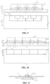
- FIGs. 7-10 are arrangement diagrams of the several magnetoresistive sensor chips 2 in the side mode image identification sensor on the PCB 1.
- FIG. 7(a) is a side view
- FIG. 7(b) is a front view
- side faces 2(1) of the magnetoresistive sensor chips 2 are arranged sequentially along a side face 1(1) of the PCB 1, and there are gaps among them or the gaps are 0.
- Such an arrangement method has the following disadvantages: even if in the situation where the gaps are 0, in the presence of packaging materials, scanning detection areas 2(30) and 2(31) formed on the magnetic image detection surface 3 by adjacent magnetoresistive sensor chips 2 along the scanning direction 4 do not intersect with each other, and thus it is impossible to form continuous detection areas in the scanning direction; therefore, there are undetected areas in the detection of the magnetic image.
- FIGs. 8-10 new arrangement methods of the magnetoresistive sensor chips 2 on the PCB 1 are provided with respect to the problem of the existence of undetected areas of the magnetic image in FIG. 7 , that is, the magnetoresistive sensor chips 2 are arranged on the PCB 1 in a manner of enabling scanning detection areas formed on the magnetic image detection surface 3 by adjacent magnetoresistive sensor chips 2 along a scanning direction to be complementary to or intersect with each other; the arrangements are specifically as follows.
- the first arrangement method of the magnetoresistive sensor chips 2 that can be employed is as follows: the adjacent magnetoresistive sensor chips 2 are on-chip staggered and stacked. As shown in FIG. 8 and FIG. 9 , on the basis of sequential arrangement of the side faces 2(1) of a first layer of magnetoresistive sensor chips 2 along the side face 1(1) of the PCB 1, as shown in FIG.
- a second layer of magnetoresistive sensor chips 2 are added, which are located on the first layer of magnetoresistive sensor chips 2, and each magnetoresistive sensor chip 2 is located in an area between two adjacent magnetoresistive sensor chips 2 in the first layer, so as to form a staggered and stacked structure, such that scanning detection areas 2(32) and 2(33) formed by the two adjacent magnetoresistive sensor chips 2 in the scanning direction 4 are areas complementary to or overlapping with each other, thus ensuring that there is no undetected area in the detection of the magnetic image during scanning.
- the second arrangement method of the magnetoresistive sensor chips 2 that can be employed is as follows: the adjacent magnetoresistive sensor chips 2 are obliquely on-chip stacked. In FIG. 10 , one side of each magnetoresistive sensor chip 2 is cocked away from the front surface 1(1) of the PCB 1, while the other side is on the PCB 1, that is, each magnetoresistive sensor chip 2 is disposed obliquely, such that, in the adjacent magnetoresistive sensor chips 2, a non-cocked side of one magnetoresistive sensor chip 2 is obliquely stacked with a cocked side of the other magnetoresistive sensor chip 2 at an edge, thus ensuring that scanning detection areas 2(34) and 2(35) formed by the adjacent magnetoresistive sensor chips 2 in the scanning direction 4 have overlapping areas and guaranteeing that there is no undetected area in the detection of the magnetic image during scanning.
- FIG. 11 shows a structure of a front detection mode image identification sensor, including a PCB 11 and several magnetoresistive sensor chips 21, wherein the several magnetoresistive sensor chips 21 are located on a front surface 11(2) of the PCB 11, and front surfaces 21(2) thereof are parallel to a magnetic image detection surface 3.
- the magnetic sensing direction thereof may be parallel or perpendicular to the magnetic image detection surface 3, and when the magnetic sensing direction is parallel to the magnetic image detection surface 3, the direction may be parallel or perpendicular to a scanning direction 4.
- a magnetic field generated by the hard magnet will act on the magnetoresistive sensor chips 21 and convert their magnetic field distribution features along the scanning direction 4 to electric signals, thus achieving reading of the magnetic image.
- FIGs. 12-14 show application of the front detection mode image identification sensor in detection of a magnetic image made of a soft magnetic material.
- the front detection mode image identification sensor shown in FIGs. 12-14 further includes a permanent magnet assembly 51 and a housing 6.
- the PCB 11 and the several magnetoresistive sensor chips 21 are located in the housing 6, and the permanent magnet assembly 51 may be located in the housing 6 and may also be partially or wholly located outside the housing 6; the latter may be conducive to reduction of the size of the image identification sensor.
- magnetic sensing directions 71 of the magnetoresistive sensor chips 21 are identical with the scanning direction 4 and parallel to the magnetic image detection surface 3.
- the permanent magnet assembly 51 in the front detection mode image identification sensor shown in FIG. 12 is a concave permanent magnet, of which the geometrical structure is a rectangular groove provided on an upper surface of a block.
- a surface having a greater area and opposite to the front surface 11(2) is its back surface.
- An upper surface of the concave permanent magnet directly faces the back surface of the PCB 11 and is directly in contact with the back surface of the PCB 11, the magnetization direction of the concave permanent magnet is perpendicular to the front surface 11(2) of the PCB 11, and the penetration direction of the rectangular groove, that is, the grooving direction, is perpendicular to the scanning direction 4 and parallel to the magnetic image detection surface 3.
- the permanent magnet assembly 51 in the front detection mode image identification sensor shown in FIG. 13 includes two permanent magnets 51(1) and 51(2) which are symmetrically located on two sides of the magnetoresistive sensor chips 21 along the scanning direction 4 respectively, wherein magnetization directions thereof are perpendicular to the magnetic image detection surface 3 and the front surface 11(2) of the PCB 11, and the magnetization directions are the same.
- the permanent magnet assembly 51 in the front detection mode image identification sensor shown in FIG. 14 includes three permanent magnets 51(3), 51(4) and 51(5), wherein two permanent magnets 51(3) and 51(4) are symmetrically distributed on two sides of the magnetoresistive sensor chips 21 along the scanning direction 4, which are referred to as side permanent magnets, and their magnetization directions are the same and are perpendicular to the magnetic image detection surface 3; another permanent magnet 51(5) is located directly below the PCB 11, that is, the back surface, which is referred to as a back permanent magnet, and its magnetization direction is anti-parallel to the permanent magnets 51(3) and 51(4).
- FIGs. 15-17 are arrangement diagrams of several magnetoresistive sensor chips 21 of the front detection mode image identification sensor on the PCB 11.
- FIGs. 15(a) and 15(b) are a side view and a front view respectively, in which the magnetoresistive sensor chips 21 are arranged into one row on the PCB 11, and the direction of the row is perpendicular to the scanning direction 4 or the magnetic sensing directions 71.
- the magnetoresistive sensor chips 21 are arranged into one row on the PCB 11, and the direction of the row is perpendicular to the scanning direction 4 or the magnetic sensing directions 71.
- scanning detection areas 21(30) and 21(31) formed on the magnetic image detection surface 3 by the adjacent magnetoresistive sensor chips 21 along the scanning direction 4 do not intersect with each other, and thus there are undetected areas on the magnetic image detection surface 3.
- FIG. 16 and FIG. 17 improve the arrangement method of the magnetoresistive sensor chips 21 on the PCB 11.
- FIGs. 16(a) and 16(b) are a side view and a front view of one arrangement method respectively, the scanning direction 4 and the magnetic sensing directions 71 of the magnetoresistive sensor chips 21 are the same, the magnetoresistive sensor chips 21 are disposed obliquely on the front surface 11(2) of the PCB 11, the adjacent magnetoresistive sensor chips 21 are arranged in a staggered manner, and edges of the magnetoresistive sensor chips 21 are mutually staggered, such that scanning detection areas 21(32) and 21(33) formed on the magnetic image detection surface 3 by the adjacent magnetoresistive sensor chips 21 along the scanning direction 4 can overlap with each other, which solves the problem of missed detection.
- FIGs. 17(a) and 17(b) are a side view and a front view of another arrangement method respectively, a third magnetoresistive sensor chip 21 is inserted in a middle position of the row direction of two adjacent magnetoresistive sensor chips 21 and overlaps with the two adjacent magnetoresistive sensor chips 21 at edges, such that scanning detection areas 21(34) and 21(35) of the adjacent magnetoresistive sensor chips 21 overlap with each other, thereby solving the problem of missed detection.
- FIGs. 18-20 are a front view, a side view and a back view of wafer slices of the magnetoresistive sensor chips in the above examples.
- the magnetoresistive sensor chips each include a magnetic sensing unit 42, the magnetoresistive sensing unit 42 is in the front surface of a Si slice 41, and a signal and power pin 43 may be located in the front surface of the Si slice 41 and is led out through wirebonding; a pin 45 may also be formed on the back surface of the Si slice 41 by passing through the Si slice 41 via a TSV via 44. That is, the magnetoresistive sensor chips are of a packaging structure adopting a front bonding pad or a TSV via a back bonding pad of the magnetoresistive sensor chips for wirebonding.
- connection between upper and lower layers of magnetoresistive sensor chips 2 in FIG. 9 may be implemented by connecting onto the PCB 1 through wirebonding, or by direct connection via a pin between the front surface and the back surface.
- employing a TSV back pin compared with the front wirebonding, can reduce a detection distance between the magnetoresistive sensor 21 and the magnetic image detection surface 3 and increase magnetic field intensity.
- FIG. 21 is a composition structure diagram of the magnetic sensing unit 42 in the magnetoresistive sensor chip 2 or 21, and FIG. 21(a) shows a half-bridge structure including two sensing units R1 and R2. The two sensing units R1 and R2 are arranged into two rows and one column, and the two magnetic sensing units R1 and R2 have the same resistance and directly form a half bridge.
- FIG. 21(b) shows a full-bridge structure including four sensing units R1, R2, R3 and R4 and having two outputs Vout+ and Vout-. The four magnetic sensing units R1, R2, R3 and R4 are arranged into two rows and two columns. Two sensing units included in two half bridges forming a full bridge are located in two rows but in different columns respectively.
- FIG. 21(c) shows a half-bridge structure including four sensing units R1, R2, R3 and R4 arranged into two rows and two columns, two magnetic sensing units in the same row are connected in parallel, and then the two rows are connected in series to form a half-bridge structure; two half bridges R1, R2 and R3, R4 share a power source respectively and are grounded, but have a common output end.
- FIG. 21(c) shows a half-bridge structure including four sensing units R1, R2, R3 and R4 arranged into two rows and two columns, two magnetic sensing units in the same row are connected in parallel, and then the two rows are connected in series to form a half-bridge structure; two half bridges R1, R2 and R3, R4 share a power source respectively and are grounded, but have a common output end.
- FIG. 21(c) shows a half-bridge structure including four sensing units R1, R2, R3 and R4 arranged into two rows and two columns, two magnetic sensing units in the same row are connected in parallel, and then
- 21(d) shows a three-sensing-element half-bridge structure arranged into three rows and one column, including three sensing units R1, R2 and R3, wherein two sensing units R1 and R3 located in two side rows have the same resistance, and the resistance is twice that of the sensing unit R2 in the middle row, the sensing units R1 and R3 are connected in parallel and then connected in series with R2 to form a half bridge, and output signal voltages are output from a common end in the middle of R1, R2 and R3.
- the magnetoresistive sensing units may be one of TMR, Hall, AMR or GMR unit. Magnetic sensing directions of various magnetic sensing units are the same.
- FIG. 22 is an arrangement diagram of sensing units in the magnetoresistive sensor chips 2 of the lateral detection mode image identification sensor.
- FIG. 22(a) shows a half-bridge structure, wherein sensing units R1 and R2 form an arrangement of two rows and one column, R1 is located in one row close to the magnetic image detection surface 3 and parallel to the magnetic image detection surface 3, R2 is located in the other row, their magnetic sensing directions are the same and are both in directions 71, the column direction is perpendicular to the magnetic image detection surface 3, and 4 is a scanning direction.
- FIG. 22(b) shows a full-bridge structure or two half-bridge structures, wherein sensing units R1-R4 are arranged into two rows and two columns, wherein R1 and R3 are located in one row close to the magnetic image detection surface 3, R2 and R4 are located in the other row, R1 and R2 form a half bridge, and R3 and R4 form a half bridge.
- FIG. 22(c) shows a three-resistor half-bridge structure including three sensing units R1, R2 and R3 arranged into a structure of three rows and one column, wherein R1 is located in one row close to the magnetic image detection surface 3, R2 is located between R1 and R3, and magnetic sensing directions of R1, R2 and R3 are directions 71 and perpendicular to the magnetic image detection surface 3, and 4 is a scanning direction.
- the sensing units R1, R2, R1-R4 or R1-R3 are located on one side close to the magnetic image detection surface 3.
- FIG. 23 is an arrangement diagram of sensing units in the magnetoresistive sensor chips 21 of the front detection mode image identification sensor, wherein FIGs. 23(a1), 23(a2) and 23(a3) are side views, FIGs. 23(b1), 23(b2) and 23(b3) are front views of the chips 21, and the scanning direction is 4.
- FIG. 23(b1) shows a half-bridge structure including two sensing units R1 and R2, and their arrangement directions are parallel to the sensing directions 71 and identical to the scanning direction 4.
- FIG. 23(b2) shows a full-bridge structure, R1 and R2 are corresponding to one bridge arm therein, R3 and R4 are corresponding to the other bridge arm, and R1, R2 and R3, R4 are arranged along the sensing directions 71.
- FIG. 23(b1) shows a half-bridge structure including two sensing units R1 and R2, and their arrangement directions are parallel to the sensing directions 71 and identical to the scanning direction 4.
- FIG. 23(b2) shows a full-bridge structure,
- FIG. 23(b3) shows a three-element half-bridge structure, the sensing units R1, R2 and R3 are arranged into rows along the scanning direction 4, R2 is located between R1 and R3, and magnetic sensing directions of R1-R3 are 71.
- the contour of the chips 21 in FIG. 23 is a parallel arrangement structure relative to the sensing units, and when the chips are obliquely superposed and arranged, the shape of the chips may rotate by a certain angle relative to arrangement of the sensing units.
- magnetoresistive sensor chips of the full-bridge structure or half-bridge structure may be a single magnetoresistive sensor chip integrated with several sensing units, and may also be replaced with discrete elements of several magnetoresistive sensor chips.
- discrete magnetoresistive sensor chips are integrated with one or more sensing units, and the discrete magnetoresistive sensor chips form a half-bridge or full-bridge structure through interconnection.
- magnetic sensing directions of the sensing units of the magnetoresistive sensor 21 may be parallel or perpendicular to the magnetic image detection surface 3, and when the magnetic sensing directions are parallel to the magnetic image detection surface 3, the direction thereof may be parallel to or perpendicular to the scanning direction 4.
Landscapes
- Physics & Mathematics (AREA)
- General Physics & Mathematics (AREA)
- Condensed Matter Physics & Semiconductors (AREA)
- Measuring Magnetic Variables (AREA)
- Inspection Of Paper Currency And Valuable Securities (AREA)
Claims (9)
- Capteur d'imagerie magnétique magnétorésistif permettant d'identifier une image magnétique dans un plan de détection d'image magnétique (3),dans lequel le capteur d'imagerie estun capteur d'identification d'image en mode de détection latérale ;le capteur d'identification d'image en mode de détection latérale comprend de multiples puces de capteur magnétorésistif (2, 21) sur un PCB (1), le PCB (1) comportant une surface avant (1(2)) qui est perpendiculaire au plan de détection d'image magnétique (3), etcaractérisé par le fait que les multiples puces de capteur magnétorésistif (2, 21) sont situées sur la surface avant du PCB(1), et soit :(i) un côté de chacune des multiples puces de capteur magnétorésistif (2) sur le PCB (1) correspondant au capteur d'identification d'image en mode de détection latérale est incliné à l'opposé de la surface avant du PCB, et l'autre côté est empilé obliquement avec un côté de chacune des puces de capteur magnétorésistif adjacentes (2) ; soit(ii) les puces de capteur magnétorésistif adjacentes (2) dans les multiples puces de capteur magnétorésistif sur le PCB (1) correspondant au capteur d'identification d'image en mode de détection latérale sont décalées et empilées sur puce ;chacune des multiples puces de capteur magnétorésistif (2) comportant une surface avant (2(2)) et une face latérale (2(1)), chaque face latérale (2(1)) des multiples puces de capteur magnétorésistif (2) du capteur d'identification d'image en mode de détection latérale étant parallèle au plan de détection d'image magnétique (3) ; etdans lequel les puces de capteur magnétorésistif adjacentes de chaque capteur d'identification sont complémentaires ou se croisent dans des zones de détection de balayage le long d'une direction de balayage (4) sur le plan de détection d'image magnétique ;comprenant un ensemble d'aimants permanents (5),dans lequel les directions de détection magnétique (7) des multiples puces de capteur magnétorésistif du capteur d'identification d'image en mode de détection latérale sont perpendiculaires au plan de détection d'image magnétique (3) ; etdans lequel pour le capteur d'identification d'image en mode de détection latérale, l'ensemble d'aimants permanents (5) comprend une structure comportant une ouverture vers le plan de détection d'image magnétique et formée par un aimant permanent (5(7)) et un aimant doux en forme de L (5(8)), qui sont situés du même côté du PCB (1), et l'aimant doux en forme de L est situé entre l'aimant permanent et le PCB, l'aimant permanent est situé sur le bas de l'aimant doux en forme de L et la direction de magnétisation de celui-ci est perpendiculaire au plan de détection d'image magnétique (3), et une face latérale de l'aimant doux en forme de L est parallèle au PCB.
- Capteur d'imagerie magnétique magnétorésistif permettant d'identifier une image magnétique selon la revendication 1, dans lequel les puces de capteur magnétorésistif sont une structure en demi-pont comprenant deux, trois ou quatre unités de détection magnétique (R1, R2, R3, R4) disposées en deux rangées et une colonne, trois rangées et une colonne, ou deux rangées et deux colonnes respectivement, et les directions de détection magnétique des différentes unités de détection magnétique sont identiques ;lorsque les puces de capteur magnétique magnétorésistif comprennent deux unités de détection magnétique, les deux unités de détection magnétique comportent la même résistance et forment directement un demi-pont ;lorsque les puces de capteurs magnétiques magnétorésistifs comprennent trois unités de détection magnétiques, la résistance de l'unité de détection de la rangée du milieu est la moitié des résistances des deux unités de détection des deux rangées latérales, et les deux unités de détection sur les deux rangées latérales, après avoir été connectées en parallèle, forment une structure en demi-pont avec l'unité de détection de la rangée du milieu ;lorsque les puces de capteur magnétique magnétorésistif comprennent quatre unités de détection magnétique, les résistances des quatre unités de détection sont les mêmes, et deux unités de détection magnétiques dans la même rangée sont connectées en parallèle et ensuite les deux rangées sont connectées en série pour former une structure en demi-pont ;dans le capteur d'identification d'image en mode de détection latérale, la direction de colonne de celui-ci est perpendiculaire au plan de détection d'image magnétique (3), et pendant la mise en boîtier, les unités de détection magnétique sont situées sur un côté des puces à proximité du plan de détection d'image magnétique.
- Capteur d'imagerie magnétique magnétorésistif permettant d'identifier une image magnétique selon la revendication 2, dans lequel les puces de capteur magnétorésistif (2, 21) de la structure en demi-pont sont une puce de capteur magnétorésistif unique intégrée à plusieurs unités de détection, ou une combinaison interconnectée d'éléments discrets de multiples puces de capteur magnétorésistif intégrées à une ou plusieurs unités de détection.
- Capteur d'imagerie magnétique magnétorésistif permettant d'identifier une image magnétique selon l'une quelconque des revendications 1 à 3, dans lequel les puces de capteur magnétorésistif sont une structure en pont complet comprenant quatre unités de détection magnétique (R1, R2, R3, R4), et les directions de détection magnétique des diverses unités de détection magnétique sont identiques, les quatre unités de détection magnétiques sont disposées en deux rangées et deux colonnes, deux unités de détection comprises dans deux demi-ponts formant un pont complet sont situées sur deux rangées mais dans des colonnes différentes respectivement ;
dans le capteur d'identification d'image en mode de détection latérale, la direction de colonne de celui-ci est perpendiculaire au plan de détection d'image magnétique (3), et pendant la mise en boîtier, les unités de détection sont situées sur un côté des puces à proximité du plan de détection d'image magnétique. - Capteur d'imagerie magnétique magnétorésistif permettant d'identifier une image magnétique selon la revendication 4, dans lequel les puces de capteur magnétorésistif (2, 21) de la structure en pont complet sont une puce de capteur magnétorésistif unique intégrée à plusieurs unités de détection, ou une combinaison interconnectée d'éléments discrets de multiples puces de capteur magnétorésistif intégrées à une ou plusieurs unités de détection.
- Capteur d'imagerie magnétique magnétorésistif permettant d'identifier une image magnétique selon la revendication 1, comprenant en outre un boîtier (6) dans lequel le PCB (1) et les multiples puces de capteur magnétorésistif (2, 21) sont placés ;
l'ensemble d'aimants permanents étant partiellement ou entièrement placé dans le boîtier, ou entièrement situé à l'extérieur du boîtier. - Capteur d'imagerie magnétique magnétorésistif permettant d'identifier une image magnétique selon la revendication 1, dans lequel les puces de capteur magnétorésistif sont d'une structure de boîtier adoptant un plot de liaison avant ou un TSV via un plot de liaison arrière (45) des puces de capteur magnétorésistif pour la liaison par fils.
- Capteur d'imagerie magnétique magnétorésistif permettant d'identifier une image magnétique selon la revendication 1, dans lequel les unités de détection magnétique dans les puces de capteur magnétique magnétorésistif sont d'un type parmi les type AMR, Hall, GMR ou TMR de capteur magnétorésistif.
- Capteur d'imagerie magnétique magnétorésistif permettant d'identifier une image magnétique selon la revendication 1, dans lequel chaque face latérale des puces de capteur magnétorésistif correspondant au capteur d'identification d'image en mode de détection latérale est coplanaire avec une face latérale du PCB ou parallèle au plan de détection d'image magnétique.
Applications Claiming Priority (2)
| Application Number | Priority Date | Filing Date | Title |
|---|---|---|---|
| CN201410113778.3A CN103927811B (zh) | 2014-03-25 | 2014-03-25 | 一种磁电阻磁性图像识别传感器 |
| PCT/CN2015/074982 WO2015144046A1 (fr) | 2014-03-25 | 2015-03-24 | Capteur à magnétorésistance permettant d'identifier une image magnétique |
Publications (3)
| Publication Number | Publication Date |
|---|---|
| EP3125202A1 EP3125202A1 (fr) | 2017-02-01 |
| EP3125202A4 EP3125202A4 (fr) | 2017-12-20 |
| EP3125202B1 true EP3125202B1 (fr) | 2025-01-22 |
Family
ID=51146021
Family Applications (1)
| Application Number | Title | Priority Date | Filing Date |
|---|---|---|---|
| EP15770409.9A Active EP3125202B1 (fr) | 2014-03-25 | 2015-03-24 | Capteur à magnétorésistance permettant d'identifier d'images magnétiques |
Country Status (5)
| Country | Link |
|---|---|
| US (1) | US10598743B2 (fr) |
| EP (1) | EP3125202B1 (fr) |
| JP (1) | JP6535024B2 (fr) |
| CN (1) | CN103927811B (fr) |
| WO (1) | WO2015144046A1 (fr) |
Families Citing this family (9)
| Publication number | Priority date | Publication date | Assignee | Title |
|---|---|---|---|---|
| CN103927811B (zh) * | 2014-03-25 | 2016-09-14 | 江苏多维科技有限公司 | 一种磁电阻磁性图像识别传感器 |
| CN104201168B (zh) * | 2014-09-16 | 2017-01-25 | 山东华芯半导体有限公司 | 一种芯片倾斜堆叠的圆片级封装单元及封装方法 |
| JP6326442B2 (ja) * | 2016-03-30 | 2018-05-16 | Kyb株式会社 | 磁気検出ユニット及びこれを備えるストローク検出装置 |
| JP7172178B2 (ja) * | 2018-06-27 | 2022-11-16 | Tdk株式会社 | 磁気センサ |
| JP7070532B2 (ja) * | 2019-11-19 | 2022-05-18 | Tdk株式会社 | 磁気センサ |
| DE102021114943A1 (de) * | 2021-06-10 | 2022-12-15 | Infineon Technologies Ag | Sensorvorrichtungen mit Weichmagneten und zugehörige Herstellungsverfahren |
| GB2615816B (en) * | 2022-02-21 | 2026-04-22 | The Governor & Company Of The Bank Of England | Document recognition device |
| CN115079061B (zh) * | 2022-05-05 | 2025-04-29 | 歌尔微电子股份有限公司 | 微机电系统差分磁传感器、传感器单体及电子设备 |
| WO2025258350A1 (fr) * | 2024-06-12 | 2025-12-18 | グローリー株式会社 | Capteur de ligne magnétique, dispositif d'identification de feuille de papier et dispositif de traitement de feuille de papier |
Citations (4)
| Publication number | Priority date | Publication date | Assignee | Title |
|---|---|---|---|---|
| US20030067299A1 (en) * | 2001-09-28 | 2003-04-10 | Koji Shinmura | Magnetic sensor |
| CN102968845A (zh) * | 2012-10-31 | 2013-03-13 | 江苏多维科技有限公司 | 一种被磁偏置的敏感方向平行于检测面的验钞磁头 |
| US20130127457A1 (en) * | 2010-07-30 | 2013-05-23 | Mitsubishi Electric Corporation | Magnetic substance detection device |
| CN103226865A (zh) * | 2013-04-16 | 2013-07-31 | 白建民 | 一种基于磁电阻技术检测磁性图形表面磁场的磁头 |
Family Cites Families (17)
| Publication number | Priority date | Publication date | Assignee | Title |
|---|---|---|---|---|
| JPH0722668A (ja) * | 1993-06-23 | 1995-01-24 | Nec Corp | 磁気抵抗効果素子 |
| JP2005249468A (ja) * | 2004-03-02 | 2005-09-15 | Murata Mfg Co Ltd | 長尺型磁気センサ |
| JP2008515043A (ja) * | 2004-09-27 | 2008-05-08 | コーニンクレッカ フィリップス エレクトロニクス エヌ ヴィ | 入力装置用の磁気センサ |
| JP2006171953A (ja) * | 2004-12-14 | 2006-06-29 | Laurel Seiki Kk | 紙葉類検出装置 |
| JP2006350820A (ja) * | 2005-06-17 | 2006-12-28 | Toshiba Corp | 紙葉類識別装置 |
| CN104123781B (zh) * | 2010-02-05 | 2017-01-18 | 日本电产三协株式会社 | 磁性图案检测装置 |
| JP5719515B2 (ja) * | 2010-02-05 | 2015-05-20 | 日本電産サンキョー株式会社 | 磁気センサ装置 |
| CN201725379U (zh) * | 2010-06-24 | 2011-01-26 | 深圳市怡化电脑有限公司 | Atm机巨磁电阻验钞磁头 |
| JP5195963B2 (ja) * | 2010-11-16 | 2013-05-15 | 三菱電機株式会社 | 磁気センサ装置 |
| WO2012015012A1 (fr) * | 2010-07-30 | 2012-02-02 | 三菱電機株式会社 | Dispositif capteur magnétique |
| US9250476B2 (en) * | 2012-03-30 | 2016-02-02 | Dic Corporation | Liquid crystal display device and method for producing the same |
| CN103632431B (zh) * | 2012-08-21 | 2018-03-09 | 北京嘉岳同乐极电子有限公司 | 磁图像传感器及鉴伪方法 |
| CN203038357U (zh) * | 2012-10-31 | 2013-07-03 | 江苏多维科技有限公司 | 一种被磁偏置的敏感方向平行于检测面的验钞磁头 |
| CN202916902U (zh) * | 2012-10-31 | 2013-05-01 | 江苏多维科技有限公司 | 一种被磁偏置的敏感方向平行于检测面的验钞磁头 |
| CN203217645U (zh) * | 2013-04-16 | 2013-09-25 | 无锡乐尔科技有限公司 | 识别磁条上磁性图形的磁矩取向装置 |
| CN103927811B (zh) | 2014-03-25 | 2016-09-14 | 江苏多维科技有限公司 | 一种磁电阻磁性图像识别传感器 |
| CN203812310U (zh) * | 2014-03-25 | 2014-09-03 | 江苏多维科技有限公司 | 一种磁电阻磁性图像识别传感器 |
-
2014
- 2014-03-25 CN CN201410113778.3A patent/CN103927811B/zh active Active
-
2015
- 2015-03-24 WO PCT/CN2015/074982 patent/WO2015144046A1/fr not_active Ceased
- 2015-03-24 US US15/128,821 patent/US10598743B2/en active Active
- 2015-03-24 JP JP2016559210A patent/JP6535024B2/ja active Active
- 2015-03-24 EP EP15770409.9A patent/EP3125202B1/fr active Active
Patent Citations (4)
| Publication number | Priority date | Publication date | Assignee | Title |
|---|---|---|---|---|
| US20030067299A1 (en) * | 2001-09-28 | 2003-04-10 | Koji Shinmura | Magnetic sensor |
| US20130127457A1 (en) * | 2010-07-30 | 2013-05-23 | Mitsubishi Electric Corporation | Magnetic substance detection device |
| CN102968845A (zh) * | 2012-10-31 | 2013-03-13 | 江苏多维科技有限公司 | 一种被磁偏置的敏感方向平行于检测面的验钞磁头 |
| CN103226865A (zh) * | 2013-04-16 | 2013-07-31 | 白建民 | 一种基于磁电阻技术检测磁性图形表面磁场的磁头 |
Also Published As
| Publication number | Publication date |
|---|---|
| WO2015144046A1 (fr) | 2015-10-01 |
| EP3125202A4 (fr) | 2017-12-20 |
| US10598743B2 (en) | 2020-03-24 |
| US20170371005A1 (en) | 2017-12-28 |
| CN103927811B (zh) | 2016-09-14 |
| JP2017514114A (ja) | 2017-06-01 |
| CN103927811A (zh) | 2014-07-16 |
| EP3125202A1 (fr) | 2017-02-01 |
| JP6535024B2 (ja) | 2019-06-26 |
Similar Documents
| Publication | Publication Date | Title |
|---|---|---|
| US10598743B2 (en) | Magnetoresistive magnetic imaging sensor | |
| US10109131B2 (en) | Sensor device including magnetoresistive sensor element and pre-magnetization device | |
| JP6209674B2 (ja) | 磁気抵抗技術に基づいて磁気パターンの表面磁界を検出する磁気ヘッド | |
| US20090152356A1 (en) | Non-contact magnetic pattern recognition sensor | |
| JP6359858B2 (ja) | 磁界検出装置および磁気識別装置 | |
| KR20010075724A (ko) | 차분 vgmr 센서 | |
| CN113302693A (zh) | 磁识别传感器 | |
| US10008064B2 (en) | Measuring device for measuring magnetic properties of the surroundings of the measuring device | |
| US10222431B2 (en) | Measuring device with pre-magnetizing magnet | |
| US10168396B2 (en) | Low fly height in-plane magnetic image sensor chip | |
| WO2016170886A1 (fr) | Dispositif de capteur magnétique | |
| Smith et al. | Chip-size magnetic sensor arrays | |
| CN103544764B (zh) | 一种用于识别磁性介质的传感器 | |
| CN203812310U (zh) | 一种磁电阻磁性图像识别传感器 | |
| CN203490758U (zh) | 一种用于识别磁性介质的传感器 | |
| CN203858698U (zh) | 一种低飞移高度面内磁性图像识别传感器芯片 | |
| CN104392537A (zh) | 软硬磁磁头 | |
| JP4338090B2 (ja) | 磁性粉付着媒体又は磁性膜付着媒体検出装置 | |
| CN204883909U (zh) | 一种硬币检测探头及其检测系统 | |
| JP2019179435A (ja) | 磁気識別センサおよび磁気識別装置 | |
| CN105093135A (zh) | 磁头以及磁性介质的评价方法 | |
| CN103456072B (zh) | 一种用于识别磁性介质的传感器 | |
| CN204215468U (zh) | 软硬磁磁头 |
Legal Events
| Date | Code | Title | Description |
|---|---|---|---|
| STAA | Information on the status of an ep patent application or granted ep patent |
Free format text: STATUS: THE INTERNATIONAL PUBLICATION HAS BEEN MADE |
|
| PUAI | Public reference made under article 153(3) epc to a published international application that has entered the european phase |
Free format text: ORIGINAL CODE: 0009012 |
|
| STAA | Information on the status of an ep patent application or granted ep patent |
Free format text: STATUS: REQUEST FOR EXAMINATION WAS MADE |
|
| 17P | Request for examination filed |
Effective date: 20161020 |
|
| AK | Designated contracting states |
Kind code of ref document: A1 Designated state(s): AL AT BE BG CH CY CZ DE DK EE ES FI FR GB GR HR HU IE IS IT LI LT LU LV MC MK MT NL NO PL PT RO RS SE SI SK SM TR |
|
| AX | Request for extension of the european patent |
Extension state: BA ME |
|
| DAV | Request for validation of the european patent (deleted) | ||
| DAX | Request for extension of the european patent (deleted) | ||
| A4 | Supplementary search report drawn up and despatched |
Effective date: 20171116 |
|
| RIC1 | Information provided on ipc code assigned before grant |
Ipc: G07D 7/04 20160101AFI20171110BHEP |
|
| STAA | Information on the status of an ep patent application or granted ep patent |
Free format text: STATUS: EXAMINATION IS IN PROGRESS |
|
| 17Q | First examination report despatched |
Effective date: 20210413 |
|
| RAP3 | Party data changed (applicant data changed or rights of an application transferred) |
Owner name: MULTIDIMENSION TECHNOLOGY CO., LTD. |
|
| RIN1 | Information on inventor provided before grant (corrected) |
Inventor name: ZHOU, ZHIMIN Inventor name: DEAK, JAMES GEZA Inventor name: ZHANG, XIAOJUN Inventor name: LEI, XIAOFENG Inventor name: XUE, SONGSHENG |
|
| RAP3 | Party data changed (applicant data changed or rights of an application transferred) |
Owner name: MULTIDIMENSION TECHNOLOGY CO., LTD. |
|
| RAP3 | Party data changed (applicant data changed or rights of an application transferred) |
Owner name: MULTIDIMENSION TECHNOLOGY CO., LTD. |
|
| RIN1 | Information on inventor provided before grant (corrected) |
Inventor name: ZHOU, ZHIMIN Inventor name: DEAK, JAMES GEZA Inventor name: ZHANG, XIAOJUN Inventor name: LEI, XIAOFENG Inventor name: XUE, SONGSHENG |
|
| RAP3 | Party data changed (applicant data changed or rights of an application transferred) |
Owner name: MULTIDIMENSION TECHNOLOGY CO., LTD. |
|
| RIN1 | Information on inventor provided before grant (corrected) |
Inventor name: ZHOU, ZHIMIN Inventor name: DEAK, JAMES GEZA Inventor name: ZHANG, XIAOJUN Inventor name: LEI, XIAOFENG Inventor name: XUE, SONGSHENG |
|
| P01 | Opt-out of the competence of the unified patent court (upc) registered |
Effective date: 20230626 |
|
| GRAP | Despatch of communication of intention to grant a patent |
Free format text: ORIGINAL CODE: EPIDOSNIGR1 |
|
| STAA | Information on the status of an ep patent application or granted ep patent |
Free format text: STATUS: GRANT OF PATENT IS INTENDED |
|
| INTG | Intention to grant announced |
Effective date: 20240514 |
|
| GRAJ | Information related to disapproval of communication of intention to grant by the applicant or resumption of examination proceedings by the epo deleted |
Free format text: ORIGINAL CODE: EPIDOSDIGR1 |
|
| STAA | Information on the status of an ep patent application or granted ep patent |
Free format text: STATUS: EXAMINATION IS IN PROGRESS |
|
| REG | Reference to a national code |
Ref country code: DE Ref legal event code: R079 Free format text: PREVIOUS MAIN CLASS: G07D0007040000 Ipc: G01R0033090000 Ref country code: DE Ref legal event code: R079 Ref document number: 602015090899 Country of ref document: DE Free format text: PREVIOUS MAIN CLASS: G07D0007040000 Ipc: G01R0033090000 |
|
| GRAP | Despatch of communication of intention to grant a patent |
Free format text: ORIGINAL CODE: EPIDOSNIGR1 |
|
| STAA | Information on the status of an ep patent application or granted ep patent |
Free format text: STATUS: GRANT OF PATENT IS INTENDED |
|
| INTG | Intention to grant announced |
Effective date: 20240924 |
|
| RIC1 | Information provided on ipc code assigned before grant |
Ipc: G07D 7/20 20160101ALI20240916BHEP Ipc: G07D 7/04 20160101ALI20240916BHEP Ipc: G01R 33/09 20060101AFI20240916BHEP |
|
| GRAS | Grant fee paid |
Free format text: ORIGINAL CODE: EPIDOSNIGR3 |
|
| GRAA | (expected) grant |
Free format text: ORIGINAL CODE: 0009210 |
|
| STAA | Information on the status of an ep patent application or granted ep patent |
Free format text: STATUS: THE PATENT HAS BEEN GRANTED |
|
| AK | Designated contracting states |
Kind code of ref document: B1 Designated state(s): AL AT BE BG CH CY CZ DE DK EE ES FI FR GB GR HR HU IE IS IT LI LT LU LV MC MK MT NL NO PL PT RO RS SE SI SK SM TR |
|
| REG | Reference to a national code |
Ref country code: GB Ref legal event code: FG4D |
|
| REG | Reference to a national code |
Ref country code: CH Ref legal event code: EP |
|
| REG | Reference to a national code |
Ref country code: IE Ref legal event code: FG4D |
|
| REG | Reference to a national code |
Ref country code: DE Ref legal event code: R096 Ref document number: 602015090899 Country of ref document: DE |
|
| REG | Reference to a national code |
Ref country code: NL Ref legal event code: MP Effective date: 20250122 |
|
| PG25 | Lapsed in a contracting state [announced via postgrant information from national office to epo] |
Ref country code: NL Free format text: LAPSE BECAUSE OF FAILURE TO SUBMIT A TRANSLATION OF THE DESCRIPTION OR TO PAY THE FEE WITHIN THE PRESCRIBED TIME-LIMIT Effective date: 20250122 |
|
| PG25 | Lapsed in a contracting state [announced via postgrant information from national office to epo] |
Ref country code: RS Free format text: LAPSE BECAUSE OF FAILURE TO SUBMIT A TRANSLATION OF THE DESCRIPTION OR TO PAY THE FEE WITHIN THE PRESCRIBED TIME-LIMIT Effective date: 20250422 |
|
| PG25 | Lapsed in a contracting state [announced via postgrant information from national office to epo] |
Ref country code: FI Free format text: LAPSE BECAUSE OF FAILURE TO SUBMIT A TRANSLATION OF THE DESCRIPTION OR TO PAY THE FEE WITHIN THE PRESCRIBED TIME-LIMIT Effective date: 20250122 |
|
| PG25 | Lapsed in a contracting state [announced via postgrant information from national office to epo] |
Ref country code: PL Free format text: LAPSE BECAUSE OF FAILURE TO SUBMIT A TRANSLATION OF THE DESCRIPTION OR TO PAY THE FEE WITHIN THE PRESCRIBED TIME-LIMIT Effective date: 20250122 |
|
| PG25 | Lapsed in a contracting state [announced via postgrant information from national office to epo] |
Ref country code: ES Free format text: LAPSE BECAUSE OF FAILURE TO SUBMIT A TRANSLATION OF THE DESCRIPTION OR TO PAY THE FEE WITHIN THE PRESCRIBED TIME-LIMIT Effective date: 20250122 |
|
| REG | Reference to a national code |
Ref country code: LT Ref legal event code: MG9D |
|
| PG25 | Lapsed in a contracting state [announced via postgrant information from national office to epo] |
Ref country code: IS Free format text: LAPSE BECAUSE OF FAILURE TO SUBMIT A TRANSLATION OF THE DESCRIPTION OR TO PAY THE FEE WITHIN THE PRESCRIBED TIME-LIMIT Effective date: 20250522 Ref country code: NO Free format text: LAPSE BECAUSE OF FAILURE TO SUBMIT A TRANSLATION OF THE DESCRIPTION OR TO PAY THE FEE WITHIN THE PRESCRIBED TIME-LIMIT Effective date: 20250422 |
|
| REG | Reference to a national code |
Ref country code: AT Ref legal event code: MK05 Ref document number: 1761847 Country of ref document: AT Kind code of ref document: T Effective date: 20250122 |
|
| PG25 | Lapsed in a contracting state [announced via postgrant information from national office to epo] |
Ref country code: HR Free format text: LAPSE BECAUSE OF FAILURE TO SUBMIT A TRANSLATION OF THE DESCRIPTION OR TO PAY THE FEE WITHIN THE PRESCRIBED TIME-LIMIT Effective date: 20250122 |
|
| PG25 | Lapsed in a contracting state [announced via postgrant information from national office to epo] |
Ref country code: PT Free format text: LAPSE BECAUSE OF FAILURE TO SUBMIT A TRANSLATION OF THE DESCRIPTION OR TO PAY THE FEE WITHIN THE PRESCRIBED TIME-LIMIT Effective date: 20250522 Ref country code: LV Free format text: LAPSE BECAUSE OF FAILURE TO SUBMIT A TRANSLATION OF THE DESCRIPTION OR TO PAY THE FEE WITHIN THE PRESCRIBED TIME-LIMIT Effective date: 20250122 |
|
| PG25 | Lapsed in a contracting state [announced via postgrant information from national office to epo] |
Ref country code: GR Free format text: LAPSE BECAUSE OF FAILURE TO SUBMIT A TRANSLATION OF THE DESCRIPTION OR TO PAY THE FEE WITHIN THE PRESCRIBED TIME-LIMIT Effective date: 20250423 Ref country code: BG Free format text: LAPSE BECAUSE OF FAILURE TO SUBMIT A TRANSLATION OF THE DESCRIPTION OR TO PAY THE FEE WITHIN THE PRESCRIBED TIME-LIMIT Effective date: 20250122 |
|
| PG25 | Lapsed in a contracting state [announced via postgrant information from national office to epo] |
Ref country code: AT Free format text: LAPSE BECAUSE OF FAILURE TO SUBMIT A TRANSLATION OF THE DESCRIPTION OR TO PAY THE FEE WITHIN THE PRESCRIBED TIME-LIMIT Effective date: 20250122 |
|
| PG25 | Lapsed in a contracting state [announced via postgrant information from national office to epo] |
Ref country code: SE Free format text: LAPSE BECAUSE OF FAILURE TO SUBMIT A TRANSLATION OF THE DESCRIPTION OR TO PAY THE FEE WITHIN THE PRESCRIBED TIME-LIMIT Effective date: 20250122 |
|
| PG25 | Lapsed in a contracting state [announced via postgrant information from national office to epo] |
Ref country code: SM Free format text: LAPSE BECAUSE OF FAILURE TO SUBMIT A TRANSLATION OF THE DESCRIPTION OR TO PAY THE FEE WITHIN THE PRESCRIBED TIME-LIMIT Effective date: 20250122 |
|
| PG25 | Lapsed in a contracting state [announced via postgrant information from national office to epo] |
Ref country code: DK Free format text: LAPSE BECAUSE OF FAILURE TO SUBMIT A TRANSLATION OF THE DESCRIPTION OR TO PAY THE FEE WITHIN THE PRESCRIBED TIME-LIMIT Effective date: 20250122 |
|
| PG25 | Lapsed in a contracting state [announced via postgrant information from national office to epo] |
Ref country code: MC Free format text: LAPSE BECAUSE OF FAILURE TO SUBMIT A TRANSLATION OF THE DESCRIPTION OR TO PAY THE FEE WITHIN THE PRESCRIBED TIME-LIMIT Effective date: 20250122 |
|
| PG25 | Lapsed in a contracting state [announced via postgrant information from national office to epo] |
Ref country code: IT Free format text: LAPSE BECAUSE OF FAILURE TO SUBMIT A TRANSLATION OF THE DESCRIPTION OR TO PAY THE FEE WITHIN THE PRESCRIBED TIME-LIMIT Effective date: 20250122 |
|
| PG25 | Lapsed in a contracting state [announced via postgrant information from national office to epo] |
Ref country code: EE Free format text: LAPSE BECAUSE OF FAILURE TO SUBMIT A TRANSLATION OF THE DESCRIPTION OR TO PAY THE FEE WITHIN THE PRESCRIBED TIME-LIMIT Effective date: 20250122 Ref country code: CZ Free format text: LAPSE BECAUSE OF FAILURE TO SUBMIT A TRANSLATION OF THE DESCRIPTION OR TO PAY THE FEE WITHIN THE PRESCRIBED TIME-LIMIT Effective date: 20250122 |
|
| REG | Reference to a national code |
Ref country code: CH Ref legal event code: H13 Free format text: ST27 STATUS EVENT CODE: U-0-0-H10-H13 (AS PROVIDED BY THE NATIONAL OFFICE) Effective date: 20251023 Ref country code: DE Ref legal event code: R097 Ref document number: 602015090899 Country of ref document: DE |
|
| PG25 | Lapsed in a contracting state [announced via postgrant information from national office to epo] |
Ref country code: RO Free format text: LAPSE BECAUSE OF FAILURE TO SUBMIT A TRANSLATION OF THE DESCRIPTION OR TO PAY THE FEE WITHIN THE PRESCRIBED TIME-LIMIT Effective date: 20250122 |
|
| PG25 | Lapsed in a contracting state [announced via postgrant information from national office to epo] |
Ref country code: SK Free format text: LAPSE BECAUSE OF FAILURE TO SUBMIT A TRANSLATION OF THE DESCRIPTION OR TO PAY THE FEE WITHIN THE PRESCRIBED TIME-LIMIT Effective date: 20250122 |
|
| PG25 | Lapsed in a contracting state [announced via postgrant information from national office to epo] |
Ref country code: LU Free format text: LAPSE BECAUSE OF NON-PAYMENT OF DUE FEES Effective date: 20250324 |
|
| PLBE | No opposition filed within time limit |
Free format text: ORIGINAL CODE: 0009261 |
|
| STAA | Information on the status of an ep patent application or granted ep patent |
Free format text: STATUS: NO OPPOSITION FILED WITHIN TIME LIMIT |
|
| REG | Reference to a national code |
Ref country code: BE Ref legal event code: MM Effective date: 20250331 |
|
| 26N | No opposition filed |
Effective date: 20251023 |
|
| PG25 | Lapsed in a contracting state [announced via postgrant information from national office to epo] |
Ref country code: BE Free format text: LAPSE BECAUSE OF NON-PAYMENT OF DUE FEES Effective date: 20250331 |
|
| PG25 | Lapsed in a contracting state [announced via postgrant information from national office to epo] |
Ref country code: CH Free format text: LAPSE BECAUSE OF NON-PAYMENT OF DUE FEES Effective date: 20250331 |
|
| PG25 | Lapsed in a contracting state [announced via postgrant information from national office to epo] |
Ref country code: IE Free format text: LAPSE BECAUSE OF NON-PAYMENT OF DUE FEES Effective date: 20250324 |
|
| PGFP | Annual fee paid to national office [announced via postgrant information from national office to epo] |
Ref country code: GB Payment date: 20260327 Year of fee payment: 12 |
|
| PGFP | Annual fee paid to national office [announced via postgrant information from national office to epo] |
Ref country code: DE Payment date: 20260327 Year of fee payment: 12 |
|
| PGFP | Annual fee paid to national office [announced via postgrant information from national office to epo] |
Ref country code: FR Payment date: 20260325 Year of fee payment: 12 |