EP3128552A1 - Circuit sur plaquette - Google Patents
Circuit sur plaquette Download PDFInfo
- Publication number
- EP3128552A1 EP3128552A1 EP14887860.6A EP14887860A EP3128552A1 EP 3128552 A1 EP3128552 A1 EP 3128552A1 EP 14887860 A EP14887860 A EP 14887860A EP 3128552 A1 EP3128552 A1 EP 3128552A1
- Authority
- EP
- European Patent Office
- Prior art keywords
- bonding
- electrode
- wires
- bonding wires
- bonding pad
- Prior art date
- Legal status (The legal status is an assumption and is not a legal conclusion. Google has not performed a legal analysis and makes no representation as to the accuracy of the status listed.)
- Withdrawn
Links
Images
Classifications
-
- H—ELECTRICITY
- H10—SEMICONDUCTOR DEVICES; ELECTRIC SOLID-STATE DEVICES NOT OTHERWISE PROVIDED FOR
- H10H—INORGANIC LIGHT-EMITTING SEMICONDUCTOR DEVICES HAVING POTENTIAL BARRIERS
- H10H20/00—Individual inorganic light-emitting semiconductor devices having potential barriers, e.g. light-emitting diodes [LED]
- H10H20/80—Constructional details
- H10H20/85—Packages
- H10H20/857—Interconnections, e.g. lead-frames, bond wires or solder balls
-
- H—ELECTRICITY
- H10—SEMICONDUCTOR DEVICES; ELECTRIC SOLID-STATE DEVICES NOT OTHERWISE PROVIDED FOR
- H10W—GENERIC PACKAGES, INTERCONNECTIONS, CONNECTORS OR OTHER CONSTRUCTIONAL DETAILS OF DEVICES COVERED BY CLASS H10
- H10W72/00—Interconnections or connectors in packages
- H10W72/50—Bond wires
-
- H—ELECTRICITY
- H10—SEMICONDUCTOR DEVICES; ELECTRIC SOLID-STATE DEVICES NOT OTHERWISE PROVIDED FOR
- H10W—GENERIC PACKAGES, INTERCONNECTIONS, CONNECTORS OR OTHER CONSTRUCTIONAL DETAILS OF DEVICES COVERED BY CLASS H10
- H10W70/00—Package substrates; Interposers; Redistribution layers [RDL]
- H10W70/60—Insulating or insulated package substrates; Interposers; Redistribution layers
- H10W70/62—Insulating or insulated package substrates; Interposers; Redistribution layers characterised by their interconnections
- H10W70/65—Shapes or dispositions of interconnections
-
- H—ELECTRICITY
- H10—SEMICONDUCTOR DEVICES; ELECTRIC SOLID-STATE DEVICES NOT OTHERWISE PROVIDED FOR
- H10W—GENERIC PACKAGES, INTERCONNECTIONS, CONNECTORS OR OTHER CONSTRUCTIONAL DETAILS OF DEVICES COVERED BY CLASS H10
- H10W72/00—Interconnections or connectors in packages
- H10W72/071—Connecting or disconnecting
- H10W72/075—Connecting or disconnecting of bond wires
- H10W72/07551—Connecting or disconnecting of bond wires characterised by changes in properties of the bond wires during the connecting
- H10W72/07553—Connecting or disconnecting of bond wires characterised by changes in properties of the bond wires during the connecting changes in shapes
-
- H—ELECTRICITY
- H10—SEMICONDUCTOR DEVICES; ELECTRIC SOLID-STATE DEVICES NOT OTHERWISE PROVIDED FOR
- H10W—GENERIC PACKAGES, INTERCONNECTIONS, CONNECTORS OR OTHER CONSTRUCTIONAL DETAILS OF DEVICES COVERED BY CLASS H10
- H10W72/00—Interconnections or connectors in packages
- H10W72/30—Die-attach connectors
- H10W72/321—Structures or relative sizes of die-attach connectors
- H10W72/325—Die-attach connectors having a filler embedded in a matrix
-
- H—ELECTRICITY
- H10—SEMICONDUCTOR DEVICES; ELECTRIC SOLID-STATE DEVICES NOT OTHERWISE PROVIDED FOR
- H10W—GENERIC PACKAGES, INTERCONNECTIONS, CONNECTORS OR OTHER CONSTRUCTIONAL DETAILS OF DEVICES COVERED BY CLASS H10
- H10W72/00—Interconnections or connectors in packages
- H10W72/30—Die-attach connectors
- H10W72/351—Materials of die-attach connectors
- H10W72/352—Materials of die-attach connectors comprising metals or metalloids, e.g. solders
-
- H—ELECTRICITY
- H10—SEMICONDUCTOR DEVICES; ELECTRIC SOLID-STATE DEVICES NOT OTHERWISE PROVIDED FOR
- H10W—GENERIC PACKAGES, INTERCONNECTIONS, CONNECTORS OR OTHER CONSTRUCTIONAL DETAILS OF DEVICES COVERED BY CLASS H10
- H10W72/00—Interconnections or connectors in packages
- H10W72/50—Bond wires
- H10W72/531—Shapes of wire connectors
-
- H—ELECTRICITY
- H10—SEMICONDUCTOR DEVICES; ELECTRIC SOLID-STATE DEVICES NOT OTHERWISE PROVIDED FOR
- H10W—GENERIC PACKAGES, INTERCONNECTIONS, CONNECTORS OR OTHER CONSTRUCTIONAL DETAILS OF DEVICES COVERED BY CLASS H10
- H10W72/00—Interconnections or connectors in packages
- H10W72/50—Bond wires
- H10W72/531—Shapes of wire connectors
- H10W72/5366—Shapes of wire connectors the bond wires having kinks
-
- H—ELECTRICITY
- H10—SEMICONDUCTOR DEVICES; ELECTRIC SOLID-STATE DEVICES NOT OTHERWISE PROVIDED FOR
- H10W—GENERIC PACKAGES, INTERCONNECTIONS, CONNECTORS OR OTHER CONSTRUCTIONAL DETAILS OF DEVICES COVERED BY CLASS H10
- H10W72/00—Interconnections or connectors in packages
- H10W72/50—Bond wires
- H10W72/541—Dispositions of bond wires
- H10W72/5445—Dispositions of bond wires being orthogonal to a side surface of the chip, e.g. parallel arrangements
-
- H—ELECTRICITY
- H10—SEMICONDUCTOR DEVICES; ELECTRIC SOLID-STATE DEVICES NOT OTHERWISE PROVIDED FOR
- H10W—GENERIC PACKAGES, INTERCONNECTIONS, CONNECTORS OR OTHER CONSTRUCTIONAL DETAILS OF DEVICES COVERED BY CLASS H10
- H10W72/00—Interconnections or connectors in packages
- H10W72/50—Bond wires
- H10W72/541—Dispositions of bond wires
- H10W72/547—Dispositions of multiple bond wires
- H10W72/5473—Dispositions of multiple bond wires multiple bond wires connected to a common bond pad
-
- H—ELECTRICITY
- H10—SEMICONDUCTOR DEVICES; ELECTRIC SOLID-STATE DEVICES NOT OTHERWISE PROVIDED FOR
- H10W—GENERIC PACKAGES, INTERCONNECTIONS, CONNECTORS OR OTHER CONSTRUCTIONAL DETAILS OF DEVICES COVERED BY CLASS H10
- H10W72/00—Interconnections or connectors in packages
- H10W72/50—Bond wires
- H10W72/541—Dispositions of bond wires
- H10W72/547—Dispositions of multiple bond wires
- H10W72/5475—Dispositions of multiple bond wires multiple bond wires connected to common bond pads at both ends of the wires
-
- H—ELECTRICITY
- H10—SEMICONDUCTOR DEVICES; ELECTRIC SOLID-STATE DEVICES NOT OTHERWISE PROVIDED FOR
- H10W—GENERIC PACKAGES, INTERCONNECTIONS, CONNECTORS OR OTHER CONSTRUCTIONAL DETAILS OF DEVICES COVERED BY CLASS H10
- H10W72/00—Interconnections or connectors in packages
- H10W72/50—Bond wires
- H10W72/59—Bond pads specially adapted therefor
-
- H—ELECTRICITY
- H10—SEMICONDUCTOR DEVICES; ELECTRIC SOLID-STATE DEVICES NOT OTHERWISE PROVIDED FOR
- H10W—GENERIC PACKAGES, INTERCONNECTIONS, CONNECTORS OR OTHER CONSTRUCTIONAL DETAILS OF DEVICES COVERED BY CLASS H10
- H10W72/00—Interconnections or connectors in packages
- H10W72/851—Dispositions of multiple connectors or interconnections
- H10W72/874—On different surfaces
- H10W72/884—Die-attach connectors and bond wires
-
- H—ELECTRICITY
- H10—SEMICONDUCTOR DEVICES; ELECTRIC SOLID-STATE DEVICES NOT OTHERWISE PROVIDED FOR
- H10W—GENERIC PACKAGES, INTERCONNECTIONS, CONNECTORS OR OTHER CONSTRUCTIONAL DETAILS OF DEVICES COVERED BY CLASS H10
- H10W72/00—Interconnections or connectors in packages
- H10W72/90—Bond pads, in general
-
- H—ELECTRICITY
- H10—SEMICONDUCTOR DEVICES; ELECTRIC SOLID-STATE DEVICES NOT OTHERWISE PROVIDED FOR
- H10W—GENERIC PACKAGES, INTERCONNECTIONS, CONNECTORS OR OTHER CONSTRUCTIONAL DETAILS OF DEVICES COVERED BY CLASS H10
- H10W90/00—Package configurations
- H10W90/701—Package configurations characterised by the relative positions of pads or connectors relative to package parts
- H10W90/731—Package configurations characterised by the relative positions of pads or connectors relative to package parts of die-attach connectors
- H10W90/734—Package configurations characterised by the relative positions of pads or connectors relative to package parts of die-attach connectors between a chip and a stacked insulating package substrate, interposer or RDL
-
- H—ELECTRICITY
- H10—SEMICONDUCTOR DEVICES; ELECTRIC SOLID-STATE DEVICES NOT OTHERWISE PROVIDED FOR
- H10W—GENERIC PACKAGES, INTERCONNECTIONS, CONNECTORS OR OTHER CONSTRUCTIONAL DETAILS OF DEVICES COVERED BY CLASS H10
- H10W90/00—Package configurations
- H10W90/701—Package configurations characterised by the relative positions of pads or connectors relative to package parts
- H10W90/751—Package configurations characterised by the relative positions of pads or connectors relative to package parts of bond wires
- H10W90/754—Package configurations characterised by the relative positions of pads or connectors relative to package parts of bond wires between a chip and a stacked insulating package substrate, interposer or RDL
Definitions
- the present invention relates to the field of circuits, particularly to a wafer circuit.
- a wafer is a raw material of a Light Emitting Diode (LED) and the LED mainly relies on the wafer to emit lights.
- the wafer is equivalent to a PN junction formed by a P type material and an N type material. Energy will be released in the form of photons when holes of the P type material are recombined with electrons of the N type material, thereby enabling the LED to emit lights.
- one electrode on the wafer corresponds to one bonding pad and the electrode and the bonding pad are connected by a bonding wire to form a circuit.
- the wafer circuit will become abnormal when the bonding wire is damaged, and a PN junction of a wafer will not be conducted, nor will holes be recombined with electrons, thus affecting normal use of an LED.
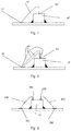
- the wafer circuit includes a wafer 10', an electrode 20', a bonding pad 30', and a bonding wire 40', wherein the electrode 20' is arranged on the wafer 10', and the electrode 20' is connected to the bonding pad 30'via the bonding wire 40'. Both the bonding pad 30' and the wafer 10'are arranged on a substrate. Thus, the whole wafer circuit will become abnormal once the bonding wire 40' is damaged.
- the major purpose of the present invention is to provide a wafer circuit so as to solve the problem in the related art that a wafer circuit is easy to become abnormal.
- a wafer circuit is provided according to the present invention so as to implement the purpose above.
- the wafer circuit includes: a wafer, fixed on a substrate; an electrode, arranged on the wafer; a bonding pad, arranged on the substrate; and a plurality of bonding wires with first ends all connected to the electrode and second ends all connected to the bonding pad, wherein the plurality of bonding wires are parallel bonding wires.
- the electrode is one electrode and the bonding pad is one bonding pad, and that the first ends of the plurality of bonding wires are all connected to the electrode and the second ends of the plurality of bonding wires are all connected to the bonding pad includes that the first ends of the plurality of bonding wires are all connected to the one electrode and the second ends of the plurality of bonding wires are all connected to the one bonding pad.
- the electrode is one electrode and the bonding pad is a plurality of bonding pads, and that the first ends of the plurality of bonding wires are all connected to the electrode and the second ends of the plurality of bonding wires are all connected to the bonding pad includes that the first ends of the plurality of bonding wires are all connected to the one electrode and the second ends of the plurality of bonding wires are connected to any bonding pad among the plurality of bonding pads.
- the electrode is one electrode and the bonding pad is a plurality of bonding pads, and that the first ends of the plurality of bonding wires are all connected to the electrode and the second ends of the plurality of bonding wires are all connected to the bonding pad includes that the first ends of the plurality of bonding wires are all connected to the one electrode and the second ends of the plurality of bonding wires are connected to different bonding pads among the plurality of bonding pads.
- the electrode includes a first electrode and a second electrode
- the bonding pad includes a first bonding pad and a second bonding pad
- the plurality of bonding wires include a first bonding wire and a second bonding wire
- the electrode is a plurality of electrodes
- the bonding pad is one bonding pad
- that the first ends of the plurality of bonding wires are all connected to the electrode and the second ends of the plurality of bonding wires are all connected to the bonding pad includes that the first ends of the plurality of bonding wires are connected to any electrode among the plurality of electrodes, and the second ends of the plurality of bonding wires are all connected to the one bonding pad.
- the electrode is a plurality of electrodes
- the bonding pad is one bonding pad
- that the first ends of the plurality of bonding wires are all connected to the electrode and the second ends of the plurality of bonding wires are all connected to the bonding pad includes that the first ends of the plurality of bonding wires are connected to different electrodes among the plurality of electrodes and the second ends of the plurality of bonding wires are all connected to the one bonding pad.
- the electrode is a plurality of electrodes
- the bonding pad is a plurality of bonding pads
- that the first ends of the plurality of bonding wires are all connected to the electrode and the second ends of the plurality of bonding wires are all connected to the bonding pad includes that the first ends of the plurality of bonding wires are connected to any electrode among the plurality of electrodes, and the second ends of the plurality of boding wires are connected to any bonding pad among the plurality of bonding pads.
- the electrode is a plurality of electrodes
- the bonding pad is a plurality of bonding pads
- that the first ends of the plurality of bonding wires are all connected to the electrode and the second ends of the plurality of bonding wires are all connected to the bonding pad includes that the first ends of the plurality of bonding wires are connected to different electrodes among the plurality of electrodes and the second ends of the plurality of bonding wires are connected to different bonding pads among the plurality of bonding pads.
- the electrode is a plurality of electrodes
- the bonding pad is a plurality of bonding pads
- that the first ends of the plurality of bonding wires are all connected to the electrode and the second ends of the plurality of bonding wires are all connected to the bonding pad includes that the first ends of the plurality of bonding wires are connected to any electrode among the plurality of electrodes and the second ends of the plurality of bonding wires are connected to different bonding pads among the plurality of bonding pads.
- the electrode is a plurality of electrodes
- the bonding pad is a plurality of bonding pads
- that the first ends of the plurality of bonding wires are all connected to the electrode and the second ends of the plurality of bonding wires are all connected to the bonding pad includes that the first ends of the plurality of bonding wires are connected to different electrodes among the plurality of electrodes and the second ends of the plurality of bonding wires are connected to any bonding pad among the plurality of bonding pads.
- the electrodes are arranged at a P type material side of the wafer simultaneously, or arranged at an N type material side of the wafer simultaneously.
- the present invention applies a wafer, fixed on a substrate; an electrode, arranged on the wafer; a bonding pad, arranged on the substrate; and a plurality of bonding wires with first ends all connected to the electrode and second ends all connected to the bonding pad, wherein the plurality of bonding wires are parallel bonding wires, thus the electrode and the bonding pad will not be disconnected even if a certain bonding wire or some bonding wires are damaged, thereby solving the problem in the related art that a wafer circuit is easy to become abnormal and further achieving the effect of reducing the probability that the wafer circuit becomes abnormal.
- a wafer circuit is provided according to an embodiment of the present invention.
- the wafer circuit is used for utilizing a plurality of bonding wires to reduce the probability that a wafer circuit becomes abnormal.
- Fig. 2 is a schematic diagram of a wafer circuit according to an embodiment of the present invention.
- the wafer circuit includes: a wafer 10, an electrode 20, a bonding pad 30, and a bonding wire 40, wherein the bonding wire 40 includes any number of bonding wires, and three bonding wires 40 are described in the present embodiment.
- the wafer 10 is fixed on a substrate, wherein the wafer 10 may be fixed on the substrate by glue.
- the glue may be silver glue or insulating cement and the substrate may be a Printed Circuit Board (PCB).
- the electrode 20 is arranged on the wafer 10.
- the electrode 20 may include one or more.
- the electrode may be arranged on a P type material side or an N type material side of the wafer 10.
- the plurality of electrodes 20 may be arranged on the P type material side of the wafer 10 simultaneously, or arranged on the N type material side of the wafer 10 simultaneously.
- the bonding pad 30 is arranged on the substrate, wherein there may be one or more bonding pads 30.
- the plurality of bonding wires 40 connected between the electrode 20 and the bonding pad 30 are necessarily parallel bonding wires.
- the plurality of bonding pads 30 may be connected via the bonding wires on the substrate, thus the plurality of bonding wires 40 between the plurality of bonding pads 30 and the electrode 20 are parallel bonding wires.
- First ends of the plurality of bonding wires 40 are all connected to the electrode 20, and second ends of the plurality of bonding wires 40 are all connected to the bonding pad 30, wherein the plurality of bonding wires 40 are parallel bonding wires.
- the three bonding wires are bonding wire 401, bonding wire 402 and bonding wire 403, respectively. First ends of the three bonding wires are all connected to the electrode 20 and second ends of the three bonding wires are all connected to the bonding pad 30.
- the electrode 20 may be only one kind of electrode 20 arranged on the wafer 10, i.e. a first electrode. If the electrode 20 is arranged at the P type material side of the wafer 10, the polarity of the electrode 20 is "+” and the electrode may be connected to the "+” pole on the substrate via the plurality of bonding wires 30, while the N type material side of the wafer 10 may be connected with the "-" pole on the substrate directly. In this way, a PN junction of the wafer 10 may be conducted after a power source is turned on, so as to recombine holes and electrons and release energy in the form of photons to enable an LED to emit lights.
- the electrode 20 is arranged at the N type material side of the wafer 10, the polarity of the electrode 20 is "-" and the electrode may be connected to the "-" pole on the substrate through the plurality of bonding wires 30, while the P type material side of the wafer 10 may be connected with the "+” pole on the substrate directly.
- a PN junction of the wafer 10 may be conducted when a power source is turned on so as to recombine holes and electrons and release energy in the form of photons to enable an LED to emit lights.
- a second electrode may be also arranged on the wafer 10 besides one electrode, i.e. the electrode 20 (the first electrode) in an embodiment of the present invention.
- the electrode 20 is arranged at the P type material side of the wafer 10
- the polarity of the electrode 20 is "+” and the electrode may be connected to the "+” pole on the substrate via the plurality of bonding wires 30, while the second electrode may be connected with the "-" pole on the substrate.
- a PN junction of the wafer 10 may be conducted after a power source is turned on, so as to recombine holes and electrons and release energy in the form of photons to enable an LED to emit lights.
- the electrode 20 is arranged at the N type material side of the wafer 10, the polarity of the electrode 20 is "-", and the electrode may be connected to the "-" pole on the substrate through the plurality of bonding wires 30, while the second electrode may be connected with the "+” pole on the substrate.
- a PN junction of the wafer 10 may be conducted when the power source is turned on so as to recombine holes and electrons and release energy in the form of photons to enable an LED to emit lights.
- a plurality of bonding wires 40 are connected between an electrode 20 and a bonding pad 3.
- a wafer circuit will not become abnormal as long as at least one bonding wire 40 is connected between the electrode 20 and the bonding pad 30 if some bonding wires 40 in one or more bonding wires 40 are damaged, thereby achieving the effect of reducing the probability that the wafer circuit becomes abnormal.
- Electrodes 20 and bonding pads 30 there may be one or more electrodes 20 and bonding pads 30 in the embodiments of the present invention. If there is a plurality of electrodes 20 and/or bonding pads 30, an abnormality of the wafer circuit, which is caused by damage of an electrode 20 and/or separation of a bonding pad 30, may be avoided.
- Multilayer protection may be provided for the wafer circuit by arranging a plurality of bonding wires 40 and/or a plurality of electrodes 20 and/or a plurality of bonding pads 30 in the wafer circuit, thereby preventing the wafer circuit from becoming abnormal due to reasons including damage of a bonding wire 40 and/or damage of an electrode and/or separation of a bonding pad 30, and so on, wherein combining methods and corresponding connection methods of an electrode 20 and a bonding pad 30 in the wafer circuit may be as follows in the case that there may be one or more electrodes 20 and bonding pads 30.
- the first ends of the plurality of bonding wires 40 may be all connected on the same electrode 20 and the second ends of the plurality of bonding wires 40 may be all connected on the same bonding pad 40, and after being connected in this way, the plurality of bonding wires 40 are necessarily parallel bonding wires. Since the electrode 20 and the bonding pad 30 are connected by the plurality of bonding wires 40, it may be ensured that the electrode 20 and the bonding pad 30 are connected as long as there is an undamaged bonding wire 40 between the electrode 20 and the bonding pad 30 regardless of a damaged bonding wire 40, thereby ensuring that the wafer circuit is normal.
- the first ends of the plurality of bonding wires 40 may be all connected on the same electrode 20 and the second ends of the plurality of bonding wires 40 may be all connected to any bonding pad 30 among the plurality of bonding pads 30. It needs to be noted that the plurality of bonding wires 40 connected on any bonding pad 30 are parallel bonding wires.
- the electrode 20 and the bonding pads 30 are connected by the plurality of bonding wires 40, it may be ensured that the electrode 20 and the bonding pads 30 are connected as long as there is an undamaged bonding wire 40 between the electrode 20 and the bonding pads 30 regardless of a damaged bonding wire 40, thereby ensuring that the wafer circuit is normal.
- the plurality of parallel bonding wires 40 may be connected on the plurality of bonding pads 30, the normality of the whole wafer circuit will not be affected even if a bonding pad 30 is separated.
- the first ends of the plurality of bonding wires 40 may be all connected on the same electrode 20 and the second ends of the plurality of bonding wires may be connected to different bonding pads 30 among the plurality of bonding pads 30. It needs to be noted that the plurality of bonding wires 40 connected on different bonding pads 30 are parallel bonding wires. Based on the same reason as that in the second method (which will not be described repeatedly here), the normality of the whole wafer circuit will not be affected even if a bonding pad 30 is separated.
- the bonding pad 30 includes a first bonding pad 301 and a second bonding pad 302
- the plurality of bonding wires 40 include a first bonding wire 404 and a second bonding wire 405, wherein the first electrode and the second electrode are arranged at the P type material side or the N type material side of the wafer 10 simultaneously, or the two are on different locations, and the first bonding pad and the second bonding pad are arranged on different locations of the substrate respectively, a first end of the first bonding wire may be connected to the first electrode, a second end of the first bonding wire may be connected to the first bonding pad, a first end of the second bonding wire may be connected to the second electrode and a second end of the second bonding wire may be connected to the second bonding pad.
- the first bonding wire and the second bonding wire are parallel bonding wires. Since the first bonding wire and the second bonding wire, which are parallel with each other, are connected between the first electrode and first bonding pad, and between the second electrode and the second bonding pad, respectively, the whole wafer circuit will not become abnormal as long as either or both of the first bonding wire and the second bonding wire are undamaged. In the meanwhile, since different bonding wires are connected to different electrodes and bonding pads, the whole wafer circuit will not become abnormal even if one electrode or one bonding pad is damaged, thus multilayer protection is provided for the wafer circuit by the electrodes 20, the bonding pads 30 and the bonding wires 40, as shown in Fig. 3 .
- the first ends of the plurality of bonding wires 40 may be connected to any electrode among the plurality of electrodes 20, and the second ends of the plurality of bonding wires 40 may be all connected to the same bonding pad 30, wherein the plurality of bonding wires 40 are parallel bonding wires. Since the electrodes 20 and the bonding pad 30 are connected by the plurality of bonding wires 40, it may be ensured that the electrodes 20 and the bonding pad 30 are connected as long as there is an undamaged bonding wire 40 between the electrodes 20 and the bonding pad 30 regardless of a damaged bonding wire 40, thereby ensuring that the wafer circuit is normal. In the meanwhile, since the plurality of parallel bonding wires 40 may be connected on the plurality of electrodes 20, the normality of the whole wafer circuit will not be affected even if an electrode 20 is damaged.
- the first ends of the plurality of bonding wires 40 may be connected to different electrodes among the plurality of electrodes 20 and the second ends of the plurality of bonding wires 40 may be connected on the same bonding pad 30, wherein the plurality of bonding wires 40 are parallel bonding wires. Based on the same reason as that in the fifth method (which will not be described repeatedly here), the normality of the whole wafer circuit will not be affected even if an electrode 20 is damaged.
- the first ends of the plurality of bonding wires 40 may be connected to any electrode among the plurality of electrodes 20, and the second ends of the plurality of boding wires may be connected to any bonding pad among the plurality of bonding pads 30, wherein the plurality of bonding wires 40 are parallel bonding wires.
- the normality of the whole wafer circuit will not be affected even if an electrode 20 is damaged, or a bonding pad 30 is separated or a bonding wire 40 is damaged.
- the first ends of the plurality of bonding wires 40 are connected to different electrodes among the plurality of electrodes 20 and the second ends of the plurality of bonding wires 40 are connected to different bonding pads among the plurality of bonding pads 30, wherein the plurality of bonding wires 40 are parallel bonding wires.
- the normality of the whole wafer circuit will not be affected even if an electrode 20 is damaged, or a bonding pad 30 is separated or a bonding wire 40 is damaged.
- the first ends of the plurality of bonding wires 40 may be connected to any electrode among the plurality of electrodes 20 and the second ends of the plurality of bonding wires 40 may be connected to different bonding pads among the plurality of bonding pads 30.
- the normality of the whole wafer circuit will not be affected even if an electrode 20 is damaged, or a bonding pad 30 is separated or a bonding wire 40 is damaged.
- the first ends of the plurality of bonding wires 40 may be connected to different electrodes among the plurality of electrodes 20 and the second ends of the plurality of bonding wires 40 may be connected to any bonding pad among the plurality of bonding pads 30.
- the normality of the whole wafer circuit will not be affected even if an electrode 20 is damaged, or a bonding pad 30 is separated or a bonding wire 40 is damaged.
- the electrode 20 when the electrode 20 is a plurality of electrodes 20, the plurality of electrodes 20 may be arranged at a P type material side of the wafer 10 simultaneously, or arranged at an N type material side of the wafer 10 simultaneously.
Landscapes
- Wire Bonding (AREA)
- Led Device Packages (AREA)
- Physics & Mathematics (AREA)
- Geometry (AREA)
- Semiconductor Integrated Circuits (AREA)
Applications Claiming Priority (2)
| Application Number | Priority Date | Filing Date | Title |
|---|---|---|---|
| CN201410137106.6A CN103904207A (zh) | 2014-04-04 | 2014-04-04 | 晶片电路 |
| PCT/CN2014/084027 WO2015149462A1 (fr) | 2014-04-04 | 2014-08-08 | Circuit sur plaquette |
Publications (2)
| Publication Number | Publication Date |
|---|---|
| EP3128552A1 true EP3128552A1 (fr) | 2017-02-08 |
| EP3128552A4 EP3128552A4 (fr) | 2018-02-28 |
Family
ID=50995440
Family Applications (1)
| Application Number | Title | Priority Date | Filing Date |
|---|---|---|---|
| EP14887860.6A Withdrawn EP3128552A4 (fr) | 2014-04-04 | 2014-08-08 | Circuit sur plaquette |
Country Status (7)
| Country | Link |
|---|---|
| US (1) | US20170025376A1 (fr) |
| EP (1) | EP3128552A4 (fr) |
| JP (1) | JP6317454B2 (fr) |
| KR (1) | KR20160142276A (fr) |
| CN (1) | CN103904207A (fr) |
| CA (1) | CA2936655A1 (fr) |
| WO (1) | WO2015149462A1 (fr) |
Families Citing this family (3)
| Publication number | Priority date | Publication date | Assignee | Title |
|---|---|---|---|---|
| CN103904207A (zh) * | 2014-04-04 | 2014-07-02 | 利亚德光电股份有限公司 | 晶片电路 |
| CN106683574A (zh) * | 2015-11-11 | 2017-05-17 | 利亚德光电股份有限公司 | 发光二极管显示屏及其用途 |
| DE102024102633A1 (de) * | 2024-01-30 | 2025-07-31 | Ams-Osram International Gmbh | Optoelektronisches halbleiterbauelement |
Family Cites Families (33)
| Publication number | Priority date | Publication date | Assignee | Title |
|---|---|---|---|---|
| JPS6184077A (ja) * | 1984-10-01 | 1986-04-28 | Toshiba Corp | 発光素子アレイ |
| GB8711373D0 (en) * | 1987-05-14 | 1987-06-17 | Secr Defence | Electroluminescent silicon device |
| US5399903A (en) * | 1990-08-15 | 1995-03-21 | Lsi Logic Corporation | Semiconductor device having an universal die size inner lead layout |
| JP3618989B2 (ja) * | 1997-12-24 | 2005-02-09 | 株式会社東芝 | 半導体レーザ装置 |
| US6476506B1 (en) * | 2001-09-28 | 2002-11-05 | Motorola, Inc. | Packaged semiconductor with multiple rows of bond pads and method therefor |
| CN2612075Y (zh) * | 2003-02-08 | 2004-04-14 | 光鼎电子股份有限公司 | Led封装结构 |
| US20060087013A1 (en) * | 2004-10-21 | 2006-04-27 | Etron Technology, Inc. | Stacked multiple integrated circuit die package assembly |
| JP4815843B2 (ja) * | 2005-04-01 | 2011-11-16 | 日亜化学工業株式会社 | 発光装置 |
| JP5237539B2 (ja) * | 2005-09-20 | 2013-07-17 | パナソニック株式会社 | 発光装置 |
| US7598599B2 (en) * | 2006-03-09 | 2009-10-06 | Stats Chippac Ltd. | Semiconductor package system with substrate having different bondable heights at lead finger tips |
| TWI320593B (en) * | 2006-04-10 | 2010-02-11 | Advanced Semiconductor Eng | Common assembly substrate and applying mechanisms thereof |
| CN100511664C (zh) * | 2006-07-11 | 2009-07-08 | 日月光半导体制造股份有限公司 | 芯片封装结构 |
| JP5023781B2 (ja) * | 2006-11-13 | 2012-09-12 | 日亜化学工業株式会社 | 発光装置 |
| JP5084015B2 (ja) * | 2007-05-15 | 2012-11-28 | シチズン電子株式会社 | 発光ダイオードの製造方法 |
| JP5082710B2 (ja) * | 2007-09-19 | 2012-11-28 | 日亜化学工業株式会社 | 発光装置 |
| JP5595694B2 (ja) * | 2009-01-15 | 2014-09-24 | パナソニック株式会社 | 半導体装置 |
| US9627361B2 (en) * | 2010-10-07 | 2017-04-18 | Cree, Inc. | Multiple configuration light emitting devices and methods |
| KR101707118B1 (ko) * | 2010-10-19 | 2017-02-15 | 엘지이노텍 주식회사 | 발광소자 및 그 발광 소자의 제조 방법 |
| CN102456825A (zh) * | 2010-10-25 | 2012-05-16 | 展晶科技(深圳)有限公司 | 发光二极管及其制造方法 |
| US9123713B2 (en) * | 2010-11-24 | 2015-09-01 | Tessera, Inc. | Lead structures with vertical offsets |
| JP3167669U (ja) * | 2011-02-21 | 2011-05-12 | 鼎元光電科技股▲ふん▼有限公司 | ハイパワー垂直型発光ダイオード |
| US20120228759A1 (en) * | 2011-03-07 | 2012-09-13 | Wen-Jeng Fan | Semiconductor package having interconnection of dual parallel wires |
| US8901578B2 (en) * | 2011-05-10 | 2014-12-02 | Rohm Co., Ltd. | LED module having LED chips as light source |
| CN202150488U (zh) * | 2011-07-17 | 2012-02-22 | 吴发模 | 一种用于led晶片的贴装结构 |
| KR20130104430A (ko) * | 2012-03-14 | 2013-09-25 | 삼성전자주식회사 | 멀티-칩 패키지 및 그의 제조 방법 |
| TWI528510B (zh) * | 2012-03-19 | 2016-04-01 | 鴻海精密工業股份有限公司 | 晶片組裝結構及晶片組裝方法 |
| US9515055B2 (en) * | 2012-05-14 | 2016-12-06 | Cree, Inc. | Light emitting devices including multiple anodes and cathodes |
| JP2014011396A (ja) * | 2012-07-02 | 2014-01-20 | Aoi Electronics Co Ltd | 半導体装置の実装構造および半導体装置の実装方法 |
| DE102012109107A1 (de) * | 2012-09-26 | 2014-03-27 | Osram Opto Semiconductors Gmbh | Schaltungsanordnung |
| CN202977406U (zh) * | 2012-11-14 | 2013-06-05 | 华东科技股份有限公司 | 避免打线造成晶片断裂的多晶片堆叠封装结构 |
| CN103606609B (zh) * | 2013-10-21 | 2016-08-17 | 溧阳市东大技术转移中心有限公司 | 一种发光二极管电极的制造方法 |
| CN103904207A (zh) * | 2014-04-04 | 2014-07-02 | 利亚德光电股份有限公司 | 晶片电路 |
| CN203871371U (zh) * | 2014-04-04 | 2014-10-08 | 利亚德光电股份有限公司 | 晶片电路 |
-
2014
- 2014-04-04 CN CN201410137106.6A patent/CN103904207A/zh active Pending
- 2014-08-08 CA CA2936655A patent/CA2936655A1/fr not_active Abandoned
- 2014-08-08 JP JP2016543228A patent/JP6317454B2/ja active Active
- 2014-08-08 KR KR1020167017046A patent/KR20160142276A/ko not_active Ceased
- 2014-08-08 WO PCT/CN2014/084027 patent/WO2015149462A1/fr not_active Ceased
- 2014-08-08 EP EP14887860.6A patent/EP3128552A4/fr not_active Withdrawn
- 2014-08-08 US US15/111,774 patent/US20170025376A1/en not_active Abandoned
Also Published As
| Publication number | Publication date |
|---|---|
| US20170025376A1 (en) | 2017-01-26 |
| KR20160142276A (ko) | 2016-12-12 |
| CA2936655A1 (fr) | 2015-10-08 |
| EP3128552A4 (fr) | 2018-02-28 |
| CN103904207A (zh) | 2014-07-02 |
| WO2015149462A1 (fr) | 2015-10-08 |
| JP6317454B2 (ja) | 2018-04-25 |
| JP2017511598A (ja) | 2017-04-20 |
Similar Documents
| Publication | Publication Date | Title |
|---|---|---|
| JP2015012292A5 (fr) | ||
| JP2015076612A5 (fr) | ||
| CA2656198A1 (fr) | Fil lumineux a diodes electroluminescentes monopiece forme d'un seul tenant | |
| US11677057B2 (en) | Light emitting device, light emitting module, and illuminating apparatus | |
| EP2669962A3 (fr) | Dispositif électroluminescent semi-conducteur et son procédé de fabrication | |
| JP6256699B2 (ja) | 発光装置 | |
| US20170025376A1 (en) | Wafer circuit | |
| CN103292201A (zh) | 发光二极管灯条及应用其灯条的发光二极管模块 | |
| TW201042784A (en) | LED package structure | |
| EP3318109B1 (fr) | Dispositif d'éclairage à del | |
| JP6576094B2 (ja) | Led発光装置 | |
| US9484330B2 (en) | Light-emitting device | |
| CN203774366U (zh) | 一种立体发光led芯片灯丝及led灯泡 | |
| JP2014192313A5 (ja) | Led発光装置の製造方法及びled発光装置 | |
| TWI564505B (zh) | 燈條結構 | |
| CN203871371U (zh) | 晶片电路 | |
| KR20150077208A (ko) | 반도체 소자 패키지, 이를 포함하는 발광 다이오드 패키지 및 광학 모듈 | |
| JP2016031951A (ja) | Led発光モジュール | |
| CN202150488U (zh) | 一种用于led晶片的贴装结构 | |
| US20160013166A1 (en) | Light emitting module | |
| TWI636590B (zh) | 發光二極體封裝 | |
| CN202404841U (zh) | 2rgb全彩led显示屏 | |
| JP2012134306A (ja) | 発光装置及びそれを用いた照明装置 | |
| US20150159815A1 (en) | Direct-type illumination device and light bar structure for use therein | |
| CN103982803A (zh) | 一种新型多功能侧插式led模块及其实现方法 |
Legal Events
| Date | Code | Title | Description |
|---|---|---|---|
| PUAI | Public reference made under article 153(3) epc to a published international application that has entered the european phase |
Free format text: ORIGINAL CODE: 0009012 |
|
| STAA | Information on the status of an ep patent application or granted ep patent |
Free format text: STATUS: REQUEST FOR EXAMINATION WAS MADE |
|
| 17P | Request for examination filed |
Effective date: 20160708 |
|
| AK | Designated contracting states |
Kind code of ref document: A1 Designated state(s): AL AT BE BG CH CY CZ DE DK EE ES FI FR GB GR HR HU IE IS IT LI LT LU LV MC MK MT NL NO PL PT RO RS SE SI SK SM TR |
|
| AX | Request for extension of the european patent |
Extension state: BA ME |
|
| DAX | Request for extension of the european patent (deleted) | ||
| RIC1 | Information provided on ipc code assigned before grant |
Ipc: H01L 33/62 20100101ALI20171023BHEP Ipc: H01L 23/49 20060101AFI20171023BHEP |
|
| A4 | Supplementary search report drawn up and despatched |
Effective date: 20180130 |
|
| RIC1 | Information provided on ipc code assigned before grant |
Ipc: H01L 23/49 20060101AFI20180124BHEP Ipc: H01L 33/62 20100101ALI20180124BHEP |
|
| STAA | Information on the status of an ep patent application or granted ep patent |
Free format text: STATUS: EXAMINATION IS IN PROGRESS |
|
| 17Q | First examination report despatched |
Effective date: 20210628 |
|
| STAA | Information on the status of an ep patent application or granted ep patent |
Free format text: STATUS: THE APPLICATION IS DEEMED TO BE WITHDRAWN |
|
| 18D | Application deemed to be withdrawn |
Effective date: 20211109 |